FreshRSS

Zobrazení pro čtení

Jsou dostupné nové články, klikněte pro obnovení stránky.

Researchers harness 2D magnetic materials for energy-efficient computing

Experimental computer memories and processors built from magnetic materials use far less energy than traditional silicon-based devices. Two-dimensional magnetic materials, composed of layers that are only a few atoms thick, have incredible properties that could allow magnetic-based devices to achieve unprecedented speed, efficiency, and scalability.

While many hurdles must be overcome until these so-called van der Waals magnetic materials can be integrated into functioning computers, MIT researchers took an important step in this direction by demonstrating precise control of a van der Waals magnet at room temperature.

This is key, since magnets composed of atomically thin van der Waals materials can typically only be controlled at extremely cold temperatures, making them difficult to deploy outside a laboratory.

The researchers used pulses of electrical current to switch the direction of the device’s magnetization at room temperature. Magnetic switching can be used in computation, the same way a transistor switches between open and closed to represent 0s and 1s in binary code, or in computer memory, where switching enables data storage.

The team fired bursts of electrons at a magnet made of a new material that can sustain its magnetism at higher temperatures. The experiment leveraged a fundamental property of electrons known as spin, which makes the electrons behave like tiny magnets. By manipulating the spin of electrons that strike the device, the researchers can switch its magnetization.

“The heterostructure device we have developed requires an order of magnitude lower electrical current to switch the van der Waals magnet, compared to that required for bulk magnetic devices,” says Deblina Sarkar, the AT&T Career Development Assistant Professor in the MIT Media Lab and Center for Neurobiological Engineering, head of the Nano-Cybernetic Biotrek Lab, and the senior author of a paper on this technique. “Our device is also more energy efficient than other van der Waals magnets that are unable to switch at room temperature.”

In the future, such a magnet could be used to build faster computers that consume less electricity. It could also enable magnetic computer memories that are nonvolatile, which means they don’t leak information when powered off, or processors that make complex AI algorithms more energy-efficient.

“There is a lot of inertia around trying to improve materials that worked well in the past. But we have shown that if you make radical changes, starting by rethinking the materials you are using, you can potentially get much better solutions,” says Shivam Kajale, a graduate student in Sarkar’s lab and co-lead author of the paper.

Kajale and Sarkar are joined on the paper by co-lead author Thanh Nguyen, a graduate student in the Department of Nuclear Science and Engineering (NSE); Corson Chao, a graduate student in the Department of Materials Science and Engineering (DSME); David Bono, a DSME research scientist; Artittaya Boonkird, an NSE graduate student; and Mingda Li, associate professor of nuclear science and engineering. The research appears this week in Nature Communications.

An atomically thin advantage

Methods to fabricate tiny computer chips in a clean room from bulk materials like silicon can hamper devices. For instance, the layers of material may be barely 1 nanometer thick, so minuscule rough spots on the surface can be severe enough to degrade performance.

By contrast, van der Waals magnetic materials are intrinsically layered and structured in such a way that the surface remains perfectly smooth, even as researchers peel off layers to make thinner devices. In addition, atoms in one layer won’t leak into other layers, enabling the materials to retain their unique properties when stacked in devices.

“In terms of scaling and making these magnetic devices competitive for commercial applications, van der Waals materials are the way to go,” Kajale says.

But there’s a catch. This new class of magnetic materials have typically only been operated at temperatures below 60 kelvins (-351 degrees Fahrenheit). To build a magnetic computer processor or memory, researchers need to use electrical current to operate the magnet at room temperature.

To achieve this, the team focused on an emerging material called iron gallium telluride. This atomically thin material has all the properties needed for effective room temperature magnetism and doesn’t contain rare earth elements, which are undesirable because extracting them is especially destructive to the environment.

Nguyen carefully grew bulk crystals of this 2D material using a special technique. Then, Kajale fabricated a two-layer magnetic device using nanoscale flakes of iron gallium telluride underneath a six-nanometer layer of platinum.

Tiny device in hand, they used an intrinsic property of electrons known as spin to switch its magnetization at room temperature.

Electron ping-pong

While electrons don’t technically “spin” like a top, they do possess the same kind of angular momentum. That spin has a direction, either up or down. The researchers can leverage a property known as spin-orbit coupling to control the spins of electrons they fire at the magnet.

The same way momentum is transferred when one ball hits another, electrons will transfer their “spin momentum” to the 2D magnetic material when they strike it. Depending on the direction of their spins, that momentum transfer can reverse the magnetization.

In a sense, this transfer rotates the magnetization from up to down (or vice-versa), so it is called a “torque,” as in spin-orbit torque switching. Applying a negative electric pulse causes the magnetization to go downward, while a positive pulse causes it to go upward.

The researchers can do this switching at room temperature for two reasons: the special properties of iron gallium telluride and the fact that their technique uses small amounts of electrical current. Pumping too much current into the device would cause it to overheat and demagnetize.

The team faced many challenges over the two years it took to achieve this milestone, Kajale says. Finding the right magnetic material was only half the battle. Since iron gallium telluride oxidizes quickly, fabrication must be done inside a glovebox filled with nitrogen.

“The device is only exposed to air for 10 or 15 seconds, but even after that I have to do a step where I polish it to remove any oxide,” he says.

Now that they have demonstrated room-temperature switching and greater energy efficiency, the researchers plan to keep pushing the performance of magnetic van der Waals materials.

“Our next milestone is to achieve switching without the need for any external magnetic fields. Our aim is to enhance our technology and scale up to bring the versatility of van der Waals magnet to commercial applications,” Sarkar says.

This work was carried out, in part, using the facilities at MIT.Nano and the Harvard University Center for Nanoscale Systems.
© Image: Courtesy of the researchers

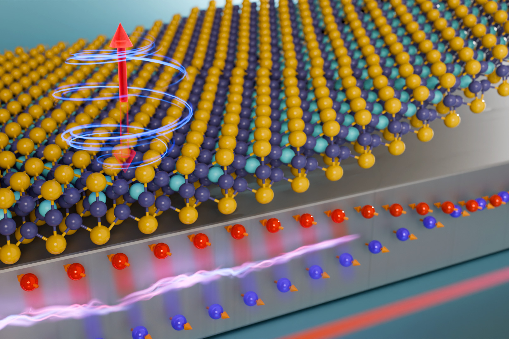
This illustration shows electric current being pumped into platinum (the bottom slab), which results in the creation of an electron spin current that switches the magnetic state of the 2D ferromagnet on top. The colored spheres represent the atoms in the 2D material.

Play it again, Spirio

Seated at the grand piano in MIT’s Killian Hall last fall, first-year student Jacqueline Wang played through the lively opening of Mozart’s “Sonata in B-flat major, K.333.” When she’d finished, Mi-Eun Kim, pianist and lecturer in MIT’s Music and Theater Arts Section (MTA), asked her to move to the rear of the hall. Kim tapped at an iPad. Suddenly, the sonata she'd just played poured forth again from the piano — its keys dipping and rising just as they had with Wang’s fingers on them, the resonance of its strings filling the room. Wang stood among a row of empty seats with a slightly bemused expression, taking in a repeat of her own performance.

“That was a little strange,” Wang admitted when the playback concluded, then added thoughtfully: “It sounds different from what I imagine I’m playing.”

This unusual lesson took place during a nearly three-week residency at MIT of the Steinway Spirio | r, a piano embedded with technology for live performance capture and playback. “The residency offered students, faculty, staff, and campus visitors the opportunity to engage with this new technology through a series of workshops that focused on such topics as the historical analysis of piano design, an examination of the hardware and software used by the Spirio | r, and step-by-step guidance of how to use the features,” explains Keeril Makan, head of MIT Music and Theater Arts and associate dean of the School of Humanities, Arts, and Social Sciences.

Wang was one of several residency participants to have the out-of-body experience of hearing herself play from a different vantage point, while watching the data of her performance scroll across a screen: color-coded rectangles indicating the velocity and duration of each note, an undulating line charting her use of the damper pedal. Wang was even able to edit her own performance, as she discovered when Kim suggested her rhythmic use of the pedal might be superfluous. Using the iPad interface to erase the pedaling entirely, they listened to the playback again, the notes gaining new clarity.

“See? We don’t need it,” Kim confirmed with a smile.

“When MIT’s new music building (W18) opens in spring 2025, we hope it will include this type of advanced technology. It would add value not just to Wang’s cohort of 19 piano students in the Emerson/Harris Program, which provides a total of 71 scholars and fellows with support for conservatory-level instruction in classical, jazz, and world music. But could also offer educational opportunities to a much wider swath of the MIT community,” says Makan. “Music is the fifth-most popular minor at MIT; 1,700 students enroll in music and theater arts classes each semester, and the Institute is brimming with vocalists, composers, instrumentalists, and music history students.”

According to Kim, the Spirio enables insights beyond what musicians could learn from a conventional recording; hearing playback directly from the instrument reveals sonic dimensions an MP3 can’t capture. “Speaker systems sort of crunch everything down — the highs and the lows, they all kind of sound the same. But piano solo music is very dynamic. It’s supposed to be experienced in a room,” she says.

During the Spirio | r residency, students found they could review their playing at half speed, adjust the volume of certain notes to emphasize a melody, transpose a piece to another key, or layer their performance — prerecording one hand, for example, then accompanying it live with the other.

“It helps the student be part of the learning and the teaching process,” Kim says. “If there’s a gap between what they imagined and what they hear and then they come to me and say, ‘How do I fix this?’ they’re definitely more engaged. It’s an honest representation of their playing, and the students who are humbled by it will become better pianists.”

For Wang, reflecting on her lesson with Kim, the session introduced an element she’d never experienced since beginning her piano studies at age 5. “The visual display of how long each key was played and with what velocity gave me a more precise demonstration of the ideas of voicing and evenness,” Wang says. “Playing the piano is usually dependent solely on the ears, but this combines with the auditory experience a visual experience and statistics, which helped me get a more holistic view of my playing.”

As a first-year undergraduate considering a Course 6 major (electrical engineering and computer science, or EECS), Wang was also fascinated to watch Patrick Elisha, a representative from Steinway dealer M. Steinert & Sons, disassemble the piano action to point out the optical sensors that measure the velocity of each hammer strike at 1,020 levels of sensitivity, sampled 800 times per second.

“I was amazed by the precision of the laser sensors and inductors,” says Wang. “I have just begun to take introductory-level courses in EECS and am just coming across these concepts, and this certainly made me more excited to learn more about these electrical devices and their applications. I was also intrigued that the electrical system was added onto the piano without interfering with the mechanical structure, so that when we play the Spirio, our experience with the touch and finger control was just like that of playing a usual Steinway.”

Another Emerson/Harris scholar, Víctor Quintas-Martínez, a PhD candidate in economics who resumed his lapsed piano studies during the Covid-19 pandemic, visited Killian Hall during the residency to rehearse a Fauré piano quartet with a cellist, violist, and violinist. “We did a run of certain passages and recorded the piano part. Then I listened to the strings play with the recording from the back of the hall. That gave me an idea of what I needed to adjust in terms of volume, texture, pedal, etc., to achieve a better balance. Normally, when you’re playing, because you’re sitting behind the strings and close to the piano, your perception of balance may be somewhat distorted,” he notes.

Kim cites another campus demographic ripe for exploring these types of instruments like the Spirio | r and its software: future participants in MIT’s relatively new Music Technology Master's Program, along with others across the Institute whose work intersects with the wealth of data the instrument captures. Among them is Praneeth Namburi, a research scientist at the MIT.nano Immersion Lab. Typically, Namburi focuses his neuroscience expertise on the biomechanics of dancing and expert movement. For two days during the MTA/Spirio residency, he used the sensors at the Immersion Lab, along with those of the Spirio, to analyze how pianists use their bodies.

“We used motion capture that can help us contrast the motion paths of experts such as Mi-Eun from those of students, potentially aiding in music education,” Namburi recounts, “force plates that can give scientific insights into how movement timing is organized, and ultrasound to visualize the forearm tissues during playing, which can potentially help us understand musicianship-related injuries.”

“The encounter between MTA and MIT.nano was something unique to MIT,” Kim believes. “Not only is this super useful for the music world, but it’s also very exciting for movement researchers, because playing piano is one of the most complex activities that humans do with our hands.”

In Kim’s view, that quintessentially human complexity is complemented by these kinds of technical possibilities. “Some people might think oh, it's going to replace the pianist,” she says. “But in the end it is a tool. It doesn’t replace all of the things that go into learning music. I think it's going to be an invaluable third partner: the student, the teacher, and the Spirio — or the musician, the researcher, and the Spirio. It's going to play an integral role in a lot of musical endeavors.”

© Still from a video by Trillium Studios/Arts at MIT; videography by Seven Generations

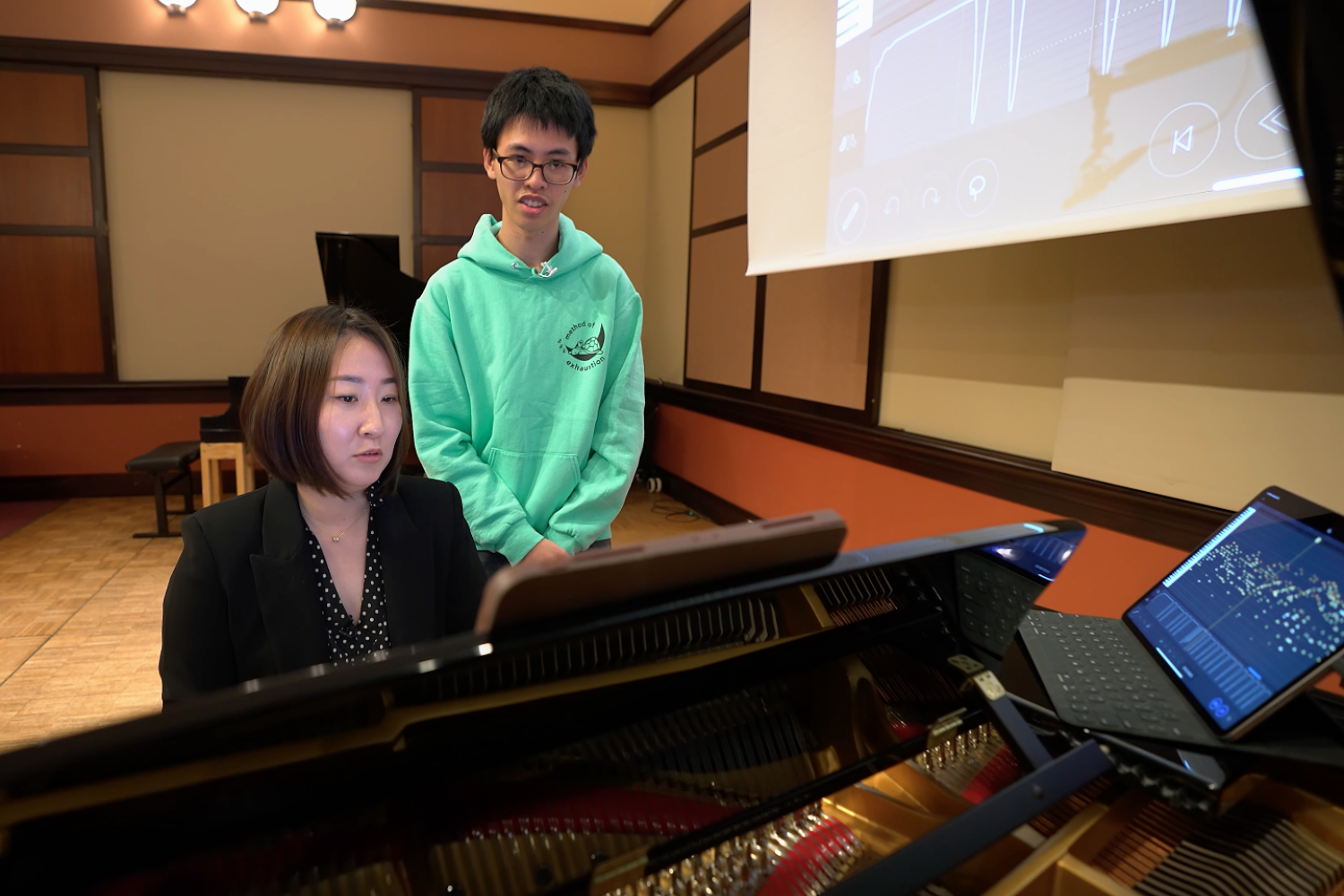
Mi-Eun Kim (seated), pianist and lecturer at MIT Music and Theater Arts, and student Holden Mui interact with the Steinway Spirio.

Technique could improve the sensitivity of quantum sensing devices

In quantum sensing, atomic-scale quantum systems are used to measure electromagnetic fields, as well as properties like rotation, acceleration, and distance, far more precisely than classical sensors can. The technology could enable devices that image the brain with unprecedented detail, for example, or air traffic control systems with precise positioning accuracy.

As many real-world quantum sensing devices are emerging, one promising direction is the use of microscopic defects inside diamonds to create “qubits” that can be used for quantum sensing. Qubits are the building blocks of quantum devices.

Researchers at MIT and elsewhere have developed a technique that enables them to identify and control a greater number of these microscopic defects. This could help them build a larger system of qubits that can perform quantum sensing with greater sensitivity.

Their method builds off a central defect inside a diamond, known as a nitrogen-vacancy (NV) center, which scientists can detect and excite using laser light and then control with microwave pulses. This new approach uses a specific protocol of microwave pulses to identify and extend that control to additional defects that can’t be seen with a laser, which are called dark spins.

The researchers seek to control larger numbers of dark spins by locating them through a network of connected spins. Starting from this central NV spin, the researchers build this chain by coupling the NV spin to a nearby dark spin, and then use this dark spin as a probe to find and control a more distant spin which can’t be sensed by the NV directly. The process can be repeated on these more distant spins to control longer chains.

“One lesson I learned from this work is that searching in the dark may be quite discouraging when you don’t see results, but we were able to take this risk. It is possible, with some courage, to search in places that people haven’t looked before and find potentially more advantageous qubits,” says Alex Ungar, a PhD student in electrical engineering and computer science and a member of the Quantum Engineering Group at MIT, who is lead author of a paper on this technique, which is published today in PRX Quantum.

His co-authors include his advisor and corresponding author, Paola Cappellaro, the Ford Professor of Engineering in the Department of Nuclear Science and Engineering and professor of physics; as well as Alexandre Cooper, a senior research scientist at the University of Waterloo’s Institute for Quantum Computing; and Won Kyu Calvin Sun, a former researcher in Cappellaro’s group who is now a postdoc at the University of Illinois at Urbana-Champaign.

Diamond defects

To create NV centers, scientists implant nitrogen into a sample of diamond.

But introducing nitrogen into the diamond creates other types of atomic defects in the surrounding environment. Some of these defects, including the NV center, can host what are known as electronic spins, which originate from the valence electrons around the site of the defect. Valence electrons are those in the outermost shell of an atom. A defect’s interaction with an external magnetic field can be used to form a qubit.

Researchers can harness these electronic spins from neighboring defects to create more qubits around a single NV center. This larger collection of qubits is known as a quantum register. Having a larger quantum register boosts the performance of a quantum sensor.

Some of these electronic spin defects are connected to the NV center through magnetic interaction. In past work, researchers used this interaction to identify and control nearby spins. However, this approach is limited because the NV center is only stable for a short amount of time, a principle called coherence. It can only be used to control the few spins that can be reached within this coherence limit.

In this new paper, the researchers use an electronic spin defect that is near the NV center as a probe to find and control an additional spin, creating a chain of three qubits.

They use a technique known as spin echo double resonance (SEDOR), which involves a series of microwave pulses that decouple an NV center from all electronic spins that are interacting with it. Then, they selectively apply another microwave pulse to pair the NV center with one nearby spin.

Unlike the NV, these neighboring dark spins can’t be excited, or polarized, with laser light. This polarization is a required step to control them with microwaves.

Once the researchers find and characterize a first-layer spin, they can transfer the NV’s polarization to this first-layer spin through the magnetic interaction by applying microwaves to both spins simultaneously. Then once the first-layer spin is polarized, they repeat the SEDOR process on the first-layer spin, using it as a probe to identify a second-layer spin that is interacting with it.

Controlling a chain of dark spins

This repeated SEDOR process allows the researchers to detect and characterize a new, distinct defect located outside the coherence limit of the NV center. To control this more distant spin, they carefully apply a specific series of microwave pulses that enable them to transfer the polarization from the NV center along the chain to this second-layer spin.

“This is setting the stage for building larger quantum registers to higher-layer spins or longer spin chains, and also showing that we can find these new defects that weren’t discovered before by scaling up this technique,” Ungar says.

To control a spin, the microwave pulses must be very close to the resonance frequency of that spin. Tiny drifts in the experimental setup, due to temperature or vibrations, can throw off the microwave pulses.

The researchers were able to optimize their protocol for sending precise microwave pulses, which enabled them to effectively identify and control second-layer spins, Ungar says.

“We are searching for something in the unknown, but at the same time, the environment might not be stable, so you don’t know if what you are finding is just noise. Once you start seeing promising things, you can put all your best effort in that one direction. But before you arrive there, it is a leap of faith,” Cappellaro says.

While they were able to effectively demonstrate a three-spin chain, the researchers estimate they could scale their method to a fifth layer using their current protocol, which could provide access to hundreds of potential qubits. With further optimization, they may be able to scale up to more than 10 layers.

In the future, they plan to continue enhancing their technique to efficiently characterize and probe other electronic spins in the environment and explore different types of defects that could be used to form qubits.

This research is supported, in part, by the U.S. National Science Foundation and the Canada First Research Excellence Fund.

© Image: Courtesy of the researchers

Researchers use microscopic defects inside a diamond to build a chain of three qubits (pictured as small circles with arrows) that they can use for quantum sensing. They start from a central defect, couple it with a nearby defect, and then use this second defect to find and control a third defect.

MIT-led team receives funding to pursue new treatments for metabolic disease

A team of MIT researchers will lead a $65.67 million effort, awarded by the U.S. Advanced Research Projects Agency for Health (ARPA-H), to develop ingestible devices that may one day be used to treat diabetes, obesity, and other conditions through oral delivery of mRNA. Such devices could potentially be deployed for needle-free delivery of mRNA vaccines as well.

The five-year project also aims to develop electroceuticals, a new form of ingestible therapies based on electrical stimulation of the body’s own hormones and neural signaling. If successful, this approach could lead to new treatments for a variety of metabolic disorders.

“We know that the oral route is generally the preferred route of administration for both patients and health care providers,” says Giovanni Traverso, an associate professor of mechanical engineering at MIT and a gastroenterologist at Brigham and Women’s Hospital. “Our primary focus is on disorders of metabolism because they affect a lot of people, but the platforms we’re developing could be applied very broadly.”

Traverso is the principal investigator for the project, which also includes Robert Langer, MIT Institute Professor, and Anantha Chandrakasan, dean of the MIT School of Engineering and the Vannevar Bush Professor of Electrical Engineering and Computer Science. As part of the project, the MIT team will collaborate with investigators from Brigham and Women’s Hospital, New York University, and the University of Colorado School of Medicine.

Over the past several years, Traverso’s and Langer’s labs have designed many types of ingestible devices that can deliver drugs to the GI tract. This approach could be especially useful for protein drugs and nucleic acids, which typically can’t be given orally because they break down in the acidic environment of the digestive tract.

Messenger RNA has already proven useful as a vaccine, directing cells to produce fragments of viral proteins that trigger an immune response. Delivering mRNA to cells also holds potential to stimulate production of therapeutic molecules to treat a variety of diseases. In this project, the researchers plan to focus on metabolic diseases such as diabetes.

“What mRNA can do is enable the potential for dosing therapies that are very difficult to dose today, or provide longer-term coverage by essentially creating an internal factory that produces a therapy for a prolonged period,” Traverso says.

In the mRNA portion of the project, the research team intends to identify lipid and polymer nanoparticle formulations that can most effectively deliver mRNA to cells, using machine learning to help identify the best candidates. They will also develop and test ingestible devices to carry the mRNA-nanoparticle payload, with the goal of running a clinical trial in the final year of the five-year project.

The work will build on research that Traverso’s lab has already begun. In 2022, Traverso and his colleagues reported that they could deliver mRNA in capsules that inject mRNA-nanoparticle complexes into the lining of the stomach.

The other branch of the project will focus on ingestible devices that can deliver a small electrical current to the lining of the stomach. In a study published last year, Traverso’s lab demonstrated this approach for the first time, using a capsule coated with electrodes that apply an electrical current to cells of the stomach. In animal studies, they found that this stimulation boosted production of ghrelin, a hormone that stimulates appetite.

Traverso envisions that this type of treatment could potentially replace or complement some of the existing drugs used to prevent nausea and stimulate appetite in people with anorexia or cachexia (loss of body mass that can occur in patients with cancer or other chronic diseases). The researchers also hope to develop ways to stimulate production of GLP-1, a hormone that is used to help manage diabetes and promote weight loss.

“What this approach starts to do is potentially maximize our ability to treat disease without administering a new drug, but instead by simply modulating the body’s own systems through electrical stimulation,” Traverso says.

At MIT, Langer will help to develop nanoparticles for mRNA delivery, and Chandrakasan will work on ways to reduce energy consumption and miniaturize the electronic functions of the capsules, including secure communication, stimulation, and power generation.

The Brigham and Women’s Hospital’s portion of the project will be co-led by Traverso, Ameya Kirtane, Jason Li, and Peter Chai, who will amplify efforts on the formulation and stabilization of the mRNA nanoparticles, engineering of the ingestible devices, and running of clinical trials. At NYU, the effort will be led by assistant professor of bioengineering Khalil Ramadi SM ’16, PhD ’19, focusing on biological characterization of the effects of electrical stimulation. Researchers at the University of Colorado, led by Matthew Wynia and Eric G. Campbell of the CU Center for Bioethics and Humanities, will focus on exploring the ethical dimensions and public perceptions of these types of biomedical interventions.

“We felt like we had an opportunity here not only to do fundamental engineering science and early-stage clinical trials, but also to start to understand the data behind some of the ethical implications and public perceptions of these technologies through this broad collaboration,” Traverso says.

The project described here is supported by ARPA-H under award number D24AC00040-00. The content of this announcement does not necessarily represent the official views of the Advanced Research Projects Agency for Health.

© Image: Courtesy of MechE

A team of MIT researchers will receive $65.6 million from the Advanced Research Projects Agency for Health (ARPA-H) to develop new ingestible devices that could be used to treat diabetes, obesity, and other conditions through oral delivery of mRNA. Giovanni Traverso, an associate professor of mechanical engineering at MIT and a gastroenterologist at Brigham and Women’s Hospital, is the principal investigator for the project.

New MIT.nano equipment to accelerate innovation in “tough tech” sectors

A new set of advanced nanofabrication equipment will make MIT.nano one of the world’s most advanced research facilities in microelectronics and related technologies, unlocking new opportunities for experimentation and widening the path for promising inventions to become impactful new products.

The equipment, provided by Applied Materials, will significantly expand MIT.nano’s nanofabrication capabilities, making them compatible with wafers — thin, round slices of semiconductor material — up to 200 millimeters, or 8 inches, in diameter, a size widely used in industry. The new tools will allow researchers to prototype a vast array of new microelectronic devices using state-of-the-art materials and fabrication processes. At the same time, the 200-millimeter compatibility will support close collaboration with industry and enable innovations to be rapidly adopted by companies and mass produced.

MIT.nano’s leaders say the equipment, which will also be available to scientists outside of MIT, will dramatically enhance their facility’s capabilities, allowing experts in the region to more efficiently explore new approaches in “tough tech” sectors, including advanced electronics, next-generation batteries, renewable energies, optical computing, biological sensing, and a host of other areas — many likely yet to be imagined.

“The toolsets will provide an accelerative boost to our ability to launch new technologies that can then be given to the world at scale,” says MIT.nano Director Vladimir Bulović, who is also the Fariborz Maseeh Professor of Emerging Technology. “MIT.nano is committed to its expansive mission — to build a better world. We provide toolsets and capabilities that, in the hands of brilliant researchers, can effectively move the world forward.”

The announcement comes as part of an agreement between MIT and Applied Materials, Inc. that, together with a grant to MIT from the Northeast Microelectronics Coalition (NEMC) Hub, commits more than $40 million of estimated private and public investment to add advanced nano-fabrication equipment and capabilities at MIT.nano.

“We don’t believe there is another space in the United States that will offer the same kind of versatility, capability, and accessibility, with 8-inch toolsets integrated right next to more fundamental toolsets for research discoveries,” Bulović says. “It will create a seamless path to accelerate the pace of innovation.”

Pushing the boundaries of innovation

Applied Materials is the world’s largest supplier of equipment for manufacturing semiconductors, displays, and other advanced electronics. The company will provide at MIT.nano several state-of-the-art process tools capable of supporting 150- and 200-millimeter wafers and will enhance and upgrade an existing tool owned by MIT. In addition to assisting MIT.nano in the day-to-day operation and maintenance of the equipment, Applied Materials engineers will develop new process capabilities to benefit researchers and students from MIT and beyond.

“This investment will significantly accelerate the pace of innovation and discovery in microelectronics and microsystems,” says Tomás Palacios, director of MIT’s Microsystems Technology Laboratories and the Clarence J. Lebel Professor in Electrical Engineering. “It’s wonderful news for our community, wonderful news for the state, and, in my view, a tremendous step forward toward implementing the national vision for the future of innovation in microelectronics.”

Nanoscale research at universities is traditionally conducted on machines that are less compatible with industry, which makes academic innovations more difficult to turn into impactful, mass-produced products. Jorg Scholvin, associate director for MIT.nano’s shared fabrication facility, says the new machines, when combined with MIT.nano’s existing equipment, represent a step-change improvement in that area: Researchers will be able to take an industry-standard wafer and build their technology on top of it to prove to companies it works on existing devices, or to co-fabricate new ideas in close collaboration with industry partners.

“In the journey from an idea to a fully working device, the ability to begin on a small scale, figure out what you want to do, rapidly debug your designs, and then scale it up to an industry-scale wafer is critical,” Scholvin says. “It means a student can test out their idea on wafer-scale quickly and directly incorporate insights into their project so that their processes are scalable. Providing such proof-of-principle early on will accelerate the idea out of the academic environment, potentially reducing years of added effort. Other tools at MIT.nano can supplement work on the 200-millimeter wafer scale, but the higher throughput and higher precision of the Applied equipment will provide researchers with repeatability and accuracy that is unprecedented for academic research environments. Essentially what you have is a sharper, faster, more precise tool to do your work.”

Scholvin predicts the equipment will lead to exponential growth in research opportunities.

“I think a key benefit of these tools is they allow us to push the boundary of research in a variety of different ways that we can predict today,” Scholvin says. “But then there are also unpredictable benefits, which are hiding in the shadows waiting to be discovered by the creativity of the researchers at MIT. With each new application, more ideas and paths usually come to mind — so that over time, more and more opportunities are discovered.”

Because the equipment is available for use by people outside of the MIT community, including regional researchers, industry partners, nonprofit organizations, and local startups, they will also enable new collaborations.

“The tools themselves will be an incredible meeting place — a place that can, I think, transpose the best of our ideas in a much more effective way than before,” Bulović says. “I’m extremely excited about that.”

Palacios notes that while microelectronics is best known for work making transistors smaller to fit on microprocessors, it’s a vast field that enables virtually all the technology around us, from wireless communications and high-speed internet to energy management, personalized health care, and more.

He says he’s personally excited to use the new machines to do research around power electronics and semiconductors, including exploring promising new materials like gallium nitride, which could dramatically improve the efficiency of electronic devices.

Fulfilling a mission

MIT.nano’s leaders say a key driver of commercialization will be startups, both from MIT and beyond.

“This is not only going to help the MIT research community innovate faster, it’s also going to enable a new wave of entrepreneurship,” Palacios says. “We’re reducing the barriers for students, faculty, and other entrepreneurs to be able to take innovation and get it to market. That fits nicely with MIT’s mission of making the world a better place through technology. I cannot wait to see the amazing new inventions that our colleagues and students will come out with.”

Bulović says the announcement aligns with the mission laid out by MIT’s leaders at MIT.nano’s inception.

"We have the space in MIT.nano to accommodate these tools, we have the capabilities inside MIT.nano to manage their operation, and as a shared and open facility, we have methodologies by which we can welcome anyone from the region to use the tools,” Bulović says. “That is the vision MIT laid out as we were designing MIT.nano, and this announcement helps to fulfill that vision.”

© Credit: Applied Materials

MIT.nano is receiving a new set of nanofabrication equipment, contributed by Applied Materials, capable of fabricating wafers — thin, round slices of semiconductor material — up to 200 millimeters in diameter, or 8 inches, a size widely used in industry.

MIT, Applied Materials, and the Northeast Microelectronics Coalition Hub to bring 200mm advanced research capabilities to MIT.nano

The following is a joint announcement from MIT and Applied Materials, Inc.

MIT and Applied Materials, Inc., announced an agreement today that, together with a grant to MIT from the Northeast Microelectronics Coalition (NEMC) Hub, commits more than $40 million of estimated private and public investment to add advanced nano-fabrication equipment and capabilities to MIT.nano, the Institute’s center for nanoscale science and engineering. The collaboration will create a unique open-access site in the United States that supports research and development at industry-compatible scale using the same equipment found in high-volume production fabs to accelerate advances in silicon and compound semiconductors, power electronics, optical computing, analog devices, and other critical technologies.

The equipment and related funding and in-kind support provided by Applied Materials will significantly enhance MIT.nano’s existing capabilities to fabricate up to 200-millimeter (8-inch) wafers, a size essential to industry prototyping and production of semiconductors used in a broad range of markets including consumer electronics, automotive, industrial automation, clean energy, and more. Positioned to fill the gap between academic experimentation and commercialization, the equipment will help establish a bridge connecting early-stage innovation to industry pathways to the marketplace.

“A brilliant new concept for a chip won’t have impact in the world unless companies can make millions of copies of it. MIT.nano’s collaboration with Applied Materials will create a critical open-access capacity to help innovations travel from lab bench to industry foundries for manufacturing,” says Maria Zuber, MIT’s vice president for research and the E. A. Griswold Professor of Geophysics. “I am grateful to Applied Materials for its investment in this vision. The impact of the new toolset will ripple across MIT and throughout Massachusetts, the region, and the nation.”

Applied Materials is the world’s largest supplier of equipment for manufacturing semiconductors, displays, and other advanced electronics. The company will provide at MIT.nano several state-of-the-art process tools capable of supporting 150 and 200mm wafers and will enhance and upgrade an existing tool owned by MIT. In addition to assisting MIT.nano in the day-to-day operation and maintenance of the equipment, Applied engineers will develop new process capabilities that will benefit researchers and students from MIT and beyond.

“Chips are becoming increasingly complex, and there is tremendous need for continued advancements in 200mm devices, particularly compound semiconductors like silicon carbide and gallium nitride,” says Aninda Moitra, corporate vice president and general manager of Applied Materials’ ICAPS Business. “Applied is excited to team with MIT.nano to create a unique, open-access site in the U.S. where the chip ecosystem can collaborate to accelerate innovation. Our engagement with MIT expands Applied’s university innovation network and furthers our efforts to reduce the time and cost of commercializing new technologies while strengthening the pipeline of future semiconductor industry talent.”

The NEMC Hub, managed by the Massachusetts Technology Collaborative (MassTech), will allocate $7.7 million to enable the installation of the tools. The NEMC is the regional “hub” that connects and amplifies the capabilities of diverse organizations from across New England, plus New Jersey and New York. The U.S. Department of Defense (DoD) selected the NEMC Hub as one of eight Microelectronics Commons Hubs and awarded funding from the CHIPS and Science Act to accelerate the transition of critical microelectronics technologies from lab-to-fab, spur new jobs, expand workforce training opportunities, and invest in the region’s advanced manufacturing and technology sectors.

The Microelectronics Commons program is managed at the federal level by the Office of the Under Secretary of Defense for Research and Engineering and the Naval Surface Warfare Center, Crane Division, and facilitated through the National Security Technology Accelerator (NSTXL), which organizes the execution of the eight regional hubs located across the country. The announcement of the public sector support for the project was made at an event attended by leaders from the DoD and NSTXL during a site visit to meet with NEMC Hub members.

The installation and operation of these tools at MIT.nano will have a direct impact on the members of the NEMC Hub, the Massachusetts and Northeast regional economy, and national security. This is what the CHIPS and Science Act is all about,” says Ben Linville-Engler, deputy director at the MassTech Collaborative and the interim director of the NEMC Hub. “This is an essential investment by the NEMC Hub to meet the mission of the Microelectronics Commons.”

MIT.nano is a 200,000 square-foot facility located in the heart of the MIT campus with pristine, class-100 cleanrooms capable of accepting these advanced tools. Its open-access model means that MIT.nano’s toolsets and laboratories are available not only to the campus, but also to early-stage R&D by researchers from other academic institutions, nonprofit organizations, government, and companies ranging from Fortune 500 multinationals to local startups. Vladimir Bulović, faculty director of MIT.nano, says he expects the new equipment to come online in early 2025.

“With vital funding for installation from NEMC and after a thorough and productive planning process with Applied Materials, MIT.nano is ready to install this toolset and integrate it into our expansive capabilities that serve over 1,100 researchers from academia, startups, and established companies,” says Bulović, who is also the Fariborz Maseeh Professor of Emerging Technologies in MIT’s Department of Electrical Engineering and Computer Science. “We’re eager to add these powerful new capabilities and excited for the new ideas, collaborations, and innovations that will follow.”

As part of its arrangement with MIT.nano, Applied Materials will join the MIT.nano Consortium, an industry program comprising 12 companies from different industries around the world. With the contributions of the company’s technical staff, Applied Materials will also have the opportunity to engage with MIT’s intellectual centers, including continued membership with the Microsystems Technology Laboratories.

© Image: Anton Grassl

MIT.nano (at right), the Institute’s center for nanoscale science and engineering, will receive more than $40M of estimated private and public investment to add advanced nanofabrication equipment to the facility’s toolsets.

DNA particles that mimic viruses hold promise as vaccines

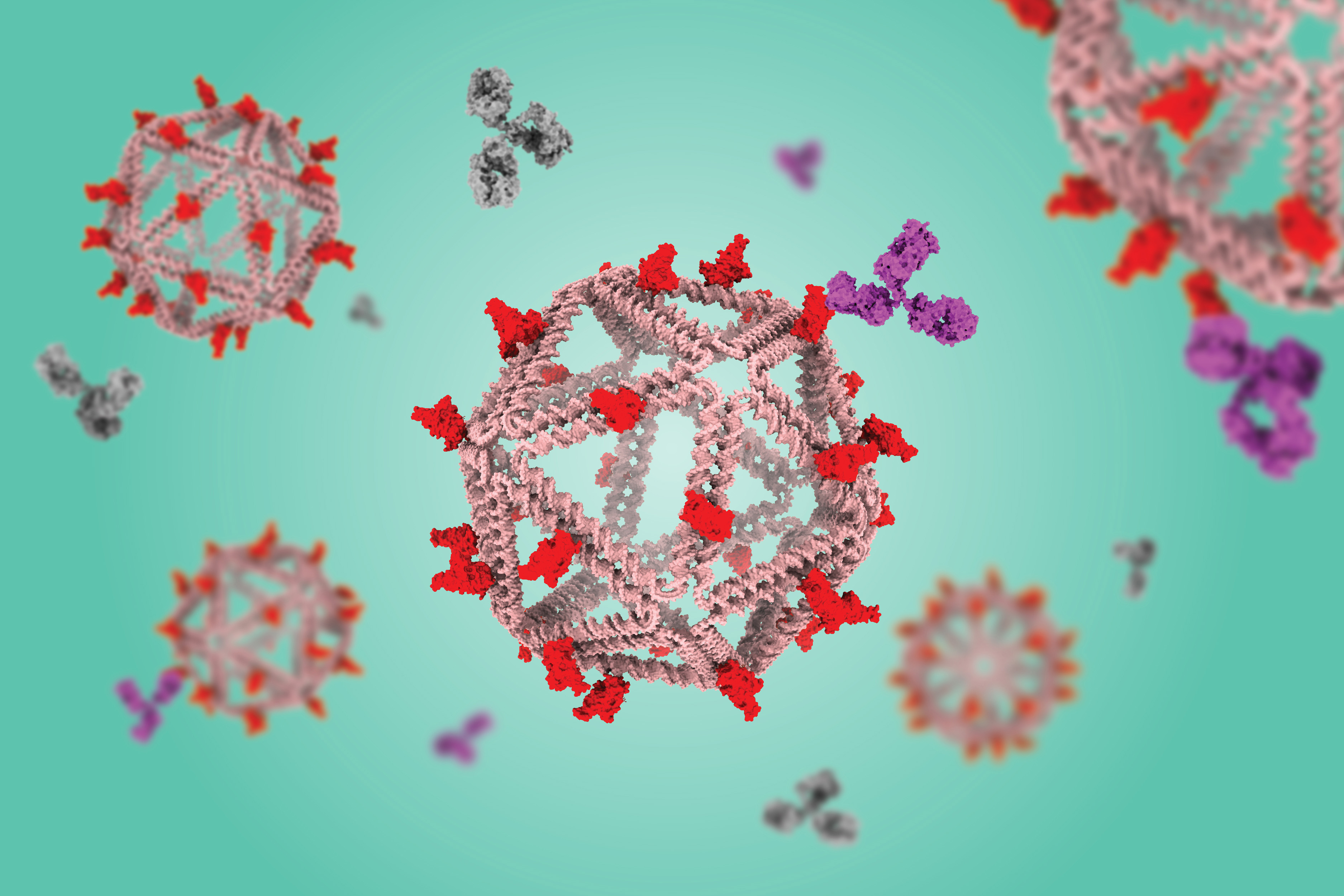
Using a virus-like delivery particle made from DNA, researchers from MIT and the Ragon Institute of MGH, MIT, and Harvard have created a vaccine that can induce a strong antibody response against SARS-CoV-2.

The vaccine, which has been tested in mice, consists of a DNA scaffold that carries many copies of a viral antigen. This type of vaccine, known as a particulate vaccine, mimics the structure of a virus. Most previous work on particulate vaccines has relied on protein scaffolds, but the proteins used in those vaccines tend to generate an unnecessary immune response that can distract the immune system from the target.

In the mouse study, the researchers found that the DNA scaffold does not induce an immune response, allowing the immune system to focus its antibody response on the target antigen.

“DNA, we found in this work, does not elicit antibodies that may distract away from the protein of interest,” says Mark Bathe, an MIT professor of biological engineering. “What you can imagine is that your B cells and immune system are being fully trained by that target antigen, and that’s what you want — for your immune system to be laser-focused on the antigen of interest.”

This approach, which strongly stimulates B cells (the cells that produce antibodies), could make it easier to develop vaccines against viruses that have been difficult to target, including HIV and influenza, as well as SARS-CoV-2, the researchers say. Unlike T cells, which are stimulated by other types of vaccines, these B cells can persist for decades, offering long-term protection.

“We’re interested in exploring whether we can teach the immune system to deliver higher levels of immunity against pathogens that resist conventional vaccine approaches, like flu, HIV, and SARS-CoV-2,” says Daniel Lingwood, an associate professor at Harvard Medical School and a principal investigator at the Ragon Institute. “This idea of decoupling the response against the target antigen from the platform itself is a potentially powerful immunological trick that one can now bring to bear to help those immunological targeting decisions move in a direction that is more focused.”

Bathe, Lingwood, and Aaron Schmidt, an associate professor at Harvard Medical School and principal investigator at the Ragon Institute, are the senior authors of the paper, which appears today in Nature Communications. The paper’s lead authors are Eike-Christian Wamhoff, a former MIT postdoc; Larance Ronsard, a Ragon Institute postdoc; Jared Feldman, a former Harvard University graduate student; Grant Knappe, an MIT graduate student; and Blake Hauser, a former Harvard graduate student. 

Mimicking viruses

Particulate vaccines usually consist of a protein nanoparticle, similar in structure to a virus, that can carry many copies of a viral antigen. This high density of antigens can lead to a stronger immune response than traditional vaccines because the body sees it as similar to an actual virus. Particulate vaccines have been developed for a handful of pathogens, including hepatitis B and human papillomavirus, and a particulate vaccine for SARS-CoV-2 has been approved for use in South Korea.

These vaccines are especially good at activating B cells, which produce antibodies specific to the vaccine antigen.

“Particulate vaccines are of great interest for many in immunology because they give you robust humoral immunity, which is antibody-based immunity, which is differentiated from the T-cell-based immunity that the mRNA vaccines seem to elicit more strongly,” Bathe says.

A potential drawback to this kind of vaccine, however, is that the proteins used for the scaffold often stimulate the body to produce antibodies targeting the scaffold. This can distract the immune system and prevent it from launching as robust a response as one would like, Bathe says.

“To neutralize the SARS-CoV-2 virus, you want to have a vaccine that generates antibodies toward the receptor binding domain portion of the virus’ spike protein,” he says. “When you display that on a protein-based particle, what happens is your immune system recognizes not only that receptor binding domain protein, but all the other proteins that are irrelevant to the immune response you’re trying to elicit.”

Another potential drawback is that if the same person receives more than one vaccine carried by the same protein scaffold, for example, SARS-CoV-2 and then influenza, their immune system would likely respond right away to the protein scaffold, having already been primed to react to it. This could weaken the immune response to the antigen carried by the second vaccine.

“If you want to apply that protein-based particle to immunize against a different virus like influenza, then your immune system can be addicted to the underlying protein scaffold that it’s already seen and developed an immune response toward,” Bathe says. “That can hypothetically diminish the quality of your antibody response for the actual antigen of interest.”

As an alternative, Bathe’s lab has been developing scaffolds made using DNA origami, a method that offers precise control over the structure of synthetic DNA and allows researchers to attach a variety of molecules, such as viral antigens, at specific locations.

In a 2020 study, Bathe and Darrell Irvine, an MIT professor of biological engineering and of materials science and engineering, showed that a DNA scaffold carrying 30 copies of an HIV antigen could generate a strong antibody response in B cells grown in the lab. This type of structure is optimal for activating B cells because it closely mimics the structure of nano-sized viruses, which display many copies of viral proteins in their surfaces.

“This approach builds off of a fundamental principle in B-cell antigen recognition, which is that if you have an arrayed display of the antigen, that promotes B-cell responses and gives better quantity and quality of antibody output,” Lingwood says.

“Immunologically silent”

In the new study, the researchers swapped in an antigen consisting of the receptor binding protein of the spike protein from the original strain of SARS-CoV-2. When they gave the vaccine to mice, they found that the mice generated high levels of antibodies to the spike protein but did not generate any to the DNA scaffold.

In contrast, a vaccine based on a scaffold protein called ferritin, coated with SARS-CoV-2 antigens, generated many antibodies against ferritin as well as SARS-CoV-2.

“The DNA nanoparticle itself is immunogenically silent,” Lingwood says. “If you use a protein-based platform, you get equally high titer antibody responses to the platform and to the antigen of interest, and that can complicate repeated usage of that platform because you’ll develop high affinity immune memory against it.”

Reducing these off-target effects could also help scientists reach the goal of developing a vaccine that would induce broadly neutralizing antibodies to any variant of SARS-CoV-2, or even to all sarbecoviruses, the subgenus of virus that includes SARS-CoV-2 as well as the viruses that cause SARS and MERS.

To that end, the researchers are now exploring whether a DNA scaffold with many different viral antigens attached could induce broadly neutralizing antibodies against SARS-CoV-2 and related viruses. 

The research was primarily funded by the National Institutes of Health, the National Science Foundation, and the Fast Grants program.

© Credit: The Bathe Lab

The vaccine consists of a DNA scaffold that carries many copies of a viral antigen. This type of vaccine, known as a particulate vaccine, mimics the structure of a virus.

Middle-school students meet a beam of electrons, and excitement results

Want to get middle-school kids excited about science? Let them do their own experiments on MIT.nano’s state-of-the-art microscopes — with guidelines and adult supervision, of course. That was the brainchild of Carl Thrasher and Tao Cai, MIT graduate students who spearheaded the Electron Microscopy Elevating Representation and Growth in Education (EMERGE) program.

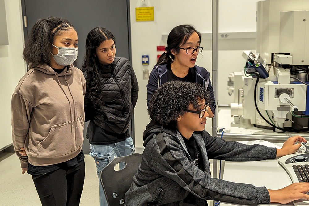
Held in November, EMERGE invited 18 eighth-grade students to the pilot event at MIT.nano, an interdisciplinary facility for nanoscale research, to get hands-on experience in microscopy and materials science.

The highlight of the two-hour workshop: Each student explored mystery samples of everyday materials using one of two scanning electron microscopes (SEMs), which scan material samples using a beam of electrons to form an image. Though highly sophisticated, the instruments generated readily understandable data — images of intricate structures in a butterfly wing or a strand of hair, for example.

The students had an immediate, tangible sense of success, says Thrasher, from MIT’s Department of Materials Science and Engineering (DMSE). He led the program along with Cai, also from DMSE, and Collette Gordon, a grad student in the Department of Chemistry.

“This experience helped build a sense of agency and autonomy around this area of science, nurturing budding self-confidence among the students,” Thrasher says. “We didn’t give the students instructions, just empowered them to solve problems. When you don’t tell them the solution, you get really surprised with what they come up with.”

Unlocking interest in the infinitesimal

The students were part of a multi-year science and engineering exploration program called MITES Saturdays, run by MIT Introduction to Technology, Engineering, and Science, or MITES. A team of volunteers was on hand to help students follow the guidance set out by Thrasher, ensuring the careful handling of the SEMs — worth roughly $500,000 each.

MITES Saturdays program administrator Lynsey Ford was thrilled to observe the students’ autonomous exploration and enthusiasm.

“Our students got to meet real scientists who listened to them, cared about the questions they were asking, and welcomed them into a world of science,” Ford says. “A supportive learning environment can be just as powerful for science discovery as a half-million-dollar microscope.”

The pilot workshop was the first step for Thrasher and his team in their goal to build EMERGE into a program with broad impact, engaging middle-to-high school students from a variety of communities.

The partnership with MITES Saturdays is crucial for this endeavor, says Thrasher, providing a platform to reach a wider audience. “Seeing students from diverse backgrounds participating in EMERGE reinforces the profound difference science education can have.”

MITES Saturdays students are high-achieving Massachusetts seventh through 12th graders from Boston, MIT’s hometown of Cambridge, and nearby Lawrence.

“The majority of students who participate in our programs would be the first person in their family to go to college. A lot of them are from families balancing some sort of financial hardship, and from populations that are historically underrepresented in STEM,” Ford says.

Experienced SEM users set up the instruments and prepared test samples so students could take turns exploring specimens such as burrs, butterfly wings, computer chips, hair, and pollen by operating the microscope to adjust magnification, focus, and stage location.

Students left the EMERGE event with copies of the electron microscope images they generated. Thrasher hopes they will use these materials in follow-up projects, ideally integrating them into existing school curricula so students can share their experiences.

EMERGE co-director Cai says students were excited with their experimentation, both in being able to access such high-end equipment and in seeing what materials like Velcro look like under an SEM (spoiler alert: it’s spaghetti).

“We definitely saw a spark,” Cai says. “The subject matter was complex, but the students always wanted to know more.” And the after-program feedback was positive, with most saying the experience was fun and challenging. The volunteers noted how engaged the students were with the SEMs and subject matter. One volunteer overheard students say, “I felt like a real scientist!”

Inspiring tomorrow’s scientists

EMERGE is based on the Scanning Electron Microscopy Educators program, a long-running STEM outreach program started in 1991 by the Air Force Research Laboratory and adopted by Michigan State University. As an Air Force captain stationed at Wright-Patterson Air Force Base in Ohio, Thrasher participated in the program as a volunteer SEM expert.

“I thought it was an incredible opportunity for young students and wanted to bring it here to MIT,” he says.

The pilot was made possible thanks to support from the MITES Saturdays team and the Graduate Materials Council (GMC), the DMSE graduate student organization. Cai and DMSE grad student Jessica Dong, who are both GMC outreach chairs, helped fund, organize, and coordinate the event.

The MITES Saturdays students included reflections on their experience with the SEMs in their final presentations at the MITES Fall Symposium in November.

“My favorite part of the semester was using the SEM as it introduced me to microscopy at the level of electrons,” said one student.

“Our students had an incredible time with the EMERGE team. We’re excited about the possibility of future partnerships with MIT.nano and other departments at MIT, giving our scholars exposure to the breadth of opportunities as future scientists,” says Eboney Hearn, MITES executive director.

With the success of the pilot, the EMERGE team is looking to offer more programs to the MITES students in the spring. Anna Osherov is excited to give students more access to the cumulative staff knowledge and cutting-edge equipment at MIT.nano, which opened in 2018. Osherov is associate director for Characterization.nano, a shared experimental facility for advanced imaging and analysis.

“Our mission is to support mature researchers — and to help inspire the future PhDs and professors who will come to MIT to learn, research, and innovate,” Osherov says. “Designing and offering such programs, aimed at fostering natural curiosity and creativity of young minds, has a tremendous long-term benefit to our society. We can raise tomorrow’s generation in a better way.”

For her part, Ford is still coasting on the students’ excitement. “They come into the program so curious and hungry for knowledge. They remind me every day how amazing the world is.”

© Photo courtesy of the EMERGE program.

Middle schoolers in the MITES Saturdays science program at MIT examine images of material samples through a scanning electron microscope at MIT.nano, with the help of Rebecca Li (third from left), a postdoc in the Department of Materials Science and Engineering. The students participated in a pilot education program called EMERGE aimed at engaging students in hands-on scientific exploration.

Benchtop test quickly identifies extremely impact-resistant materials

An intricate, honeycomb-like structure of struts and beams could withstand a supersonic impact better than a solid slab of the same material. What’s more, the specific structure matters, with some being more resilient to impacts than others.

That’s what MIT engineers are finding in experiments with microscopic metamaterials — materials that are intentionally printed, assembled, or otherwise engineered with microscopic architectures that give the overall material exceptional properties.

In a study appearing today in the Proceedings of the National Academy of Sciences, the engineers report on a new way to quickly test an array of metamaterial architectures and their resilience to supersonic impacts.

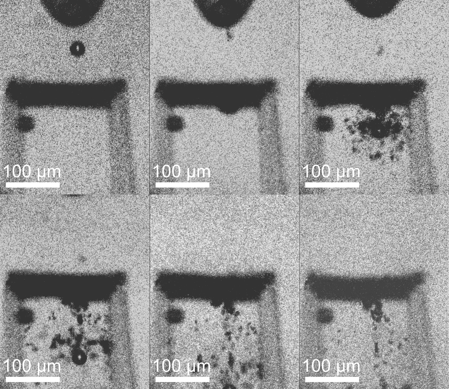
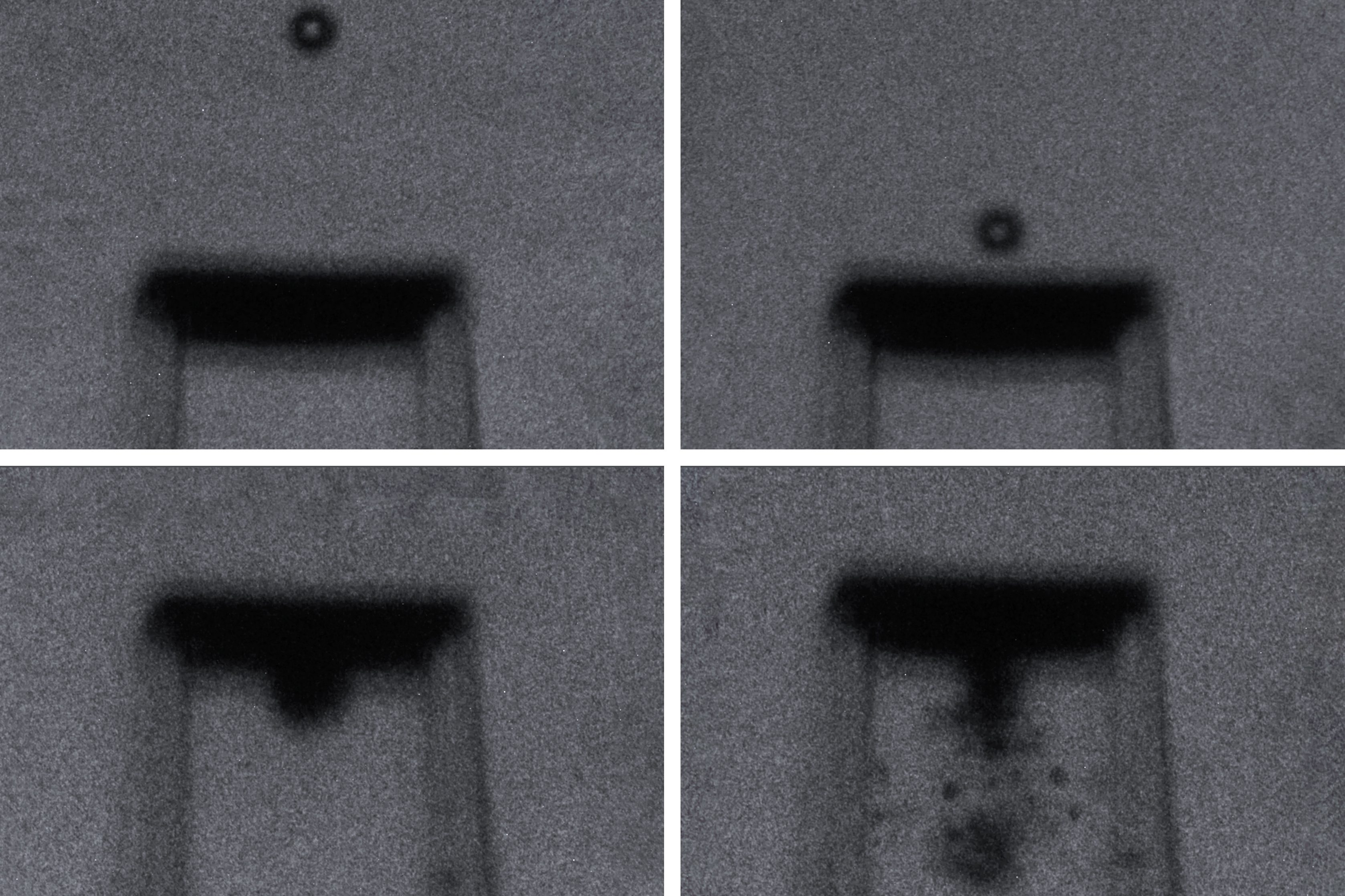
In their experiments, the team suspended tiny printed metamaterial lattices between microscopic support structures, then fired even tinier particles at the materials, at supersonic speeds. With high-speed cameras, the team then captured images of each impact and its aftermath, with nanosecond precision.

Animation of spherical particle smashing through bridge.

Their work has identified a few metamaterial architectures that are more resilient to supersonic impacts compared to their entirely solid, nonarchitected counterparts. The researchers say the results they observed at the microscopic level can be extended to comparable macroscale impacts, to predict how new material structures across length scales will withstand impacts in the real world.

“What we’re learning is, the microstructure of your material matters, even with high-rate deformation,” says study author Carlos Portela, the Brit and Alex d’Arbeloff Career Development Professor in Mechanical Engineering at MIT. “We want to identify impact-resistant structures that can be made into coatings or panels for spacecraft, vehicles, helmets, and anything that needs to be lightweight and protected.”

Other authors on the study include first author and MIT graduate student Thomas Butruille, and Joshua Crone of DEVCOM Army Research Laboratory.

Pure impact

The team’s new high-velocity experiments build off their previous work, in which the engineers tested the resilience of an ultralight, carbon-based material. That material, which was thinner than the width of a human hair, was made from tiny struts and beams of carbon, which the team printed and placed on a glass slide. They then fired microparticles toward the material, at velocities exceeding the speed of sound.  

Those supersonic experiments revealed that the microstructured material withstood the high-velocity impacts, sometimes deflecting the microparticles and other times capturing them.

“But there were many questions we couldn’t answer because we were testing the materials on a substrate, which may have affected their behavior,” Portela says.

In their new study, the researchers developed a way to test freestanding metamaterials, to observe how the materials withstand impacts purely on their own, without a backing or supporting substrate.

In their current setup, the researchers suspend a metamaterial of interest between two microscopic pillars made from the same base material. Depending on the dimensions of the metamaterial being tested, the researchers calculate how far apart the pillars must be in order to support the material at either end while allowing the material to respond to any impacts, without any influence from the pillars themselves.

“This way, we ensure that we’re measuring the material property and not the structural property,” Portela says.

Once the team settled on the pillar support design, they moved on to test a variety of metamaterial architectures. For each architecture, the researchers first printed the supporting pillars on a small silicon chip, then continued printing the metamaterial as a suspended layer between the pillars.

“We can print and test hundreds of these structures on a single chip,” Portela says.

Punctures and cracks

The team printed suspended metamaterials that resembled intricate honeycomb-like cross-sections. Each material was printed with a specific three-dimensional microscopic architecture, such as a precise scaffold of repeating octets, or more faceted polygons. Each repeated unit measured as small as a red blood cell. The resulting metamaterials were thinner than the width of a human hair.

The researchers then tested each metamaterial’s impact resilience by firing glass microparticles toward the structures, at speeds of up to 900 meters per second (more than 2,000 miles per hour) — well within the supersonic range. They caught each impact on camera and studied the resulting images, frame by frame, to see how the projectiles penetrated each material. Next, they examined the materials under a microscope and compared each impact’s physical aftermath.

“In the architected materials, we saw this morphology of small cylindrical craters after impact,” Portela says. “But in solid materials, we saw a lot of radial cracks and bigger chunks of material that were gouged out.”

Overall, the team observed that the fired particles created small punctures in the latticed metamaterials, and the materials nevertheless stayed intact. In contrast, when the same particles were fired at the same speeds into solid, nonlatticed materials of equal mass, they created large cracks that quickly spread, causing the material to crumble. The microstructured materials, therefore, were more efficient in resisting supersonic impacts as well as protecting against multiple impact events. And in particular, materials that were printed with the repeating octets appeared to be the most hardy.

“At the same velocity, we see the octet architecture is harder to fracture, meaning that the metamaterial, per unit mass, can withstand impacts up to twice as much as the bulk material,” Portela says. “This tells us that there are some architectures that can make a material tougher which can offer better impact protection.”

Going forward, the team plans to use the new rapid testing and analysis method to identify new metamaterial designs, in hopes of tagging architectures that can be scaled up to stronger and lighter protective gear, garments, coatings, and paneling.

“What I’m most excited about is showing we can do a lot of these extreme experiments on a benchtop,” Portela says. “This will significantly accelerate the rate at which we can validate new, high-performing, resilient materials.”

This work was funded, in part, by DEVCOM ARL Army Research Office through the MIT Institute for Soldier Nanotechnologies (ISN), and carried out, in part, using ISN’s and MIT.nano’s facilities. 

© Image: Courtesy of the researchers

By firing microparticles at supersonic speeds, MIT engineers can test the resilience of various metamaterials made from structures as small as a red blood cell. Pictured are four video stills of a microparticle hitting a structure made of metamaterials.

Capsid of HIV-1 behaves like cell’s cargo receptor to enter the nucleus

Retroviruses cannot replicate on their own — they must insert their genetic code into the DNA of a host and exploit the host cell's resources to make more copies of themselves, furthering infection. Some retroviruses only infect cells as they divide, when the nuclear envelope that protects the host's genetic material breaks down, making it easily accessible. HIV-1 is a type of retrovirus, called a lentivirus, that can infect non-dividing cells.

HIV-1 delivers its genome into the nucleus by packaging it into a large, cone-shaped structure called a capsid — but the exact mechanism has remained elusive for decades. Travel through the nuclear envelope occurs through, and is regulated by, nuclear pores, doughnut-shaped protein assemblies. Human cells have about 2,000 nuclear pores perforating the nuclear envelope. Some earlier evidence suggested that the capsid remains intact during its delivery into the nucleus — but this created a dimensional conundrum. The cone-shaped HIV-1 capsid is about 120 nanometers long and 60 nm wide — too large, researchers thought, to fit through the opening of the nuclear pore, measured at only 43 nm wide.

Members of the Schwartz Lab at MIT, in the Department of Biology, became interested in this question when a postdoc in the lab used cryo-electron tomography, slicing up sections of frozen cells to examine structures, to show that nuclear pores in the nuclear envelope are larger than 43nm. They deflate and shrink, it turns out, when removed from their native conditions. In native conditions, the nuclear pore complex is about 60nm wide — wide enough to accommodate the HIV-1 capsid.

Knowing that it could fit, a question remained: How can the capsid navigate the dense mesh of spaghetti-like proteins that act like a sieve in the nuclear pore channel? That spaghetti-like mesh allows small cargo to diffuse through, but prevents large cargo from entering unless it is escorted by proteins called nuclear transport receptors.

In an open-access paper published today in Nature, researchers present evidence that the HIV-1 capsid mimics the cell's transport receptors to traverse the nuclear pore.

To support that conclusion, the researchers showed three things in vitro: that an HIV-1 capsid can deliver cargo through a nuclear pore analog; that the capsid can interact with the sieve of proteins in the nuclear pore channel; and that the capsid targets the nuclear pore in the absence of native transport proteins.

Nuclear transport receptors escort large cargo through the nuclear pore by “batting away” the spaghetti-like mesh of proteins inside the channel — like someone holding your hand and guiding you across a crowded dance floor. The HIV-1 capsid interacts with the spaghetti-like proteins, but its purpose is more like a Trojan horse — the capsid encapsulates the viral cargo, protecting it from detection in the cytoplasm and as it enters the nuclear pore complex.

"What's really amazing about cells is that they are incredibly complex. What's really difficult about studying cells is that they are incredibly complex," jokes co-first author Erika Weiskopf, a graduate student in the Schwartz lab. "Biochemists are constantly trying to find ways to study their system in a simplified context, but still give it a flavor of cell biology."

To do that, the Schwartz lab collaborated with Dirk Görlich, the director of cellular logistics at the Max Planck Institute for Multidisciplinary Sciences. Görlich is a co-senior author on the paper with MIT’s Boris Magasanik Professor of Biology Thomas Schwartz. Görlich's lab has produced concentrated droplets of the spaghetti-like proteins found inside the nuclear pore, and those droplets allow and exclude cargo the same way a nuclear pore will. In experiments, fluorescently-labeled cargo did not enter the droplets, but fluorescently-labeled cargo packaged in an HIV-1 capsid was delivered. This indicated that the capsid could deliver cargo through a nuclear pore. 

Using a biophysical binding assay, the researchers also showed that the HIV-1 capsid interacts with the proteins inside the channel. Different spaghetti-like proteins are found in different channel sections, such as at the cytoplasmic side's entrance or only inside the channel; there are 10 such proteins in human cells. The capsid is a promiscuous binder — it can interact with all the spaghetti-like proteins found in the channel.

The capsid can target the nuclear pore complex even without the cell's transport receptors, indicating that it is not commandeering native transport receptors to find and enter the nuclear pore. The team used a classic assay in the nucleocytoplasmic transport field to collect this evidence: When cells are treated with digitonin, their membranes become porous. Everything in the cytoplasm will leak out of the cells, but the nuclear envelope will remain intact. Despite the absence of native proteins, the capsid was attracted to the nuclear pore complex, a behavior indicative of a nuclear transport receptor.

Although the capsid behaves like a nuclear transport receptor to penetrate the nuclear pore, it is fundamentally different. A transport receptor doesn't need to conceal material for delivery the way the capsid does to avoid detection.

These findings open new lines of inquiry for what the nuclear pore complex is capable of accommodating.

"The HIV-1 capsid is one of the largest things that we now know can go through the nuclear pore complex intact," Weiskopf says. "It raises all kinds of questions — what other things could be going through the pore that we thought was impossible?"

Schwartz said another question is whether all of the 2,000 nuclear pores in human cells are identical or whether there is something that makes certain pores more amenable to allowing the capsid through.

The capsid is also known to be unusually elastic, a property that may be key for passage through the pore. Another interesting question for the field is whether the cone-shaped capsid gains entry into the pore by squeezing through.

Although the team has shown that the capsid can enter the pore, what happens at the other end of the channel is still unknown — whether the capsid fully or partially enters the nucleus or breaks down inside the channel. Weiskopf is working on perturbing parts of the capsid or the spaghetti-like proteins to learn more about which interactions are most important for successful capsid entry.

Although these results have expanded our understanding of the nuclear pore, much remains unknown, both for HIV-1 infection and for the transport process through the nuclear pore complex.  

"The nuclear pore is such an important element of cell biology, we thought it would be interesting to understand it better — and that's how we figured out that the pore is much bigger than we anticipated," Schwartz says. "We will certainly try to see whether we can understand the mechanism of HIV-1 infection, how the capsid is released on the other side of the channel, and what factors are important there — and to what extent you can manipulate it or influence it for therapeutic applications."

This research was carried out, in part, using MIT.nano facilities.

© Image courtesy of the Schwartz Lab.

An HIV-1 capsid penetrates a nuclear pore complex by interacting with the spaghetti-like proteins inside the channel, behaving like the cell’s own cargo transport proteins.

Researchers improve blood tests’ ability to detect and monitor cancer

Tumors constantly shed DNA from dying cells, which briefly circulates in the patient’s bloodstream before it is quickly broken down. Many companies have created blood tests that can pick out this tumor DNA, potentially helping doctors diagnose or monitor cancer or choose a treatment.

The amount of tumor DNA circulating at any given time, however, is extremely small, so it has been challenging to develop tests sensitive enough to pick up that tiny signal. A team of researchers from MIT and the Broad Institute of MIT and Harvard has now come up with a way to significantly boost that signal, by temporarily slowing the clearance of tumor DNA circulating in the bloodstream.

The researchers developed two different types of injectable molecules that they call “priming agents,” which can transiently interfere with the body’s ability to remove circulating tumor DNA from the bloodstream. In a study of mice, they showed that these agents could boost DNA levels enough that the percentage of detectable early-stage lung metastases leapt from less than 10 percent to above 75 percent.

This approach could enable not only earlier diagnosis of cancer, but also more sensitive detection of tumor mutations that could be used to guide treatment. It could also help improve detection of cancer recurrence.

“You can give one of these agents an hour before the blood draw, and it makes things visible that previously wouldn’t have been. The implication is that we should be able to give everybody who’s doing liquid biopsies, for any purpose, more molecules to work with,” says Sangeeta Bhatia, the John and Dorothy Wilson Professor of Health Sciences and Technology and of Electrical Engineering and Computer Science at MIT, and a member of MIT’s Koch Institute for Integrative Cancer Research and the Institute for Medical Engineering and Science.

Bhatia is one of the senior authors of the new study, along with J. Christopher Love, the Raymond A. and Helen E. St. Laurent Professor of Chemical Engineering at MIT and a member of the Koch Institute and the Ragon Institute of MGH, MIT, and Harvard and Viktor Adalsteinsson, director of the Gerstner Center for Cancer Diagnostics at the Broad Institute.

Carmen Martin-Alonso PhD ’23, MIT and Broad Institute postdoc Shervin Tabrizi, and Broad Institute scientist Kan Xiong are the lead authors of the paper, which appears today in Science.

Better biopsies

Liquid biopsies, which enable detection of small quantities of DNA in blood samples, are now used in many cancer patients to identify mutations that could help guide treatment. With greater sensitivity, however, these tests could become useful for far more patients. Most efforts to improve the sensitivity of liquid biopsies have focused on developing new sequencing technologies to use after the blood is drawn.

While brainstorming ways to make liquid biopsies more informative, Bhatia, Love, Adalsteinsson, and their trainees came up with the idea of trying to increase the amount of DNA in a patient’s bloodstream before the sample is taken.

“A tumor is always creating new cell-free DNA, and that’s the signal that we’re attempting to detect in the blood draw. Existing liquid biopsy technologies, however, are limited by the amount of material you collect in the tube of blood,” Love says. “Where this work intercedes is thinking about how to inject something beforehand that would help boost or enhance the amount of signal that is available to collect in the same small sample.”

The body uses two primary strategies to remove circulating DNA from the bloodstream. Enzymes called DNases circulate in the blood and break down DNA that they encounter, while immune cells known as macrophages take up cell-free DNA as blood is filtered through the liver.

The researchers decided to target each of these processes separately. To prevent DNases from breaking down DNA, they designed a monoclonal antibody that binds to circulating DNA and protects it from the enzymes.

“Antibodies are well-established biopharmaceutical modalities, and they’re safe in a number of different disease contexts, including cancer and autoimmune treatments,” Love says. “The idea was, could we use this kind of antibody to help shield the DNA temporarily from degradation by the nucleases that are in circulation? And by doing so, we shift the balance to where the tumor is generating DNA slightly faster than is being degraded, increasing the concentration in a blood draw.”

The other priming agent they developed is a nanoparticle designed to block macrophages from taking up cell-free DNA. These cells have a well-known tendency to eat up synthetic nanoparticles.

“DNA is a biological nanoparticle, and it made sense that immune cells in the liver were probably taking this up just like they do synthetic nanoparticles. And if that were the case, which it turned out to be, then we could use a safe dummy nanoparticle to distract those immune cells and leave the circulating DNA alone so that it could be at a higher concentration,” Bhatia says.

Earlier tumor detection

The researchers tested their priming agents in mice that received transplants of cancer cells that tend to form tumors in the lungs. Two weeks after the cells were transplanted, the researchers showed that these priming agents could boost the amount of circulating tumor DNA recovered in a blood sample by up to 60-fold.

Once the blood sample is taken, it can be run through the same kinds of sequencing tests now used on liquid biopsy samples. These tests can pick out tumor DNA, including specific sequences used to determine the type of tumor and potentially what kinds of treatments would work best.

Early detection of cancer is another promising application for these priming agents. The researchers found that when mice were given the nanoparticle priming agent before blood was drawn, it allowed them to detect circulating tumor DNA in blood of 75 percent of the mice with low cancer burden, while none were detectable without this boost.

“One of the greatest hurdles for cancer liquid biopsy testing has been the scarcity of circulating tumor DNA in a blood sample,” Adalsteinsson says. “It’s thus been encouraging to see the magnitude of the effect we’ve been able to achieve so far and to envision what impact this could have for patients.”

After either of the priming agents are injected, it takes an hour or two for the DNA levels to increase in the bloodstream, and then they return to normal within about 24 hours.

“The ability to get peak activity of these agents within a couple of hours, followed by their rapid clearance, means that someone could go into a doctor’s office, receive an agent like this, and then give their blood for the test itself, all within one visit,” Love says. “This feature bodes well for the potential to translate this concept into clinical use.”

The researchers have launched a company called Amplifyer Bio that plans to further develop the technology, in hopes of advancing to clinical trials.

“A tube of blood is a much more accessible diagnostic than colonoscopy screening or even mammography,” Bhatia says. “Ultimately, if these tools really are predictive, then we should be able to get many more patients into the system who could benefit from cancer interception or better therapy.”

The research was funded by the Koch Institute Support (core) Grant from the National Cancer Institute, the Marble Center for Cancer Nanomedicine, the Gerstner Family Foundation, the Ludwig Center at MIT, the Koch Institute Frontier Research Program via the Casey and Family Foundation, and the Bridge Project, a partnership between the Koch Institute and the Dana-Farber/Harvard Cancer Center.

© Image: MIT News; iStock

A new way to recover significantly more circulating tumor DNA in a blood sample could improve the sensitivity of liquid biopsies used to detect, monitor, and guide treatment of tumors.

Shell joins MIT.nano Consortium

MIT.nano has announced that Shell, a global group of energy and petrochemical companies, has joined the MIT.nano Consortium.

“With an international perspective on the world’s energy challenges, Shell is an exciting addition to the MIT.nano Consortium,” says Vladimir Bulović, the founding faculty director of MIT.nano and the Fariborz Maseeh (1990) Professor of Emerging Technologies. “The quest to build a sustainable energy future will require creative thinking backed by broad and deep expertise that our Shell colleagues bring. They will be insightful collaborators for the MIT community and for our member companies as we work together to explore innovative technology strategies.”

Founded in 1907 when Shell Transport and Trading Co. merged with Royal Dutch, Shell has more than a century’s worth of experience in the exploration, production, refining, and marketing of oil and natural gas and the manufacturing and marketing of chemicals. Operating in over 70 countries, Shell has set a target to become a net-zero emissions energy business by 2050. To achieve this, Shell is supporting developments of low-carbon energy solutions such as biofuels, hydrogen, charging for electric vehicles, and electricity generated by solar and wind power.

“In line with our Powering Progress strategy, our research efforts to become a net-zero emission energy company by 2050 will require intense collaboration with academic leaders across a wide range of disciplines,” says Rolf van Benthem, Shell’s chief scientist for materials science. “We look forward to engaging with the top-notch PIs [principal investigators] at MIT.nano who excel in fields like materials design and nanoscale characterization for use in energy applications and carbon utilization. Together we can work on truly sustainable solutions for our society.”

Shell has been engaged in research collaborations with MIT since 2002 and is a founding member of the MIT Energy Initiative (MITEI). Recent MIT projects supported by Shell include an urban building energy model with the MIT Sustainable Design Laboratory that explores energy-saving building retrofits, a study of the role and impact of hydrogen-based technology pathways with MITEI, and a materials science and engineering project to design better batteries for electric vehicles.

The MIT.nano Consortium is a platform for academia-industry collaboration centered around research and innovation emerging from nanoscale science and engineering at MIT. Through activities that include quarterly industry consortium meetings, Shell will gain insight into the work of MIT.nano’s community of users and provide advice to help guide and advance nanoscale innovations at MIT alongside the 11 other consortium companies:

  • Analog Devices;
  • Draper;
  • Edwards;
  • Fujikura;
  • IBM Research;
  • Lam Research;
  • NC;
  • NEC;
  • Raith;
  • UpNano; and
  • Viavi Solutions.

MIT.nano continues to welcome new companies as sustaining members. For more details, visit the MIT.nano Consortium page.

© Photo courtesy of MIT.nano.

Left to right: Vladimir Bulović, MIT.nano director and the Fariborz Maseeh (1990) Professor of Emerging Technologies; Rolf van Benthem, Shell chief scientist for materials science - polymers; Alexander van der Made, Shell chief scientist for chemistry; Kelly Gavin, MIT.nano Consortium manager; and Tom Gearty, director of communications and initiatives, MIT.nano.

MIT’s tiny technologies go to Washington

On Nov. 7, a team from the Marble Center for Cancer Nanomedicine at MIT showed a Washington audience several examples of how nanotechnologies developed at the Institute can transform the detection and treatment of cancer and other diseases.

The team was one of 40 innovative groups featured at “American Possibilities: A White House Demo Day.” Technology on view spanned energy, artificial intelligence, climate, and health, highlighting advancements that contribute to building a better future for all Americans.

Participants included President Joe Biden, Biden-Harris administration leaders and White House staff, members of Congress, federal R&D funding agencies, scientists and engineers, academics, students, and science and technology industry innovators. The event holds special significance for MIT as eight years ago, MIT's Computer Science and Artificial Intelligence Laboratory participated in the last iteration of the White House Demo Day under President Barack Obama.

“It was truly inspirational hearing from experts from all across the government, the private sector, and academia touching on so many fields,” said President Biden of the event. “It was a reminder, at least for me, of what I’ve long believed — that America can be defined by a single word... possibilities.”

Launched in 2016, the Marble Center for Cancer Nanomedicine was established at the Koch Institute for Integrative Research at MIT to serve as a hub for miniaturized biomedical technologies, especially those that address grand challenges in cancer detection, treatment, and monitoring. The center convenes Koch Institute faculty members Sangeeta Bhatia, Paula Hammond, Robert Langer, Angela Belcher, Darrell Irvine, and Daniel Anderson to advance nanomedicine, as well as to facilitate collaboration with industry partners, including Alloy Therapeutics, Danaher Corp., Fujifilm, and Sanofi. 

Ana Jaklenec, a principal research scientist at the Koch Institute, highlighted several groundbreaking technologies in vaccines and disease diagnostics and treatment at the event. Jaklenec gave demonstrations from projects from her research group, including novel vaccine formulations capable of releasing a dozen booster doses pulsed over predetermined time points, microneedle vaccine technologies, and nutrient delivery technologies for precise control over microbiome modulation and nutrient absorption.

Jaklenec describes the event as “a wonderful opportunity to meet our government leaders and policymakers and see their passion for curing cancer. But it was especially moving to interact with people representing diverse communities across the United States and hear their excitement for how our technologies could positively impact their communities.”

Jeremy Li, a former MIT postdoc, presented a technology developed in the Belcher laboratory and commercialized by the spinout Cision Vision. The startup is developing a new approach to visualize lymph nodes in real time without any injection or radiation. The shoebox-sized device was also selected as part of Time Magazine’s Best Inventions of 2023 and is currently being used in a dozen hospitals across the United States.

“It was a proud moment for Cision Vision to be part of this event and discuss our recent progress in the field of medical imaging and cancer care,” says Li, who is a co-founder and the CEO of CisionVision. “It was a humbling experience for us to hear directly from patient advocates and cancer survivors at the event. We feel more inspired than ever to bring better solutions for cancer care to patients around the world.”

Other technologies shown at the event included new approaches such as a tortoise-shaped pill designed to enhance the efficacy of oral medicines, a miniature organ-on-a-chip liver device to predict drug toxicity and model liver disease, and a wireless bioelectronic device that provides oxygen for cell therapy applications and for the treatment of chronic disease.

“The feedback from the organizers and the audience at the event has been overwhelmingly positive,” says Tarek Fadel, who led the team’s participation at the event. “Navigating the demonstration space felt like stepping into the future. As a center, we stand poised to engineer transformative tools that will truly make a difference for the future of cancer care.”

Sangeeta Bhatia, the Director of the Marble Center and the John J. and Dorothy Wilson Professor of Health Sciences and Technology and Electrical Engineering and Computer Science, adds: “The showcase of our technologies at the White House Demo Day underscores the transformative impact we aim to achieve in cancer detection and treatment. The event highlights our vision to advance cutting-edge solutions for the benefit of patients and communities worldwide.”

Ana Jaklenec (right), principal research scientist at the Koch Institute for Integrative Cancer Research at MIT, and Jeremy Li, CEO and co-founder of Cision Vision, presented at “American Possibilities: A White House Demo Day.”

Nanoparticle-delivered RNA reduces neuroinflammation in lab tests

Some Covid-19 vaccines safely and effectively used lipid nanoparticles (LNPs) to deliver messenger RNA to cells. A new MIT study shows that different nanoparticles could be used for a potential Alzheimer’s disease (AD) therapy. In tests in multiple mouse models and with cultured human cells, a newly tailored LNP formulation effectively delivered small interfering RNA (siRNA) to the brain’s microglia immune cells to suppress expression of a protein linked to excessive inflammation in Alzheimer’s disease.

In a prior study, the researchers showed that blocking the consequences of PU.1 protein activity helps to reduce Alzheimer’s disease-related neuroinflammation and pathology. The new open-access results, reported in the journal Advanced Materials, achieves a reduction in inflammation by directly tamping down expression of the Spi1 gene that encodes PU.1. More generally, the new study also demonstrates a new way to deliver RNA to microglia, which have been difficult to target so far.

Study co-senior author Li-Huei Tsai, the Picower professor of neuroscience and director of The Picower Institute for Learning and Memory and Aging Brain Initiative at MIT, says she hypothesized that LNPs might work as a way to bring siRNA into microglia because the cells, which clear waste in the brain, have a strong proclivity to uptake lipid molecules. She discussed this with Robert Langer, the David Koch Institute Professor, who is widely known for his influential work on nanoparticle drug delivery. They decided to test the idea of reducing PU.1 expression with an LNP-delivered siRNA.

“I still remember the day when I asked to meet with Bob to discuss the idea of testing LNPs as a payload to target inflammatory microglia,” says Tsai, a faculty member in the Department of Brain and Cognitive Sciences. “I am very grateful to The JPB Foundation, who supported this idea without any preliminary evidence.”

Langer Lab graduate student Jason Andresen and former Tsai Lab postdoc William Ralvenius led the work and are the study’s co-lead authors. Owen Fenton, a former Langer Lab postdoc who is now an assistant professor at the University of North Carolina’s Eshelman School of Pharmacy, is a co-corresponding author along with Tsai and Langer. Langer is a professor in the departments of Chemical Engineering and Biological Engineering, and the Koch Institute for Integrative Cancer Research.

Perfecting a particle

The simplest way to test whether siRNA could therapeutically suppress PU.1 expression would have been to make use of an already available delivery device, but one of the first discoveries in the study is that none of eight commercially available reagents could safely and effectively transfect cultured human microglia-like cells in the lab.

Instead, the team had to optimize an LNP to do the job. LNPs have four main components; by changing the structures of two of them, and by varying the ratio of lipids to RNA, the researchers were able to come up with seven formulations to try. Importantly, their testing included trying their formulations on cultured microglia that they had induced into an inflammatory state. That state, after all, is the one in which the proposed treatment is needed.

Among the seven candidates, one the team named “MG-LNP” stood out for its especially high delivery efficiency and safety of a test RNA cargo.

What works in a dish sometimes doesn’t work in a living organism, so the team next tested their LNP formulations’ effectiveness and safety in mice. Testing two different methods of injection, into the body or into the cerebrospinal fluid (CSF), they found that injection into the CSF ensured much greater efficacy in targeting microglia without affecting cells in other organs. Among the seven formulations, MG-LNP again proved the most effective at transfecting microglia. Langer said he believes this could potentially open new ways of treating certain brain diseases with nanoparticles someday. 

A targeted therapy

Once they knew MG-LNP could deliver a test cargo to microglia both in human cell cultures and mice, the scientists then tested whether using it to deliver a PU.1-suppressing siRNA could reduce inflammation in microglia. In the cell cultures, a relatively low dose achieved a 42 percent reduction of PU.1 expression (which is good because microglia need at least some PU.1 to live). Indeed, MG-LNP transfection did not cause the cells any harm. It also significantly reduced the transcription of the genes that PU.1 expression increases in microglia, indicating that it can reduce multiple inflammatory markers.

In all these measures, and others, MG-LNP outperformed a commercially available reagent called RNAiMAX that the scientists tested in parallel.

“These findings support the use of MG-LNP-mediated anti-PU.1 siRNA delivery as a potential therapy for neuroinflammatory diseases,” the researchers wrote.

The final set of tests evaluated MG-LNP’s performance delivering the siRNA in two mouse models of inflammation in the brain. In one, mice were exposed to LPS, a molecule that simulates infection and stimulates a systemic inflammation response. In the other model, mice exhibit severe neurodegeneration and inflammation when an enzyme called CDK5 becomes hyperactivated by a protein called p25.

In both models, injection of MG-LNPs carrying the anti-PU.1 siRNA reduced expression of PU.1 and inflammatory markers, much like in the cultured human cells.

“MG-LNP delivery of anti-PU.1 siRNA can potentially be used as an anti-inflammatory therapeutic in mice with systemic inflammation an in the CK-p25 mouse model of AD-like neuroinflammation,” the scientists concluded, calling the results a “proof-of-principle.” More testing will be required before the idea could be tried in human patients.

In addition to Andresen, Ralvenius, Langer, Tsai, and Owen, the paper’s other authors are Margaret Huston, Jay Penney, and Julia Maeve Bonner.

In addition to the The JPB Foundation and The Picower Institute for Learning and Memory, the Robert and Renee Belfer Family, Eduardo Eurnekian, Lester A. Gimpelson, Jay L. and Carroll Miller, the Koch Institute, the Swiss National Science Foundation, and the Alzheimer’s Association provided funding for the study.

© Image courtesy of the Tsai and Langer labs.

In the brain's immune cells, called microglia, the gene product PU.1 is associated with excessive inflammation in neurological disorders such as Alzheimer's disease. MIT researchers delivered a small interfering RNA (siRNA) via lipid nanoparticles to reduce expression of PU.1 in mice. Microglia stained for PU.1 or related markers are less evident in the bottom row, which reflects the effects of the siRNA, compared to an experimental control (top row).

Angela Belcher delivers 2023 Dresselhaus Lecture on evolving organisms for new nanomaterials

“How do we get to making nanomaterials that haven’t been evolved before?” asked Angela Belcher at the 2023 Mildred S. Dresselhaus Lecture at MIT on Nov. 20. “We can use elements that biology has already given us.”

The combined in-person and virtual audience of over 300 was treated to a light-up, 3D model of M13 bacteriophage, a virus that only infects bacteria, complete with a pull-out strand of DNA. Belcher used the feather-boa-like model to show how her research group modifies the M13’s genes to add new DNA and peptide sequences to template inorganic materials.

“I love controlling materials at the nanoscale using biology,” said Belcher, the James Mason Crafts Professor of Biological Engineering, materials science professor, and of the Koch Institute of Integrative Cancer Research at MIT. “We all know if you control materials at the nanoscale and you can start to tune them, then you can have all kinds of different applications.” And the opportunities are indeed vast — from building batteries, fuel cells, and solar cells to carbon sequestration and storage, environmental remediation, catalysis, and medical diagnostics and imaging.

Belcher sprinkled her talk with models and props, lined up on a table at the front of the 10-250 lecture hall, to demonstrate a wide variety of concepts and projects made possible by the intersection of biology and nanotechnology.

Energy storage and environment

“How do you go from a DNA sequence to a functioning battery?” posed Belcher. Grabbing a model of a large carbon nanotube, she explained how her group engineered a phage to pick up carbon nanotubes that would wind all the way around the virus and then fill in with different cathode or anode materials to make nanowires for battery electrodes.

How about using the M13 bacteriophage to improve the environment? Belcher referred to a project by former student Geran Zhang PhD ’19 that proved the virus can be modified for this context, too. He used the phage to template high-surface-area, carbon-based materials that can grab small molecules and break them down, Belcher said, opening a realm of possibilities from cleaning up rivers to developing chemical warfare agents to combating smog.

Belcher’s lab worked with the U.S. Army to produce protective clothing and masks made of these carbon-based virus nanofibers. “We went from five liters in our lab to a thousand liters, then 10,000 liters in the army labs where we’re able to make kilograms of the material,” Belcher said, stressing the importance of being able to test and prototype at scale.

Imaging tools and therapeutics in cancer

In the area of biomedical imaging, Belcher explained, a lot less is known in near-infrared imaging — imaging in wavelengths above 1,000 nanometers — than other imaging techniques, yet with near-infrared scientists can see much deeper inside the body. Belcher’s lab built their own systems to image at these wavelengths. The third generation of this system provides real-time, sub-millimeter optical imaging for guided surgery.

Working with Sangeeta Bhatia, the John J. and Dorothy Wilson Professor of Engineering, Belcher used carbon nanotubes to build imaging tools that find tiny tumors during surgery that doctors otherwise would not be able to see. The tool is actually a virus engineered to carry with it a fluorescent, single-walled carbon nanotube as it seeks out the tumors.

Nearing the end of her talk, Belcher presented a goal: to develop an accessible detection and diagnostic technology for ovarian cancer in five to 10 years.

“We think that we can do it,” Belcher said. She described her students’ work developing a way to scan an entire fallopian tube, as opposed to just one small portion, to find pre-cancer lesions, and talked about the team of MIT faculty, doctors, and researchers working collectively toward this goal.

“Part of the secret of life and the meaning of life is helping other people enjoy the passage of time,” said Belcher in her closing remarks. “I think that we can all do that by working to solve some of the biggest issues on the planet, including helping to diagnose and treat ovarian cancer early so people have more time to spend with their family.”

Honoring Mildred S. Dresselhaus

Belcher was the fifth speaker to deliver the Dresselhaus Lecture, an annual event organized by MIT.nano to honor the late MIT physics and electrical engineering Institute Professor Mildred Dresselhaus. The lecture features a speaker from anywhere in the world whose leadership and impact echo Dresselhaus’s life, accomplishments, and values.

“Millie was and is a huge hero of mine,” said Belcher. “Giving a lecture in Millie’s name is just the greatest honor.”

Belcher dedicated the talk to Dresselhaus, whom she described with an array of accolades — a trailblazer, a genius, an amazing mentor, teacher, and inventor. “Just knowing her was such a privilege,” she said.

Belcher also dedicated her talk to her own grandmother and mother, both of whom passed away from cancer, as well as late MIT professors Susan Lindquist and Angelika Amon, who both died of ovarian cancer.

“I’ve been so fortunate to work with just the most talented and dedicated graduate students, undergraduate students, postdocs, and researchers,” concluded Belcher. “It has been a pure joy to be in partnership with all of you to solve these very daunting problems.”

© Photo: Justin Knight

Professor Angela Belcher pulls a single strand of DNA out of a light-up model of M13 bacteriophage, a virus that only infects bacteria. Belcher’s lab modifies the M13’s genes to add new DNA and peptide sequences to template inorganic materials.

Closing the design-to-manufacturing gap for optical devices

Photolithography involves manipulating light to precisely etch features onto a surface, and is commonly used to fabricate computer chips and optical devices like lenses. But tiny deviations during the manufacturing process often cause these devices to fall short of their designers’ intentions.

To help close this design-to-manufacturing gap, researchers from MIT and the Chinese University of Hong Kong used machine learning to build a digital simulator that mimics a specific photolithography manufacturing process. Their technique utilizes real data gathered from the photolithography system, so it can more accurately model how the system would fabricate a design.

The researchers integrate this simulator into a design framework, along with another digital simulator that emulates the performance of the fabricated device in downstream tasks, such as producing images with computational cameras. These connected simulators enable a user to produce an optical device that better matches its design and reaches the best task performance.

This technique could help scientists and engineers create more accurate and efficient optical devices for applications like mobile cameras, augmented reality, medical imaging, entertainment, and telecommunications. And because the pipeline of learning the digital simulator utilizes real-world data, it can be applied to a wide range of photolithography systems.

“This idea sounds simple, but the reasons people haven’t tried this before are that real data can be expensive and there are no precedents for how to effectively coordinate the software and hardware to build a high-fidelity dataset,” says Cheng Zheng, a mechanical engineering graduate student who is co-lead author of an open-access paper describing the work. “We have taken risks and done extensive exploration, for example, developing and trying characterization tools and data-exploration strategies, to determine a working scheme. The result is surprisingly good, showing that real data work much more efficiently and precisely than data generated by simulators composed of analytical equations. Even though it can be expensive and one can feel clueless at the beginning, it is worth doing.”

Zheng wrote the paper with co-lead author Guangyuan Zhao, a graduate student at the Chinese University of Hong Kong; and her advisor, Peter T. So, a professor of mechanical engineering and biological engineering at MIT. The research will be presented at the SIGGRAPH Asia Conference.

Printing with light

Photolithography involves projecting a pattern of light onto a surface, which causes a chemical reaction that etches features into the substrate. However, the fabricated device ends up with a slightly different pattern because of miniscule deviations in the light’s diffraction and tiny variations in the chemical reaction.

Because photolithography is complex and hard to model, many existing design approaches rely on equations derived from physics. These general equations give some sense of the fabrication process but can’t capture all deviations specific to a photolithography system. This can cause devices to underperform in the real world.

For their technique, which they call neural lithography, the MIT researchers build their photolithography simulator using physics-based equations as a base, and then incorporate a neural network trained on real, experimental data from a user’s photolithography system. This neural network, a type of machine-learning model loosely based on the human brain, learns to compensate for many of the system’s specific deviations.

The researchers gather data for their method by generating many designs that cover a wide range of feature sizes and shapes, which they fabricate using the photolithography system. They measure the final structures and compare them with design specifications, pairing those data and using them to train a neural network for their digital simulator.

“The performance of learned simulators depends on the data fed in, and data artificially generated from equations can’t cover real-world deviations, which is why it is important to have real-world data,” Zheng says.

Dual simulators

The digital lithography simulator consists of two separate components: an optics model that captures how light is projected on the surface of the device, and a resist model that shows how the photochemical reaction occurs to produce features on the surface.

In a downstream task, they connect this learned photolithography simulator to a physics-based simulator that predicts how the fabricated device will perform on this task, such as how a diffractive lens will diffract the light that strikes it.

The user specifies the outcomes they want a device to achieve. Then these two simulators work together within a larger framework that shows the user how to make a design that will reach those performance goals.

“With our simulator, the fabricated object can get the best possible performance on a downstream task, like the computational cameras, a promising technology to make future cameras miniaturized and more powerful. We show that, even if you use post-calibration to try and get a better result, it will still not be as good as having our photolithography model in the loop,” Zhao adds.

They tested this technique by fabricating a holographic element that generates a butterfly image when light shines on it. When compared to devices designed using other techniques, their holographic element produced a near-perfect butterfly that more closely matched the design. They also produced a multilevel diffraction lens, which had better image quality than other devices.

In the future, the researchers want to enhance their algorithms to model more complicated devices, and also test the system using consumer cameras. In addition, they want to expand their approach so it can be used with different types of photolithography systems, such as systems that use deep or extreme ultraviolet light.

This research is supported, in part, by the U.S. National Institutes of Health, Fujikura Limited, and the Hong Kong Innovation and Technology Fund.

The work was carried out, in part, using MIT.nano’s facilities.

© Image: MIT News; iStock

Researchers from MIT and elsewhere created an AI technique that learns to simulate a photolithography system, capturing the tiny deviations the system introduces during manufacturing. This method could enable a researcher to fabricate optical devices that more closely match their design specifications, boosting the accuracy and efficiency of electronics.

3 Questions: Darrell Irvine on making HIV vaccines more powerful

An MIT research team led by Professor Darrell Irvine has developed a novel kind of vaccine adjuvant: a nanoparticle that can help to stimulate the immune system to generate a stronger response to a vaccine. These nanoparticles contain saponin, a compound derived from the bark of the Chilean soapbark tree, along with a molecule called MPLA, each of which helps to activate the immune system.

The adjuvant has been incorporated into an experimental HIV vaccine that has shown promising results in animal studies, and this month, the first human volunteers will receive the vaccine as part of a phase 1 clinical trial run by the Consortium for HIV/AIDS Vaccine Development at the Scripps Research Institute. MIT News spoke with Irvine about why this project required an interdisciplinary approach, and what may lie ahead.

Q: What are the special features of the new nanoparticle adjuvant that help it create a more powerful immune response to vaccination? 

A: Most vaccines, such as the Covid-19 vaccines, are thought to protect us through B cells making protective antibodies. Development of an HIV vaccine has been made challenging by the fact that the B cells that are capable of evolving to produce protective antibodies — called broadly neutralizing antibodies — are very rare in the average person. Vaccine adjuvants are important in this scenario to ensure that when we immunize with an HIV antigen, these rare B cells become activated and get a chance to participate in the immune response.

We particularly discovered that this new adjuvant, which we call SMNP (short for saponin/MPLA nanoparticles), is particularly good at helping more B cells enter germinal centers, the specialized location in lymph nodes where high affinity antibodies are produced. In animal models, SMNP also has shown unique mechanisms of action: Administering antigens with SMNP leads to better antigen delivery to lymph nodes (through increases in lymph flow) and better capture of the antigen by B cells in lymph nodes.

Q: How did your lab, which generally focuses on bioengineering and materials science, end up working on HIV vaccines? What obstacles did you have to overcome in the development of this adjuvant?

A: About 15 years ago, Bruce Walker approached me about getting involved in the HIV vaccine effort, and recruited me to join the Ragon Institute of MGH, MIT, and Harvard as a member of the steering committee. Through the Ragon Institute, I met colleagues in the Scripps Consortium for HIV/AIDS Vaccine Development (CHAVD), and we realized there was a tremendous opportunity to directly contribute to the HIV vaccine challenge, working in partnership with experts in immunogen design, structural biology, and HIV pathogenesis.

As we carried out study after study of SMNP in preclinical animal models, we realized the adjuvant had really amazing effects for promoting anti-HIV antibody responses, and the CHAVD decided this was worth moving forward to testing in humans. A major challenge was transferring the technology out of the lab to synthesize large amounts of the adjuvant under GMP (good manufacturing process) conditions for a clinical trial. The initial contract manufacturing organization (CMO) hired by the consortium to produce SMNP simply couldn’t get a process to work for scalable manufacturing.

Luckily for us, a chemical engineering graduate student, Ivan Pires, whom I co-advise with Paula Hammond, head of MIT’s Department of Chemical Engineering, had developed expertise in one particular processing technique known as tangential flow filtration during his undergraduate training. Leveraging classic chemical engineering skills in thermodynamics and process design, Ivan stepped in and solved the process issues the CMO was facing, allowing the manufacturing to move forward. This to me is what makes MIT great — the ability of our students and postdocs to step up and solve big problems and make big contributions when the need arises.

Q: What other diseases could this approach be useful for? Are there any plans to test it with other types of vaccines?

A: In principle, SMNP may be helpful for any infectious disease vaccine where strong antibody responses are needed. We are currently sharing the adjuvant with about 30 different labs around the world, who are testing it in vaccines against many other pathogens including Epstein-Barr virus, malaria, and influenza. We are hopeful that if SMNP is safe and effective in humans, this will be an adjuvant that can be broadly used in infectious disease trials.

© Photo: Steve Boxall

An MIT research team led by Professor Darrell Irvine has developed a novel kind of vaccine adjuvant: a nanoparticle that can help to stimulate the immune system to generate a stronger response to a vaccine. An HIV vaccine that includes this adjuvant will be tested in clinical trials this month.

Scientists 3D print self-heating microfluidic devices

MIT researchers have used 3D printing to produce self-heating microfluidic devices, demonstrating a technique which could someday be used to rapidly create cheap, yet accurate, tools to detect a host of diseases.

Microfluidics, miniaturized machines that manipulate fluids and facilitate chemical reactions, can be used to detect disease in tiny samples of blood or fluids. At-home test kits for Covid-19, for example, incorporate a simple type of microfluidic.

But many microfluidic applications require chemical reactions that must be performed at specific temperatures. These more complex microfluidic devices, which are typically manufactured in a clean room, are outfitted with heating elements made from gold or platinum using a complicated and expensive fabrication process that is difficult to scale up.

Instead, the MIT team used multimaterial 3D printing to create self-heating microfluidic devices with built-in heating elements, through a single, inexpensive manufacturing process. They generated devices that can heat fluid to a specific temperature as it flows through microscopic channels inside the tiny machine.

Their technique is customizable, so an engineer could create a microfluidic that heats fluid to a certain temperature or given heating profile within a specific area of the device. The low-cost fabrication process requires about $2 of materials to generate a ready-to-use microfluidic.

The process could be especially useful in creating self-heating microfluidics for remote regions of developing countries where clinicians may not have access to the expensive lab equipment required for many diagnostic procedures.

“Clean rooms in particular, where you would usually make these devices, are incredibly expensive to build and to run. But we can make very capable self-heating microfluidic devices using additive manufacturing, and they can be made a lot faster and cheaper than with these traditional methods. This is really a way to democratize this technology,” says Luis Fernando Velásquez-García, a principal scientist in MIT’s Microsystems Technology Laboratories (MTL) and senior author of a paper describing the fabrication technique.

He is joined on the paper by lead author Jorge Cañada Pérez-Sala, an electrical engineering and computer science graduate student. The research will be presented at the PowerMEMS Conference this month.

An insulator becomes conductive

This new fabrication process utilizes a technique called multimaterial extrusion 3D printing, in which several materials can be squirted through the printer’s many nozzles to build a device layer by layer. The process is monolithic, which means the entire device can be produced in one step on the 3D printer, without the need for any post-assembly.

To create self-heating microfluidics, the researchers used two materials — a biodegradable polymer known as polylactic acid (PLA) that is commonly used in 3D printing, and a modified version of PLA.

The modified PLA has mixed copper nanoparticles into the polymer, which converts this insulating material into an electrical conductor, Velásquez-García explains. When electrical current is fed into a resistor composed of this copper-doped PLA, energy is dissipated as heat.

“It is amazing when you think about it because the PLA material is a dielectric, but when you put in these nanoparticle impurities, it completely changes the physical properties. This is something we don’t fully understand yet, but it happens and it is repeatable,” he says.

Using a multimaterial 3D printer, the researchers fabricate a heating resistor from the copper-doped PLA and then print the microfluidic device, with microscopic channels through which fluid can flow, directly on top in one printing step. Because the components are made from the same base material, they have similar printing temperatures and are compatible.

Heat dissipated from the resistor will warm fluid flowing through the channels in the microfluidic.

In addition to the resistor and microfluidic, they use the printer to add a thin, continuous layer of PLA that is sandwiched between them. It is especially challenging to manufacture this layer because it must be thin enough so heat can transfer from the resistor to the microfluidic, but not so thin that fluid could leak into the resistor.

The resulting machine is about the size of a U.S. quarter and can be produced in a matter of minutes. Channels about 500 micrometers wide and 400 micrometers tall are threaded through the microfluidic to carry fluid and facilitate chemical reactions.

Importantly, the PLA material is translucent, so fluid in the device remains visible. Many processes rely on visualization or the use of light to infer what is happening during chemical reactions, Velásquez-García explains.

Customizable chemical reactors

The researchers used this one-step manufacturing process to generate a prototype that could heat fluid by 4 degrees Celsius as it flowed between the input and the output. This customizable technique could enable them to make devices which would heat fluids in certain patterns or along specific gradients.

“You can use these two materials to create chemical reactors that do exactly what you want. We can set up a particular heating profile while still having all the capabilities of the microfluidic,” he says.

However, one limitation comes from the fact that PLA can only be heated to about 50 degrees Celsius before it starts to degrade. Many chemical reactions, such as those used for polymerase chain reaction (PCR) tests, require temperatures of 90 degrees or higher. And to precisely control the temperature of the device, researchers would need to integrate a third material that enables temperature sensing.

In addition to tackling these limitations in future work, Velásquez-García wants to print magnets directly into the microfluidic device. These magnets could enable chemical reactions that require particles to be sorted or aligned.

At the same time, he and his colleagues are exploring the use of other materials that could reach higher temperatures. They are also studying PLA to better understand why it becomes conductive when certain impurities are added to the polymer.

“If we can understand the mechanism that is related to the electrical conductivity of PLA, that would greatly enhance the capability of these devices, but it is going to be a lot harder to solve than some other engineering problems,” he adds.

“In Japanese culture, it’s often said that beauty lies in simplicity. This sentiment is echoed by the work of Cañada and Velasquez-Garcia. Their proposed monolithically 3D-printed microfluidic systems embody simplicity and beauty, offering a wide array of potential derivations and applications that we foresee in the future,” says Norihisa Miki, a professor of mechanical engineering at Keio University in Tokyo, who was not involved with this work.

“Being able to directly print microfluidic chips with fluidic channels and electrical features at the same time opens up very exiting applications when processing biological samples, such as to amplify biomarkers or to actuate and mix liquids. Also, due to the fact that PLA degrades over time, one can even think of implantable applications where the chips dissolve and resorb over time,” adds Niclas Roxhed, an associate professor at Sweden’s KTH Royal Institute of Technology, who was not involved with this study.

This research was funded, in part, by the Empiriko Corporation and a fellowship from La Caixa Foundation.

© Image: Courtesy of the researchers
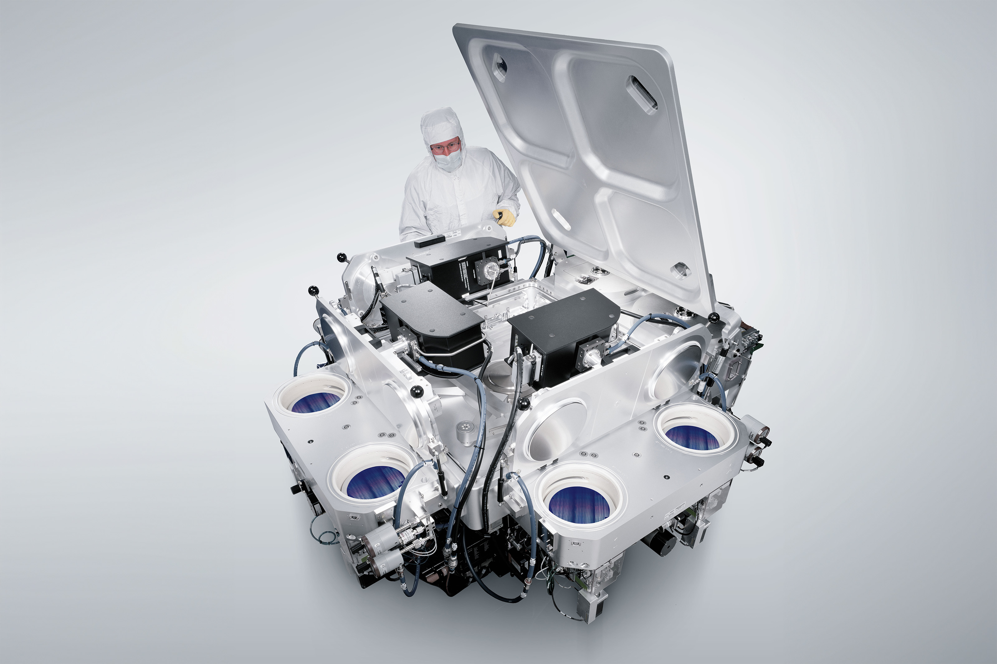
MIT researchers developed a fabrication process to produce self-heating microfluidic devices in one step using a multi-material 3D printer. Pictured is an example of one of the devices.

Researchers safely integrate fragile 2D materials into devices

Two-dimensional materials, which are only a few atoms thick, can exhibit some incredible properties, such as the ability to carry electric charge extremely efficiently, which could boost the performance of next-generation electronic devices.

But integrating 2D materials into devices and systems like computer chips is notoriously difficult. These ultrathin structures can be damaged by conventional fabrication techniques, which often rely on the use of chemicals, high temperatures, or destructive processes like etching.

To overcome this challenge, researchers from MIT and elsewhere have developed a new technique to integrate 2D materials into devices in a single step while keeping the surfaces of the materials and the resulting interfaces pristine and free from defects.

Their method relies on engineering surface forces available at the nanoscale to allow the 2D material to be physically stacked onto other prebuilt device layers. Because the 2D material remains undamaged, the researchers can take full advantage of its unique optical and electrical properties.

They used this approach to fabricate arrays of 2D transistors that achieved new functionalities compared to devices produced using conventional fabrication techniques. Their method, which is versatile enough to be used with many materials, could have diverse applications in high-performance computing, sensing, and flexible electronics.

Core to unlocking these new functionalities is the ability to form clean interfaces, held together by special forces that exist between all matter, called van der Waals forces.

However, such van der Waals integration of materials into fully functional devices is not always easy, says Farnaz Niroui, assistant professor of electrical engineering and computer science (EECS), a member of the Research Laboratory of Electronics (RLE), and senior author of a new paper describing the work.

“Van der Waals integration has a fundamental limit,” she explains. “Since these forces depend on the intrinsic properties of the materials, they cannot be readily tuned. As a result, there are some materials that cannot be directly integrated with each other using their van der Waals interactions alone. We have come up with a platform to address this limit to help make van der Waals integration more versatile, to promote the development of 2D-materials-based devices with new and improved functionalities.”

Niroui wrote the paper with lead author Peter Satterthwaite, an electrical engineering and computer science graduate student; Jing Kong, professor of EECS and a member of RLE; and others at MIT, Boston University, National Tsing Hua University in Taiwan, the National Science and Technology Council of Taiwan, and National Cheng Kung University in Taiwan. The research is published today in Nature Electronics.  

Advantageous attraction

Making complex systems such as a computer chip with conventional fabrication techniques can get messy. Typically, a rigid material like silicon is chiseled down to the nanoscale, then interfaced with other components like metal electrodes and insulating layers to form an active device. Such processing can cause damage to the materials.

Recently, researchers have focused on building devices and systems from the bottom up, using 2D materials and a process that requires sequential physical stacking. In this approach, rather than using chemical glues or high temperatures to bond a fragile 2D material to a conventional surface like silicon, researchers leverage van der Waals forces to physically integrate a layer of 2D material onto a device.

Van der Waals forces are natural forces of attraction that exist between all matter. For example, a gecko’s feet can stick to the wall temporarily due to van der Waals forces. Though all materials exhibit a van der Waals interaction, depending on the material, the forces are not always strong enough to hold them together. For instance, a popular semiconducting 2D material known as molybdenum disulfide will stick to gold, a metal, but won’t directly transfer to insulators like silicon dioxide by just coming into physical contact with that surface.

However, heterostructures made by integrating semiconductor and insulating layers are key building blocks of an electronic device. Previously, this integration has been enabled by bonding the 2D material to an intermediate layer like gold, then using this intermediate layer to transfer the 2D material onto the insulator, before removing the intermediate layer using chemicals or high temperatures.

Instead of using this sacrificial layer, the MIT researchers embed the low-adhesion insulator in a high-adhesion matrix. This adhesive matrix is what makes the 2D material stick to the embedded low-adhesion surface, providing the forces needed to create a van der Waals interface between the 2D material and the insulator.

Making the matrix

To make electronic devices, they form a hybrid surface of metals and insulators on a carrier substrate. This surface is then peeled off and flipped over to reveal a completely smooth top surface that contains the building blocks of the desired device.

This smoothness is important, since gaps between the surface and 2D material can hamper van der Waals interactions. Then, the researchers prepare the 2D material separately, in a completely clean environment, and bring it into direct contact with the prepared device stack.

“Once the hybrid surface is brought into contact with the 2D layer, without needing any high-temperatures, solvents, or sacrificial layers, it can pick up the 2D layer and integrate it with the surface. This way, we are allowing a van der Waals integration that would be traditionally forbidden, but now is possible and allows formation of fully functioning devices in a single step,” Satterthwaite explains.

This single-step process keeps the 2D material interface completely clean, which enables the material to reach its fundamental limits of performance without being held back by defects or contamination.

And because the surfaces also remain pristine, researchers can engineer the surface of the 2D material to form features or connections to other components. For example, they used this technique to create p-type transistors, which are generally challenging to make with 2D materials. Their transistors have improved on previous studies, and can provide a platform toward studying and achieving the performance needed for practical electronics.

Their approach can be done at scale to make larger arrays of devices. The adhesive matrix technique can also be used with a range of materials, and even with other forces to enhance the versatility of this platform. For instance, the researchers integrated graphene onto a device, forming the desired van der Waals interfaces using a matrix made with a polymer. In this case, adhesion relies on chemical interactions rather than van der Waals forces alone.

In the future, the researchers want to build on this platform to enable integration of a diverse library of 2D materials to study their intrinsic properties without the influence of processing damage, and develop new device platforms that leverage these superior functionalities.  

This research is funded, in part, by the U.S. National Science Foundation, the U.S. Department of Energy, the BUnano Cross-Disciplinary Fellowship at Boston University, and the U.S. Army Research Office. The fabrication and characterization procedures were carried out, largely, in the MIT.nano shared facilities.

© Image: Courtesy of Sampson Wilcox/Research Laboratory of Electronics

This artist’s rendition shows a new integration platform developed by MIT researchers. By engineering surface forces, they can directly integrate 2D materials into devices in a single contact-and-release step.

Remembering Professor Judy Hoyt, a pioneer in semiconductor research

Judy Hoyt, a pioneer in semiconductor research and retired MIT professor of electrical engineering and computer science, passed away on Aug. 6. She was 65.

Hoyt is known well for her groundbreaking research on strained silicon semiconductor materials, work which helped greatly decrease the size of integrated circuits. Her most recognized contribution was the first demonstration of the incorporation of lattice strain as a means to enhance performance in scaled silicon devices, a key concept behind the continuation of Moore’s Law roadmap for the last 20 years. This contribution has informed virtually every high-performance chip manufactured today, leading directly to the growth of both the $500 billion semiconductor industry and the multi-trillion-dollar electronics market. 

Hoyt’s contributions earned her the 2011 IEEE Andrew S. Grove Award (together with Eugene Fitzgerald) and the 2018 University Research Award by the Semiconductor Industry Association in collaboration with the Semiconductor Research Corporation. 

Hoyt was a native of Garden City in Long Island, New York. She was not only a talented musician, simultaneously leading her high school band and a swing jazz band, but also a dedicated student, who earned the rank of valedictorian before going on to earn her undergraduate degree in physics and applied mathematics at the University of California at Berkeley in 1980, and her MS and PhD degrees in applied physics at Stanford University in 1983 and 1987, respectively.

After graduation, she stayed on at Stanford as research associate and then senior research associate before joining the faculty of the MIT Department of Electrical Engineering and Computer Science as professor in 2000. From 2005 to 2018, she served as an associate director within the Microsystems Technology Laboratories (MTL) at MIT. She was also an effective proponent and key contributor to the configuration and design of the new MIT.nano building.

Throughout her academic career, Hoyt was a dedicated teacher and mentor to her students at both Stanford and MIT, many of whom went on to distinguished careers in the semiconductor industry. 

Outside of MIT, she was an avid cyclist who loved the outdoors, and animals; her lifelong love of music sustained her as well. 

All at MIT who knew Hoyt will remember her as a gentle soul and a caring friend whose puckish humor and unassuming demeanor hid a stern wisdom, unimpeachable sense of responsibility, and passionate loyalty to her students and her family.

She is survived by sister Barbara, brothers Robert and John, and her father George, as well as longtime close friends and colleagues Conor Rafferty and Dimitri Antoniadis.

Contributions in Hoyt’s memory can be made to St. Jude’s Hospital or the Jimmy Fund in Boston.

© Photo courtesy of Conor Rafferty.

Judy Hoyt, innovator in semiconductors, is remembered warmly by all who knew her at MIT.

A new way to deliver drugs more efficiently

Many of the most promising new pharmaceuticals coming along in the drug development pathway are hydrophobic by nature — that is, they repel water, and are thus hard to dissolve in order to make them available to the body. But now, researchers at MIT have found a more efficient way of processing and delivering these drugs that could make them far more effective.

The new method, which involves initially processing the drugs in a liquid solution rather than in solid form, is reported in a paper in the Dec. 15 print issue of the journal Advanced Healthcare Materials, written by MIT graduate student Lucas Attia, recent graduate Liang-Hsun Chen PhD ’22, and professor of chemical engineering Patrick Doyle.

Currently, much drug processing is done through a long series of sequential steps, Doyle explains. “We think we can streamline the process, but also get better products, by combining these steps and leveraging our understanding of soft matter and self-assembly processes,” he says.

Attia adds that “a lot of small-molecule active ingredients are hydrophobic, so they don’t like being in water and they have very poor dissolution in water, which leads to their poor bioavailability.” Giving such drugs orally, which patients prefer over injections, presents real challenges in getting the material into the patient’s bloodstream. Up to 90 percent of the candidate drug molecules being developed by pharmaceutical companies actually are hydrophobic, he says, “so this is relevant to a large class of potential drug molecules.”

Another advantage of the new process, he says, is that it should make it easier to combine multiple different drugs in a single pill. “For different types of diseases where you’re taking multiple drugs at the same time, this kind of product can be very important in improving patient compliance,” he adds — only having to take one pill instead of a handful makes it much more likely that patients will keep up with their medications. “That’s actually a big issue with these chronic illnesses where patients are on very challenging pill regimes, so combination products have been shown to help a lot.”

One key to the new process is the use of a hydrogel — a sort of sponge-like gel material that can retain water and hold molecules in place. Present processes for making hydrophobic materials more bioavailable involve mechanically grinding the crystals down to smaller size, which makes them dissolve more readily, but this process adds time and expense to the manufacturing process, provides little control over the size distribution of the particles, and can actually damage some more delicate drug molecules.

Instead, the new process involves dissolving the drug in a carrier solution, then generating tiny nanodroplets of this carrier dispersed throughout a polymer solution — a material called a nanoemulsion. Then, this nanoemulsion is squeezed through a syringe and gelled into a hydrogel. The hydrogel holds the droplets in place as the carrier evaporates, leaving behind drug nanocrystals. This approach allows precise control over the final crystal size. The hydrogel, by keeping the droplets in place as they dry, prevents them from simply merging together to form lumpy agglomerations of different sizes. Without the hydrogel the droplets would merge randomly, and “you’d get a mess,” Doyle says. Instead, the new process leaves a batch of perfectly uniform nanoparticles. “That’s a very unique, novel way that our group has invented, to do this sort of crystallization and maintain the nano size,” he says.

The new process yields a two-part package: a core, which contains the active molecules, surrounded by a shell, also made of hydrogel, which can control the timing between ingestion of the pill and the release of its contents into the body.

“We showed that we can get very precise control over the drug release, both in terms of delay and rate,” says Doyle, who is the Robert T. Haslam Professor of Chemical Engineering and Singapore Research Professor. For example, if a drug is targeting disease in the lower intestine or colon, “we can control how long until the drug release starts, and then we also get very fast release once it begins.” Drugs formulated the conventional way with mechanical nanomilling, he says, “would have a slow drug release.”

This process, Attia says, “is the first approach that can form core-shell composite particles and structure drugs in distinct polymeric layers in a single processing step.”

The next steps in developing the process will be to test the system on a wide variety of drug molecules, beyond the two representative examples that were tested so far, Doyle says. Although they have reason to believe the process is generalizable, he says, “the proof is in the pudding — having the data in hand.”

The dripping process they use, he says, “can be scalable, but there’s a lot of details to be worked out.” But because all of the materials they are working with have been chosen as ones that are already recognized as safe for medical use, the approval process should be straightforward, he says. “It could be implemented in a few years. … We’re not worrying about all those typical safety hurdles that I think other novel formulations have to go through, which can be very expensive.”

The work received support from the U.S. Department of Energy.

© Image: Betsy Skrip

The new approach enables programmable drug release for diverse applications in oral delivery, including delayed and sequential release of different hydrophobic actives.

Celebrating five years of MIT.nano

There is vast opportunity for nanoscale innovation to transform the world in positive ways — expressed MIT.nano Director Vladimir Bulović as he posed two questions to attendees at the start of the inaugural Nano Summit: “Where are we heading? And what is the next big thing we can develop?”

“The answer to that puts into perspective our main purpose — and that is to change the world,” Bulović, the Fariborz Maseeh Professor of Emerging Technologies, told an audience of more than 325 in-person and 150 virtual participants gathered for an exploration of nano-related research at MIT and a celebration of MIT.nano’s fifth anniversary.

Over a decade ago, MIT embarked on a massive project for the ultra-small — building an advanced facility to support research at the nanoscale. Construction of MIT.nano in the heart of MIT’s campus, a process compared to assembling a ship in a bottle, began in 2015, and the facility launched in October 2018.

Fast forward five years: MIT.nano now contains nearly 170 tools and instruments serving more than 1,200 trained researchers. These individuals come from over 300 principal investigator labs, representing more than 50 MIT departments, labs, and centers. The facility also serves external users from industry, other academic institutions, and over 130 startup and multinational companies. And in 2022, MIT.nano's home — Building 12 — was named in honor of Lisa T. Su ’90, SM ’91, PhD ’94, chief executive officer and chair of the Board of Directors of AMD.

A cross section of these faculty and researchers joined industry partners and MIT community members to kick off the first Nano Summit, which is expected to become an annual flagship event for MIT.nano and its industry consortium. Held on Oct. 24, the inaugural conference was co-hosted by the MIT Industrial Liaison Program.

Six topical sessions highlighted recent developments in quantum science and engineering, materials, advanced electronics, energy, biology, and immersive data technology. The Nano Summit also featured startup ventures and an art exhibition.

Watch the videos here.

Seeing and manipulating at the nanoscale — and beyond

“We need to develop new ways of building the next generation of materials,” said Frances Ross, the TDK Professor in Materials Science and Engineering (DMSE). “We need to use electron microscopy to help us understand not only what the structure is after it’s built, but how it came to be. I think the next few years in this piece of the nano realm are going to be really amazing.”

Speakers in the session “The Next Materials Revolution,” chaired by MIT.nano co-director for Characterization.nano and associate professor in DMSE James LeBeau, highlighted areas in which cutting-edge microscopy provides insights into the behavior of functional materials at the nanoscale, from anti-ferroelectrics to thin-film photovoltaics and 2D materials. They shared images and videos collected using the instruments in MIT.nano’s characterization suites, which were specifically designed and constructed to minimize mechanical-vibrational and electro-magnetic interference.

Later, in the “Biology and Human Health” session chaired by Boris Magasanik Professor of Biology Thomas Schwartz, biologists echoed the materials scientists, stressing the importance of the ultra-quiet, low-vibration environment in Characterization.nano to obtain high-resolution images of biological structures.

“Why is MIT.nano important for us?” asked Schwartz. “An important element of biology is to understand the structure of biology macromolecules. We want to get to an atomic resolution of these structures. CryoEM (cryo-electron microscopy) is an excellent method for this. In order to enable the resolution revolution, we had to get these instruments to MIT. For that, MIT.nano was fantastic.”

Seychelle Vos, the Robert A. Swanson (1969) Career Development Professor of Life Sciences, shared CryoEM images from her lab’s work, followed by biology Associate Professor Joey Davis who spoke about image processing. When asked about the next stage for CryoEM, Davis said he’s most excited about in-situ tomography, noting that there are new instruments being designed that will improve the current labor-intensive process.

To chart the future of energy, chemistry associate professor Yogi Surendranath is also using MIT.nano to see what is happening at the nanoscale in his research to use renewable electricity to change carbon dioxide into fuel.

“MIT.nano has played an immense role, not only in facilitating our ability to make nanostructures, but also to understand nanostructures through advanced imaging capabilities,” said Surendranath. “I see a lot of the future of MIT.nano around the question of how nanostructures evolve and change under the conditions that are relevant to their function. The tools at MIT.nano can help us sort that out.”

Tech transfer and quantum computing

The “Advanced Electronics” session chaired by Jesús del Alamo, the Donner Professor of Science in the Department of Electrical Engineering and Computer Science (EECS), brought together industry partners and MIT faculty for a panel discussion on the future of semiconductors and microelectronics. “Excellence in innovation is not enough, we also need to be excellent in transferring these to the marketplace,” said del Alamo. On this point, panelists spoke about strengthening the industry-university connection, as well as the importance of collaborative research environments and of access to advanced facilities, such as MIT.nano, for these environments to thrive.

The session came on the heels of a startup exhibit in which eleven START.nano companies presented their technologies in health, energy, climate, and virtual reality, among other topics. START.nano, MIT.nano’s hard-tech accelerator, provides participants use of MIT.nano’s facilities at a discounted rate and access to MIT’s startup ecosystem. The program aims to ease hard-tech startups’ transition from the lab to the marketplace, surviving common “valleys of death” as they move from idea to prototype to scaling up.

When asked about the state of quantum computing in the “Quantum Science and Engineering” session, physics professor Aram Harrow related his response to these startup challenges. “There are quite a few valleys to cross — there are the technical valleys, and then also the commercial valleys.” He spoke about scaling superconducting qubits and qubits made of suspended trapped ions, and the need for more scalable architectures, which we have the ingredients for, he said, but putting everything together is quite challenging.

Throughout the session, William Oliver, professor of physics and the Henry Ellis Warren (1894) Professor of Electrical Engineering and Computer Science, asked the panelists how MIT.nano can address challenges in assembly and scalability in quantum science.

“To harness the power of students to innovate, you really need to allow them to get their hands dirty, try new things, try all their crazy ideas, before this goes into a foundry-level process,” responded Kevin O’Brien, associate professor in EECS. “That’s what my group has been working on at MIT.nano, building these superconducting quantum processors using the state-of-the art fabrication techniques in MIT.nano.”

Connecting the digital to the physical

In his reflections on the semiconductor industry, Douglas Carlson, senior vice president for technology at MACOM, stressed connecting the digital world to real-world application. Later, in the “Immersive Data Technology” session, MIT.nano associate director Brian Anthony explained how, at the MIT.nano Immersion Lab, researchers are doing just that.

“We think about and facilitate work that has the human immersed between hardware, data, and experience,” said Anthony, principal research scientist in mechanical engineering. He spoke about using the capabilities of the Immersion Lab to apply immersive technologies to different areas — health, sports, performance, manufacturing, and education, among others. Speakers in this session gave specific examples in hardware, pediatric health, and opera.

Anthony connected this third pillar of MIT.nano to the fab and characterization facilities, highlighting how the Immersion Lab supports work conducted in other parts of the building. The Immersion Lab’s strength, he said, is taking novel work being developed inside MIT.nano and bringing it up to the human scale to think about applications and uses.

Artworks that are scientifically inspired

The Nano Summit closed with a reception at MIT.nano where guests could explore the facility and gaze through the cleanroom windows, where users were actively conducting research. Attendees were encouraged to visit an exhibition on MIT.nano’s first- and second-floor galleries featuring work by students from the MIT Program in Art, Culture, and Technology (ACT) who were invited to utilize MIT.nano’s tool sets and environments as inspiration for art.

In his closing remarks, Bulović reflected on the community of people who keep MIT.nano running and who are using the tools to advance their research. “Today we are celebrating the facility and all the work that has been done over the last five years to bring it to where it is today. It is there to function not just as a space, but as an essential part of MIT’s mission in research, innovation, and education. I hope that all of us here today take away a deep appreciation and admiration for those who are leading the journey into the nano age.”

© Photo: Jared Charney

MIT faculty and researchers participate in a panel discussion on quantum science and engineering. Left to right: Professor Aram Harrow, Professor Paola Cappellaro, Associate Professor Kevin O'Brien, Research Scientist Jeff Grover, and session chair Professor William Oliver.

Team engineers nanoparticles using ion irradiation to advance clean energy and fuel conversion

MIT researchers and colleagues have demonstrated a way to precisely control the size, composition, and other properties of nanoparticles key to the reactions involved in a variety of clean energy and environmental technologies. They did so by leveraging ion irradiation, a technique in which beams of charged particles bombard a material.

They went on to show that nanoparticles created this way have superior performance over their conventionally made counterparts.

“The materials we have worked on could advance several technologies, from fuel cells to generate CO2-free electricity to the production of clean hydrogen feedstocks for the chemical industry [through electrolysis cells],” says Bilge Yildiz, leader of the work and a professor in MIT’s departments of Nuclear Science and Engineering and Materials Science and Engineering.

Critical catalyst

Fuel and electrolysis cells both involve electrochemical reactions through three principal parts: two electrodes (a cathode and anode) separated by an electrolyte. The difference between the two cells is that the reactions involved run in reverse.

The electrodes are coated with catalysts, or materials that make the reactions involved go faster. But a critical catalyst made of metal-oxide materials has been limited by challenges including low durability. “The metal catalyst particles coarsen at high temperatures, and you lose surface area and activity as a result,” says Yildiz, who is also affiliated with the Materials Research Laboratory and is an author of an open-access paper on the work published in the journal Energy & Environmental Science.

Enter metal exsolution, which involves precipitating metal nanoparticles out of a host oxide onto the surface of the electrode. The particles embed themselves into the electrode, “and that anchoring makes them more stable,” says Yildiz. As a result, exsolution has “led to remarkable progress in clean energy conversion and energy-efficient computing devices,” the researchers write in their paper.

However, controlling the precise properties of the resulting nanoparticles has been difficult. “We know that exsolution can give us stable and active nanoparticles, but the challenging part is really to control it. The novelty of this work is that we’ve found a tool — ion irradiation — that can give us that control,” says Jiayue Wang PhD ’22, first author of the paper. Wang, who conducted the work while earning his PhD in the MIT Department of Nuclear Science and Engineering, is now a postdoc at Stanford University.

Sossina Haile ’86, PhD ’92, the Walter P. Murphy Professor of Materials Science and Engineering at Northwestern University, who was not involved in the current work, says:

“Metallic nanoparticles serve as catalysts in a whole host of reactions, including the important reaction of splitting water to generate hydrogen for energy storage. In this work, Yildiz and colleagues have created an ingenious method for controlling the way that nanoparticles form.”

Haile continues, “the community has shown that exsolution results in structurally stable nanoparticles, but the process is not easy to control, so one doesn’t necessarily get the optimal number and size of particles. Using ion irradiation, this group was able to precisely control the features of the nanoparticles, resulting in excellent catalytic activity for water splitting.”

What they did

The researchers found that aiming a beam of ions at the electrode while simultaneously exsolving metal nanoparticles onto the electrode’s surface allowed them to control several properties of the resulting nanoparticles.

“Through ion-matter interactions, we have successfully engineered the size, composition, density, and location of the exsolved nanoparticles,” the team writes in Energy & Environmental Science.

For example, they could make the particles much smaller — down to 2 billionths of a meter in diameter — than those made using conventional thermal exsolution methods alone. Further, they were able to change the composition of the nanoparticles by irradiating with specific elements. They demonstrated this with a beam of nickel ions that implanted nickel into the exsolved metal nanoparticle. As a result, they demonstrated a direct and convenient way to engineer the composition of exsolved nanoparticles.

“We want to have multi-element nanoparticles, or alloys, because they usually have higher catalytic activity,” Yildiz says. “With our approach, the exsolution target does not have to be dependent on the substrate oxide itself.” Irradiation opens the door to many more compositions. “We can pretty much choose any oxide and any ion that we can irradiate with and exsolve that,” says Yildiz.

The team also found that ion irradiation forms defects in the electrode itself. And these defects provide additional nucleation sites, or places for the exsolved nanoparticles to grow from, increasing the density of the resulting nanoparticles.

Irradiation could also allow extreme spatial control over the nanoparticles. “Because you can focus the ion beam, you can imagine that you could ‘write’ with it to form specific nanostructures,” says Wang. “We did a preliminary demonstration [of that], but we believe it has potential to realize well-controlled micro- and nano-structures.”

The team also showed that the nanoparticles they created with ion irradiation had superior catalytic activity over those created by conventional thermal exsolution alone.

Additional MIT authors of the paper are Kevin B. Woller, a principal research scientist at the Plasma Science and Fusion Center (PSFC), home to the equipment used for ion irradiation; Abinash Kumar PhD ’22, who received his PhD from the Department of Materials Science and Engineering (DMSE) and is now at Oak Ridge National Laboratory; and James M. LeBeau, an associate professor in DMSE. Other authors are Zhan Zhang and Hua Zhou of Argonne National Laboratory, and Iradwikanari Waluyo and Adrian Hunt of Brookhaven National Laboratory.

This work was funded by the OxEon Corp. and MIT’s PSFC. The research also used resources supported by the U.S. Department of Energy Office of Science, MIT’s Materials Research Laboratory, and MIT.nano. The work was performed, in part, at Harvard University through a network funded by the National Science Foundation.

© Image: Jiayue Wang

Artist’s representation of nanoparticles with different compositions created by combining two techniques: metal exsolution and ion irradiation. The different colors represent different elements, such as nickel, that can be implanted into an exsolved metal particle to tailor the particle’s compositions and reactivity.

New laser setup probes metamaterial structures with ultrafast pulses

Metamaterials are products of engineering wizardry. They are made from everyday polymers, ceramics, and metals. And when constructed precisely at the microscale, in intricate architectures, these ordinary materials can take on extraordinary properties.

With the help of computer simulations, engineers can play with any combination of microstructures to see how certain materials can transform, for instance, into sound-focusing acoustic lenses or lightweight, bulletproof films.

But simulations can only take a design so far. To know for sure whether a metamaterial will stand up to expectation, physically testing them is a must. But there’s been no reliable way to push and pull on metamaterials at the microscale, and to know how they will respond, without contacting and physically damaging the structures in the process.

Now, a new laser-based technique offers a safe and fast solution that could speed up the discovery of promising metamaterials for real-world applications.

The technique, developed by MIT engineers, probes metamaterials with a system of two lasers — one to quickly zap a structure and the other to measure the ways in which it vibrates in response, much like striking a bell with a mallet and recording its reverb. In contrast to a mallet, the lasers make no physical contact. Yet they can produce vibrations throughout a metamaterial’s tiny beams and struts, as if the structure were being physically struck, stretched, or sheared.

The engineers can then use the resulting vibrations to calculate various dynamic properties of the material, such as how it would respond to impacts and how it would absorb or scatter sound. With an ultrafast laser pulse, they can excite and measure hundreds of miniature structures within minutes. The new technique offers a safe, reliable, and high-throughput way to dynamically characterize microscale metamaterials, for the first time.

“We need to find quicker ways of testing, optimizing, and tweaking these materials,” says Carlos Portela, the Brit and Alex d’Arbeloff Career Development Professor in Mechanical Engineering at MIT. “With this approach, we can accelerate the discovery of optimal materials, depending on the properties you want.”

Portela and his colleagues detail their new system, which they’ve named LIRAS (for laser-induced resonant acoustic spectroscopy) in a paper appearing today in Nature. His MIT co-authors include first author Yun Kai, Somayajulu Dhulipala, Rachel Sun, Jet Lem, and Thomas Pezeril, along with Washington DeLima at the U.S. Department of Energy’s Kansas City National Security Campus.

Animated drawing of a rectangular tower with a flat top against a white background. The tower is made of an intericate lattice structure, and the top of the tower bends from side to side. When the tower is straight, it is black and white, but as it bends, the areas that are flexed turn green and purple.

A slow tip

The metamaterials that Portela works with are made from common polymers that he 3D-prints into tiny, scaffold-like towers made from microscopic struts and beams. Each tower is patterned by repeating and layering a single geometric unit, such as an eight-pointed configuration of connecting beams. When stacked end to end, the tower arrangement can give the whole polymer properties that it would not otherwise have.

But engineers are severely limited in their options for physically testing and validating these metamaterial properties. Nanoindentation is the typical way in which such microstructures are probed, though in a very deliberate and controlled fashion. The method employs a micrometer-scale tip to slowly push down on a structure while measuring the tiny displacement and forces on the structure as it’s compressed.

“But this technique can only go so fast, while also damaging the structure,” Portela notes. “We wanted to find a way to measure how these structures would behave dynamically, for instance in the initial response to a strong impact, but in a way that would not destroy them.”

A (meta)material world

The team turned to laser ultrasonics — a nondestructive method that uses a short laser pulse tuned to ultrasound frequencies, to excite very thin materials such as gold films without physically touching them. The ultrasound waves created by the laser excitation are within a range that can cause a thin film to vibrate at a frequency that scientists can then use to determine the film’s exact thickness down to nanometer precision. The technique can also be used to determine whether a thin film holds any defects.

Portela and his colleagues realized that ultrasonic lasers might also safely induce their 3D metamaterial towers to vibrate; the height of the towers — ranging from 50 to 200 micrometers tall, or up to roughly twice the diameter of a human hair — is on a similar microscopic scale to thin films.

To test this idea, Yun Kai, who joined Portela’s group with expertise in laser optics, built a tabletop setup comprising two ultrasonic lasers — a “pulse” laser to excite metamaterial samples and a “probe” laser to measure the resulting vibrations.

On a single chip no bigger than a fingernail, the team then printed hundreds of microscopic towers, each with a specific height and architecture. They placed this miniature city of metamaterials in the two-laser setup, then excited the towers with repeated ultrashort pulses. The second laser measured the vibrations from each individual tower. The team then gathered the data, and looked for patterns in the vibrations.

“We excite all these structures with a laser, which is like hitting them with a hammer. And then we capture all the wiggles from hundreds of towers, and they all wobble in slightly different ways,” Portela says. “Then we can analyze these wiggles and extract the dynamic properties of each structure, such as their stiffness in response to impact, and how fast ultrasound travels through them.”

The team used the same technique to scan towers for defects. They printed several defect-free towers and then printed the same architectures, but with varying degrees of defects, such as missing struts and beams, each smaller than the size of a red blood cell.

“Since each tower has a vibrational signature, we saw that the more defects we put into that same structure, the more this signature shifted,” Portela explains. “You could imagine scanning an assembly line of structures. If you detect one with a slightly different signature, you know it’s not perfect.”

He says scientists can easily recreate the laser setup in their own labs. Then, Portela predicts the discovery of practical, real-world metamaterials will take off. For his part, Portela is keen to fabricate and test metamaterials that focus ultrasound waves, for instance to boost the sensitivity of ultrasound probes. He’s also exploring impact-resistant metamaterials, for instance to line the inside of bike helmets.

“We know how important it is to make materials to mitigate shock and impacts,” Kai offers. “Now with our study, for the first time we can characterize the dynamic behavior of metamaterials and explore them to the extreme.”

This research was conducted, in part, using facilities at MIT.nano, and supported, in part, by the Department of Energy’s Kansas City National Security Campus, the National Science Foundation, and DEVCOM ARL Army Research Office through the MIT Institute of Soldier Nanotechnologies.

© Credit: Courtesy of the researchers
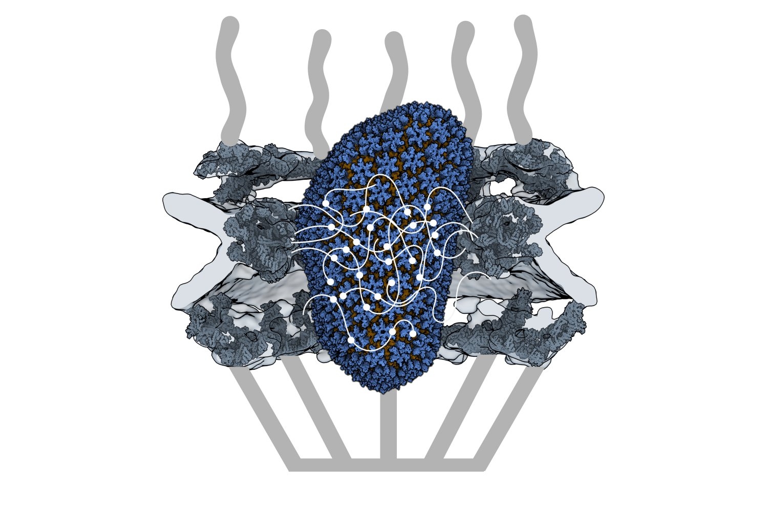
This optical micrograph shows an array of microscopic metamaterial samples on a reflective substrate. Laser pulses have been digitally added, depicting pump (red) and probe (green) pulses diagnosing a sample in the center. The LIRAS technique sweeps through all samples on the substrate within minutes.

MIT physicists turn pencil lead into “gold”

MIT physicists have metaphorically turned graphite, or pencil lead, into gold by isolating five ultrathin flakes stacked in a specific order. The resulting material can then be tuned to exhibit three important properties never before seen in natural graphite.

“It is kind of like one-stop shopping,” says Long Ju, an assistant professor in the Department of Physics and leader of the work, which is reported in the Oct. 5 issue of Nature Nanotechnology. “Nature has plenty of surprises. In this case, we never realized that all of these interesting things are embedded in graphite.”

Further, he says, “It is very rare material to find materials that can host this many properties.”

Graphite is composed of graphene, which is a single layer of carbon atoms arranged in hexagons resembling a honeycomb structure. Graphene, in turn, has been the focus of intense research since it was first isolated about 20 years ago. More recently, about five years ago, researchers including a team at MIT discovered that stacking individual sheets of graphene, and twisting them at a slight angle to each other, can impart new properties to the material, from superconductivity to magnetism. The field of “twistronics” was born.

In the current work, “we discovered interesting properties with no twisting at all,” says Ju, who is also affiliated with the Materials Research Laboratory.

He and colleagues discovered that five layers of graphene arranged in a certain order allow the electrons moving around inside the material to talk with each other. That phenomenon, known as electron correlation, “is the magic that makes all of these new properties possible,” Ju says.

Bulk graphite — and even single sheets of graphene — are good electrical conductors, but that’s it. The material Ju and colleagues isolated, which they call pentalayer rhombohedral stacked graphene, becomes much more than the sum of its parts.

Novel microscope

Key to isolating the material was a novel microscope Ju built at MIT in 2021 that can quickly and relatively inexpensively determine a variety of important characteristics of a material at the nanoscale. Pentalayer rhombohedral stacked graphene is only a few billionths of a meter thick.

Scientists including Ju were looking for multilayer graphene that was stacked in a very precise order, known as rhombohedral stacking. Says Ju, “there are more than 10 possible stacking orders when you go to five layers. Rhombohedral is just one of them.” The microscope Ju built, known as Scattering-type Scanning Nearfield Optical Microscopy, or s-SNOM, allowed the scientists to identify and isolate only the pentalayers in the rhombohedral stacking order they were interested in.

Three in one

From there, the team attached electrodes to a tiny sandwich composed of boron nitride “bread” that protects the delicate “meat” of pentalayer rhombohedral stacked graphene. The electrodes allowed them to tune the system with different voltages, or amounts of electricity. The result: They discovered the emergence of three different phenomena depending on the number of electrons flooding the system.

“We found that the material could be insulating, magnetic, or topological,” Ju says. The latter is somewhat related to both conductors and insulators. Essentially, Ju explains, a topological material allows the unimpeded movement of electrons around the edges of a material, but not through the middle. The electrons are traveling in one direction along a “highway” at the edge of the material separated by a median that makes up the center of the material. So the edge of a topological material is a perfect conductor, while the center is an insulator.

“Our work establishes rhombohedral stacked multilayer graphene as a highly tunable platform to study these new possibilities of strongly correlated and topological physics,” Ju and his coauthors conclude in Nature Nanotechnology.

In addition to Ju, authors of the paper are Tonghang Han and Zhengguang Lu. Han is a graduate student in the Department of Physics; Lu is a postdoc in the Materials Research Laboratory. The two are co-first authors of the paper.

Other authors are Giovanni Scuri, Jiho Sung, Jue Wang and Hongkun Park of Harvard University; Kenji Watanabe and Takashi Taniguchi of the National Institute for Materials Science in Japan; and Tianyi Han of the MIT Department of Physics.

This work was supported by a Sloan Fellowship; the U.S. National Science Foundation; the U.S. Office of the Under Secretary of Defense for Research and Engineering; the Japan Society for the Promotion of Science KAKENHI;  the World Premier International Research Initiative of Japan; and the U.S. Air Force Office of Scientific Research.

© Image: Sampson Wilcox/Research Laboratory of Electronics

Artist’s rendition of an electron correlation, or ability of electrons to talk with each other, that can occur in a special kind of graphite.

Using AI to optimize for rapid neural imaging

Connectomics, the ambitious field of study that seeks to map the intricate network of animal brains, is undergoing a growth spurt. Within the span of a decade, it has journeyed from its nascent stages to a discipline that is poised to (hopefully) unlock the enigmas of cognition and the physical underpinning of neuropathologies such as in Alzheimer’s disease. 

At its forefront is the use of powerful electron microscopes, which researchers from the MIT Computer Science and Artificial Intelligence Laboratory (CSAIL) and the Samuel and Lichtman Labs of Harvard University bestowed with the analytical prowess of machine learning. Unlike traditional electron microscopy, the integrated AI serves as a “brain” that learns a specimen while acquiring the images, and intelligently focuses on the relevant pixels at nanoscale resolution similar to how animals inspect their worlds. 

SmartEM” assists connectomics in quickly examining and reconstructing the brain’s complex network of synapses and neurons with nanometer precision. Unlike traditional electron microscopy, its integrated AI opens new doors to understand the brain's intricate architecture.

The integration of hardware and software in the process is crucial. The team embedded a GPU into the support computer connected to their microscope. This enabled running machine-learning models on the images, helping the microscope beam be directed to areas deemed interesting by the AI. “This lets the microscope dwell longer in areas that are harder to understand until it captures what it needs,” says MIT professor and CSAIL principal investigator Nir Shavit. “This step helps in mirroring human eye control, enabling rapid understanding of the images.” 

“When we look at a human face, our eyes swiftly navigate to the focal points that deliver vital cues for effective communication and comprehension,” says the lead architect of SmartEM, Yaron Meirovitch, a visiting scientist at MIT CSAIL who is also a former postdoc and current research associate neuroscientist at Harvard. “When we immerse ourselves in a book, we don't scan all of the empty space; rather, we direct our gaze towards the words and characters with ambiguity relative to our sentence expectations. This phenomenon within the human visual system has paved the way for the birth of the novel microscope concept.” 

For the task of reconstructing a human brain segment of about 100,000 neurons, achieving this with a conventional microscope would necessitate a decade of continuous imaging and a prohibitive budget. However, with SmartEM, by investing in four of these innovative microscopes at less than $1 million each, the task could be completed in a mere three months.

Nobel Prizes and little worms  

Over a century ago, Spanish neuroscientist Santiago Ramón y Cajal was heralded as being the first to characterize the structure of the nervous system. Employing the rudimentary light microscopes of his time, he embarked on leading explorations into neuroscience, laying the foundational understanding of neurons and sketching the initial outlines of this expansive and uncharted realm — a feat that earned him a Nobel Prize. He noted, on the topics of inspiration and discovery, that “As long as our brain is a mystery, the universe, the reflection of the structure of the brain will also be a mystery.”

Progressing from these early stages, the field has advanced dramatically, evidenced by efforts in the 1980s, mapping the relatively simpler connectome of C. elegans, small worms, to today’s endeavors probing into more intricate brains of organisms like zebrafish and mice. This evolution reflects not only enormous strides, but also escalating complexities and demands: mapping the mouse brain alone means managing a staggering thousand petabytes of data, a task that vastly eclipses the storage capabilities of any university, the team says. 

Testing the waters

For their own work, Meirovitch and others from the research team studied 30-nanometer thick slices of octopus tissue that were mounted on tapes, put on wafers, and finally inserted into the electron microscopes. Each section of an octopus brain, comprising billions of pixels, was imaged, letting the scientists reconstruct the slices into a three-dimensional cube at nanometer resolution. This provided an ultra-detailed view of synapses. The chief aim? To colorize these images, identify each neuron, and understand their interrelationships, thereby creating a detailed map or “connectome” of the brain's circuitry.

“SmartEM will cut the imaging time of such projects from two weeks to 1.5 days,” says Meirovitch. “Neuroscience labs that currently can't be engaged with expensive and long EM imaging will be able to do it now,” The method should also allow synapse-level circuit analysis in samples from patients with psychiatric and neurologic disorders. 

Down the line, the team envisions a future where connectomics is both affordable and accessible. They hope that with tools like SmartEM, a wider spectrum of research institutions could contribute to neuroscience without relying on large partnerships, and that the method will soon be a standard pipeline in cases where biopsies from living patients are available. Additionally, they’re eager to apply the tech to understand pathologies, extending utility beyond just connectomics. “We are now endeavoring to introduce this to hospitals for large biopsies, utilizing electron microscopes, aiming to make pathology studies more efficient,” says Shavit. 

Two other authors on the paper have MIT CSAIL ties: lead author Lu Mi MCS ’19, PhD ’22, who is now a postdoc at the Allen Institute for Brain Science, and Shashata Sawmya, an MIT graduate student in the lab. The other lead authors are Core Francisco Park and Pavel Potocek, while Harvard professors Jeff Lichtman and Aravi Samuel are additional senior authors. Their research was supported by the NIH BRAIN Initiative and was presented at the 2023 International Conference on Machine Learning (ICML) Workshop on Computational Biology. The work was done in collaboration with scientists from Thermo Fisher Scientific.

© Left image: Yaron Meirovitch via the Stable Diffusion XL AI image generator and Alex Shipps via the Midjourney AI image generator. Right image: Daniel Berger and Meirovitch, edited by Alex Shipps/MIT CSAIL

MIT researchers invented a technology and software to take electron microscopy to the next level by seamlessly integrating real-time machine learning into the imaging process — “smart microscopy.”

In a surprising finding, light can make water evaporate without heat

Evaporation is happening all around us all the time, from the sweat cooling our bodies to the dew burning off in the morning sun. But science’s understanding of this ubiquitous process may have been missing a piece all this time.

In recent years, some researchers have been puzzled upon finding that water in their experiments, which was held in a sponge-like material known as a hydrogel, was evaporating at a higher rate than could be explained by the amount of heat, or thermal energy, that the water was receiving. And the excess has been significant — a doubling, or even a tripling or more, of the theoretical maximum rate.

After carrying out a series of new experiments and simulations, and reexamining some of the results from various groups that claimed to have exceeded the thermal limit, a team of researchers at MIT has reached a startling conclusion: Under certain conditions, at the interface where water meets air, light can directly bring about evaporation without the need for heat, and it actually does so even more efficiently than heat. In these experiments, the water was held in a hydrogel material, but the researchers suggest that the phenomenon may occur under other conditions as well.

The findings are published this week in a paper in PNAS, by MIT postdoc Yaodong Tu, professor of mechanical engineering Gang Chen, and four others.

The phenomenon might play a role in the formation and evolution of fog and clouds, and thus would be important to incorporate into climate models to improve their accuracy, the researchers say. And it might play an important part in many industrial processes such as solar-powered desalination of water, perhaps enabling alternatives to the step of converting sunlight to heat first.

The new findings come as a surprise because water itself does not absorb light to any significant degree. That’s why you can see clearly through many feet of clean water to the surface below. So, when the team initially began exploring the process of solar evaporation for desalination, they first put particles of a black, light-absorbing material in a container of water to help convert the sunlight to heat.

Then, the team came across the work of another group that had achieved an evaporation rate double the thermal limit — which is the highest possible amount of evaporation that can take place for a given input of heat, based on basic physical principles such as the conservation of energy. It was in these experiments that the water was bound up in a hydrogel. Although they were initially skeptical, Chen and Tu starting their own experiments with hydrogels, including a piece of the material from the other group. “We tested it under our solar simulator, and it worked,” confirming the unusually high evaporation rate, Chen says. “So, we believed them now.” Chen and Tu then began making and testing their own hydrogels.

They began to suspect that the excess evaporation was being caused by the light itself —that photons of light were actually knocking bundles of water molecules loose from the water’s surface. This effect would only take place right at the boundary layer between water and air, at the surface of the hydrogel material — and perhaps also on the sea surface or the surfaces of droplets in clouds or fog.

In the lab, they monitored the surface of a hydrogel, a JELL-O-like matrix consisting mostly of water bound by a sponge-like lattice of thin membranes. They measured its responses to simulated sunlight with precisely controlled wavelengths.

The researchers subjected the water surface to different colors of light in sequence and measured the evaporation rate. They did this by placing a container of water-laden hydrogel on a scale and directly measuring the amount of mass lost to evaporation, as well as monitoring the temperature above the hydrogel surface. The lights were shielded to prevent them from introducing extra heat. The researchers found that the effect varied with color and peaked at a particular wavelength of green light. Such a color dependence has no relation to heat, and so supports the idea that it is the light itself that is causing at least some of the evaporation.

Animation shows evaporating by white condensation on glass under green light.

The researchers tried to duplicate the observed evaporation rate with the same setup but using electricity to heat the material, and no light. Even though the thermal input was the same as in the other test, the amount of water that evaporated never exceeded the thermal limit. However, it did so when the simulated sunlight was on, confirming that light was the cause of the extra evaporation.

Though water itself does not absorb much light, and neither does the hydrogel material itself, when the two combine they become strong absorbers, Chen says. That allows the material to harness the energy of the solar photons efficiently and exceed the thermal limit, without the need for any dark dyes for absorption.

Having discovered this effect, which they have dubbed the photomolecular effect, the researchers are now working on how to apply it to real-world needs. They have a grant from MIT’s Abdul Latif Jameel Water and Food Systems Lab to study the use of this phenomenon to improve the efficiency of solar-powered desalination systems, and a Bose Grant to explore the phenomenon’s effects on climate change modeling.

Tu explains that in standard desalination processes, “it normally has two steps: First we evaporate the water into vapor, and then we need to condense the vapor to liquify it into fresh water.” With this discovery, he says, potentially “we can achieve high efficiency on the evaporation side.” The process also could turn out to have applications in processes that require drying a material.

Chen says that in principle, he thinks it may be possible to increase the limit of water produced by solar desalination, which is currently 1.5 kilograms per square meter, by as much as three- or fourfold using this light-based approach. “This could potentially really lead to cheap desalination,” he says.

Tu adds that this phenomenon could potentially also be leveraged in evaporative cooling processes, using the phase change to provide a highly efficient solar cooling system.

Meanwhile, the researchers are also working closely with other groups who are attempting to replicate the findings, hoping to overcome skepticism that has faced the unexpected findings and the hypothesis being advanced to explain them.

The research team also included Jiawei Zhou, Shaoting Lin, Mohammed Alshrah, and Xuanhe Zhao, all in MIT’s Department of Mechanical Engineering.

© Image: iStock

At the interface of water and air, light can, in certain conditions, bring about evaporation without the need for heat, according to an MIT study.

From a five-layer graphene sandwich, a rare electronic state emerges

Ordinary pencil lead holds extraordinary properties when shaved down to layers as thin as an atom. A single, atom-thin sheet of graphite, known as graphene, is just a tiny fraction of the width of a human hair. Under a microscope, the material resembles a chicken-wire of carbon atoms linked in a hexagonal lattice.

Despite its waif-like proportions, scientists have found over the years that graphene is exceptionally strong. And when the material is stacked and twisted in specific contortions, it can take on surprising electronic behavior.

Now, MIT physicists have discovered another surprising property in graphene: When stacked in five layers, in a rhombohedral pattern, graphene takes on a very rare, “multiferroic” state, in which the material exhibits both unconventional magnetism and an exotic type of electronic behavior, which the team has coined ferro-valleytricity.

“Graphene is a fascinating material,” says team leader Long Ju, assistant professor of physics at MIT. “Every layer you add gives you essentially a new material. And now this is the first time we see ferro-valleytricity, and unconventional magnetism, in five layers of graphene. But we don’t see this property in one, two, three, or four layers.”

The discovery could help engineers design ultra-low-power, high-capacity data storage devices for classical and quantum computers.

“Having multiferroic properties in one material means that, if it could save energy and time to write a magnetic hard drive, you could also store double the amount of information compared to conventional devices,” Ju says.

His team reports their discovery today in Nature. MIT co-authors include lead author Tonghang Han, plus Zhengguang Lu, Tianyi Han, and Liang Fu; along with Harvard University collaborators Giovanni Scuri, Jiho Sung, Jue Wang, and Hongkun Park; and Kenji Watanabe and Takashi Taniguchi of the National Institute for Materials Science in Japan.

A preference for order

A ferroic material is one that displays some coordinated behavior in its electric, magnetic, or structural properties. A magnet is a common example of a ferroic material: Its electrons can coordinate to spin in the same direction without an external magnetic field. As a result, the magnet points to a preferred direction in space, spontaneously.

Other materials can be ferroic through different means. But only a handful have been found to be multiferroic — a rare state in which multiple properties can coordinate to exhibit multiple preferred states. In conventional multiferroics, it would be as if, in addition to the magnet pointing toward one direction, the electric charge also shifts in a direction that is independent from the magnetic direction.  

Multiferroic materials are of interest for electronics because they could potentially increase the speed and lower the energy cost of hard drives. Magnetic hard drives store data in the form of magnetic domains — essentially, microscopic magnets that are read as either a 1 or a 0, depending on their magnetic orientation. The magnets are switched by an electric current, which consumes a lot of energy and cannot operate quickly. If a storage device could be made with multiferroic materials, the domains could be switched by a faster, much lower-power electric field. Ju and his colleagues were curious about whether multiferroic behavior would emerge in graphene. The material’s extremely thin structure is a unique environment in which researchers have discovered otherwise hidden, quantum interactions. In particular, Ju wondered whether graphene would display multiferroic, coordinated behavior among its electrons when arranged under certain conditions and configurations.

“We are looking for environments where electrons are slowed down — where their interactions with the surrounding lattice of atoms is small, so that their interactions with other electrons can come through,” Ju explains. “That’s when we have some chance of seeing interesting collective behaviors of electrons.”

The team carried out some simple calculations and found that some coordinated behavior among electrons should emerge in a structure of five graphene layers stacked together in a rhombohedral pattern. (Think of five chicken-wire fences, stacked and slightly shifted such that, viewed from the top, the structure would resemble a pattern of diamonds.)

“In five layers, electrons happen to be in a lattice environment where they move very slowly, so they can interact with other electrons effectively,” Ju says. “That’s when electron correlation effects start to dominate, and they can start to coordinate into certain preferred, ferroic orders.”

Magic flakes

The researchers then went into the lab to see whether they could actually observe multiferroic behavior in five-layer graphene. In their experiments, they started with a small block of graphite, from which they carefully exfoliated individual flakes. They used optical techniques to examine each flake, looking specifically for five-layer flakes, arranged naturally in a rhombohedral pattern.

“To some extent, nature does the magic,” said lead author and graduate student Han. “And we can look at all these flakes and tell which has five layers, in this rhombohedral stacking, which is what should give you this slowing-down effect in electrons.”

The team isolated several five-layer flakes and studied them at temperatures just above absolute zero. In such ultracold conditions, all other effects, such as thermally induced disorders within graphene, should be dampened, allowing interactions between electrons, to emerge. The researchers measured electrons’ response to an electric field and a magnetic field, and found that indeed, two ferroic orders, or sets of coordinated behaviors, emerged.

The first ferroic property was an unconventional magnetism: The electrons coordinated their orbital motion, like planets circling in the same direction. (In conventional magnets, electrons coordinate their “spin” — rotating in the same direction, while staying relatively fixed in space.)

The second ferroic property had to do with graphene’s electronic “valley.” In every conductive material, there are certain energy levels that electrons can occupy. A valley represents the lowest energy state that an electron can naturally settle. As it turns out, there are two possible valleys in graphene. Normally, electrons have no preference for either valley and settle equally into both.

But in five-layer graphene, the team found that the electrons began to coordinate, and preferred to settle in one valley over the other. This second coordinated behavior indicated a ferroic property that, combined with the electrons’ unconventional magnetism, gave the structure a rare, multiferroic state.

“We knew something interesting would happen in this structure, but we didn’t know exactly what, until we tested it,” says co-first author Lu, a postdoc in Ju’s group. “It’s the first time we’ve seen a ferro-valleytronics, and also the first time we’ve seen a coexistence of ferro-valleytronics with unconventional ferro-magnet.”

The team showed they could control both ferroic properties using an electric field. They envision that, if engineers can incorporate five-layer graphene or similar multiferroic materials into a memory chip, they could, in principle, use the same, low-power electric field to manipulate the material’s electrons in two ways rather than one, and effectively double the data that could be stored on a chip compared to conventional multiferroics. While that vision is far from practical realization, the team’s results break new ground in the search for better, more efficient electronic, magnetic and valleytronic devices.

This research was done, in part, using the electron-beam lithography facility run by MIT.nano, and is funded, in part, by the National Science Foundation and the Sloan Foundation.

© Image: Sampson Wilcox, RLE

When stacked in five layers in a rhombohedral pattern, graphene takes on a rare “multiferroic” state, in which the material’s electrons (illustrated here as spheres) exhibit two preferred electronic states: an unconventional magnetism (represented as orbits around each electron), and “valley,” or a preference for one of two energy states (depicted in red versus blue). The results could help advance more powerful magnetic memory devices.

Photos: Moungi Bawendi’s first day as a Nobel laureate

Today, MIT Professor Moungi Bawendi won a share of the 2023 Nobel Prize in Chemistry, for his role in developing quantum dots — nanoscale particles that can emit exceedingly bright light. Bawendi, a professor of chemistry who has been on the MIT faculty since 1990, told MIT News this morning that he felt “surprise and shock” upon receiving the call from the Nobel committee from his home in Cambridge, Massachusetts, adding, “It was such an honor to wake up to.”

The following images provide a brief snapshot of his first day as a Nobel laureate.

Photo of Moungi Bawendi smiling while seated on a couch with the text from @NobelPrize: “Say hello! Moungi Bawendi got an early morning call from Stockholm breaking the news that he is one of the 2023 chemistry laureates. How is he celebrating this morning? Teaching his MIT class at 9. We'll be sharing his first reaction very soon."

Early this morning, Bawendi received a phone call from Nobel Prize officials in Sweden, letting him know that he had won a share of this year’s chemistry prize. Hear some of his first reactions via a Nobel Prize phone interview.

Three people seated at a table in conference room, with the Nobel Prize in Chemistry winners projected on screen behind them

Bawendi took his first questions from the media during a 5:45 a.m. (ET) press conference hosted by the Royal Swedish Academy of Sciences in Stockholm to announce this year’s winners. Watch the full press conference.

Moungi Bawendi smiles while talking on his cell phone. A framed print of a large clock is in the background.

He quickly began to receive texts and calls from family, friends, colleagues, and more.

Moungi Bawendi sits on a sofa in his living room, looking at laptop in front of him on a coffee table and speaking into a cell phone. Family members are in the background; a large camera on a tripod is in the foreground.

Media crews soon arrived at his home in Cambridge, where his wife, Rachel Zimmerman; stepdaughter, Julia Teller; and very good dog Phoebe were celebrating with him.

Moungi Bawendi, casually dressed, stands on the steps outside his home. His dog Phoebe poses next to him, proud of her human.

The Nobel laureate joined Phoebe for official MIT portrait photos.

X post from Dane DeQuilettes with a video still of Moungi Bawendi popping champagne with more than a dozen others indoors. Text: Congrats Moungi! I know that the #NobelPrize doesn’t factor in teaching and mentorship, but he is someone that does it all. So many of us have benefited from his thoughtful skepticism, creative problem solving, and guidance throughout the years. Cheers!

Bawendi arrived at the MIT campus shortly before he was scheduled to teach, and was greeted with applause and festive food and drinks from his colleagues and students.

Moungi Bawendi talks and laughs with three other students and faculty member outside a classroom.

Following a sartorial update, Bawendi prepared to teach his 9 a.m. class, greeting more colleagues and students in the Department of Chemistry.

Moungi Bawendi stands at the front of a classroom facing several rows of MIT students.

Bawendi ended up scrapping plans for his class, 5.73 (Introduction to Quantum Mechanics), switching from a normal lesson to a brief history of his work on quantum dot science. The class “went very well, except I didn’t talk about what I was supposed to talk about,” he joked afterward, at an MIT press conference.

Moungi Bawendi poses with an MIT student. Another student in the foreground, with her back to the camera, holds out her phone to take the photo.

After class, the professor of chemistry made time to take photos with students.

A screenshot of Moungi Bawendi speaking in the online press conference. He is seated, with a table and chalkboard behind him. At the top of the screen is the title “MIT Nobel Prize Live Press Conference.”

An MIT press conference, hosted by the Institute Office of Communications and President Sally Kornbluth, was held at 10:30 a.m. ET. Watch the full press conference.

Sally Kornbluth and Moungai Bawendi stand facing each other in front of sign that says "Massachusetts Institute of Technology"

After lunch, Bawendi met in person with President Kornbluth.

Moungi Bawendi is surrounded by colleagues as they toast his achievement.

In the late afternoon, toasts were made at a celebration for Bawendi organized by the Department of Chemistry.

© Photo: Jodi Hilton

It was an early start for Moungi Bawendi and his wife, Rachel Zimmerman, as they celebrated his receipt of a Nobel Prize in Chemistry on Wednesday, Oct. 4.

MIT Professor Moungi Bawendi shares Nobel Prize in Chemistry

Moungi Bawendi, the Lester Wolfe Professor of Chemistry at MIT and a leader in the development of tiny particles known as quantum dots, has won the Nobel Prize in Chemistry for 2023. He will share the prize with Louis Brus of Columbia University and Alexei Ekimov of Nanocrystals Technology, Inc.

The researchers were honored for their work in discovering and synthesizing quantum dots — tiny particles of matter that emit exceptionally pure light. In its announcement this morning, the Nobel Foundation cited Bawendi for work that “revolutionized the chemical production of quantum dots, resulting in almost perfect particles.”

Bawendi, who has been a professor at MIT since 1990, told MIT News this morning that he felt “surprise and shock” upon receiving the call from the Nobel committee, adding, “It was such an honor to wake up to.”

Quantum dots consist of tiny particles of semiconductor material that are so small that their properties differ from those of the bulk material. Instead, they are governed in part by the laws of quantum mechanics that describe how atoms and subatomic particles behave. When illuminated with ultraviolet light, the dots fluoresce brightly in a range of colors determined by the sizes of the particles.

These tiny particles are now used in many types of biomedical imaging, as well as computer and television displays, and they also hold potential in fields such as photocatalysis and quantum computing.

“It’s hard to think of a more elegant expression of Mind and Hand,” MIT President Sally Kornbluth wrote about Bawendi’s work, in a letter to the MIT community this morning, in reference to MIT’s motto, “Mens et Manus.” “We join Moungi’s family, his department, and his friends and colleagues around the world in celebrating this rare honor.”

Sculpting tiny particles

Quantum dots are particles only a few nanometers in diameter — about one-millionth the size of a pinhead. Since the 1930s, scientists had predicted that particles so tiny would show unusual behavior because at such tiny scales there is less space for a material’s electrons, so they become squeezed together. As a result, it was believed that the particles’ size would influence physical properties such as color.

However, this hypothesis was difficult to test because there were no ways to produce such tiny particles — until the early 1980s, when Ekimov and Brus independently succeeded at creating quantum dots. Working with quantum dots floating freely in a solution, Brus demonstrated that the size of the particles affected the color that they emitted. Ekimov discovered the same phenomenon working with nanoparticles of glass tinted with copper chloride.

The techniques used by Ekimov and Brus, however, did not yield quantum dots of uniform size. In 1993, Bawendi and his students were the first to report a method for synthesizing quantum dots while maintaining precise control over their size.

By systematically varying the conditions under which the quantum dots were crystallized, Bawendi and his research group succeeded in growing nanocrystals of a specific size. At the time, the researchers were interested in making quantum dots so they could further study their unique properties, with no inkling of what they would later become useful for.

“We just pushed and pushed, and we eventually developed a process to make particles good enough for basic science studies, and it turned out the process could be used for far more than that, which we never would have thought at the time,” Bawendi told MIT News.

Since then, he has also devised ways to control the efficiency of the dots’ light emission and to eliminate their tendency to blink on and off, making them more practical for applications in many fields.

Quantum dots are now used in flat screen TVs and other displays, where they generate more vivid images than traditional LED screens. They are also used to label molecules inside cells, allowing them to be imaged more easily, and they have been explored as a tool to guide doctors during surgery by illuminating tissue.

“It’s really great to see how they have been used in so many areas, but it’s not something we were expecting at the time,” says Bawendi, who is also a core member of the Microsystems Technology Laboratories at MIT. “We were just interested in studying the materials.”

Introducing Bawendi at an MIT press conference this morning, Kornbluth described his Nobel achievement as “a banner day” for the Institute.

“We cannot imagine anything more electrifying,” Kornbluth said. “Obviously, that excitement reflects our respect for this extraordinary honor, but it runs deeper because you'd be hard pressed to find a community with a greater reverence for the wondrous beauty of basic discovery science and the incredible power of innovation to better our world than the people of MIT. I hope this award and all of this week's science Nobels can serve to remind the nation and the world of why fundamental science deserves our sustained and enthusiastic support.”

A new field of science

Born in Paris to a French mother and Tunisian father, Bawendi moved to West Lafayette, Indiana, as a young boy when his father, a mathematician, became a professor at Purdue University. In 1982, he earned his undergraduate degree from Harvard University, where as a first-year student, he failed his first chemistry exam. That experience taught him a valuable lesson in perseverance, which he described at today’s press conference.

“You have a setback, but you can persevere and overcome this and learn from your experience, which obviously I did,” he said. “And I could have just decided this wasn't for me, but I liked what I was doing, and so I learned how to become successful as a student.”

Bawendi went on to earn a PhD from the University of Chicago in 1988. As a postdoc, he worked with Brus, who was then at AT&T Bell Laboratories and had recently made his original discovery regarding the properties of different sized quantum dots.

“That was what made me excited to work with him, because it opened up a brand new field of science, which creates a lot of opportunity to make new discoveries,” Bawendi told MIT News.

Scientists are now exploring the possibility of using quantum dots to improve the performance of many other technologies, including solar cells, flexible electronics, and photocatalysts. In recent years, Bawendi’s lab has also developed spectrometers based on quantum dots, which are small enough to fit inside a smartphone camera. Such devices could be used to diagnose diseases, especially skin conditions, or to detect environmental pollutants.

When asked at the press conference what the future might hold for quantum dot research, Bawendi said he expects to be surprised.

“That's a really good question because I'm constantly surprised when I go to conferences about the progress and the directions of the field,” he said. “I think 30 years ago, none of us who started the field could have predicted 30 years later we’d be where we are today. And it's just amazing to me, if you have really great people working on a brand new field with brand new materials, innovation comes out in directions that you can't predict.”

Being at MIT, with its focus on interdisciplinary research, has been a critical factor in his success, Bawendi told MIT News.

“The atmosphere at MIT is really what allowed me to explore other fields of science, which has been key to the advances I’ve been able to make,” he says. “It’s a unique place, and it’s wonderful to be part of it.”

© Photo: Len Rubenstein

Moungi Bawendi

Quantum repeaters use defects in diamond to interconnect quantum systems

The popular children's game of telephone is based on a simple premise: The starting player whispers a message into the ear of the next player. That second player then passes along the message to the third person and so on until the message reaches the final recipient, who relays it to the group aloud. Often, what the first person said and the last person heard are laughably different; the information gets garbled along the chain.

Such transmission errors from start to end point are also common in the quantum world. As quantum information bits, or qubits (the analogs of classical bits in traditional digital electronics), make their way over a channel, their quantum states can degrade or be lost entirely. Such decoherence is especially common over longer and longer distances because qubits — whether existing as particles of light (photons), electrons, atoms, or other forms — are inherently fragile, governed by the laws of quantum physics, or the physics of very small objects. At this tiny scale (nanoscale), even slight interactions with their environment can cause qubits to lose their quantum properties and alter the information they store. Like the game of telephone, the original and received messages may not be the same.

"One of the big challenges in quantum networking is how to effectively move these delicate quantum states between multiple quantum systems," says Scott Hamilton, leader of MIT Lincoln Laboratory's Optical and Quantum Communications Technology Group, part of the Communications Systems R&D area. "That's a question we're actively exploring in our group."

As Hamilton explains, today's quantum computing chips contain on the order of 100 qubits. But thousands, if not billions, of qubits are required to make a fully functioning quantum computer, which promises to unlock unprecedented computational power for applications ranging from artificial intelligence and cybersecurity to health care and manufacturing. Interconnecting the chips to make one big computer may provide a viable path forward. On the sensing front, connecting quantum sensors to share quantum information may enable new capabilities and performance gains beyond those of an individual sensor. For example, a shared quantum reference between multiple sensors could be used to more precisely locate radio-frequency emission sources. Space and defense agencies are also interested in interconnecting quantum sensors separated by long ranges for satellite-based position, navigation, and timing systems or atomic clock networks between satellites. For communications, quantum satellites could be used as part of a quantum network architecture connecting local ground-based stations, creating a truly global quantum internet.

However, quantum systems can't be interconnected with existing technology. The communication systems used today to transmit information across a network and connect devices rely on detectors that measure bits and amplifiers that copy bits. These technologies do not work in a quantum network because qubits cannot be measured or copied without destroying the quantum state; qubits exist in a superposition of states between zero and one, as opposed to classical bits, which are in a set state of either zero (off) or one (on). Therefore, researchers have been trying to develop the quantum equivalents of classical amplifiers to overcome transmission and interconnection loss. These equivalents are known as quantum repeaters, and they work similarly in concept to amplifiers, dividing the transmission distance into smaller, more manageable segments to lessen losses.

"Quantum repeaters are a critical technology for quantum networks to successfully send information over lossy links," Hamilton says. "But nobody has made a fully functional quantum repeater yet."

The complexity lies in how quantum repeaters operate. Rather than employing a simple "copy and paste," as classical repeaters do, quantum repeaters work by leveraging a strange quantum phenomenon called entanglement. In quantum entanglement, two particles become strongly connected and correlated across space, no matter the distance between them. If you know the state of one particle in an entangled pair, then you automatically know the state of the other. Entangled qubits can serve as a resource for quantum teleportation, in which quantum information is sent between distant systems without moving actual particles; the information vanishes at one location and reappears at another. Teleportation skips the physical journey along fiber-optic cables and therefore eliminates the associated risk of information loss. Quantum repeaters are what tie everything together: they enable the end-to-end generation of quantum entanglement, and, ultimately, with quantum teleportation, the end-to-end transmission of qubits.

Ben Dixon, a researcher in the Optical and Quantum Communications Technology Group, explains how the process works: "First, you need to generate pairs of specific entangled qubits (called Bell states) and transmit them in different directions across the network link to two separate quantum repeaters, which capture and store these qubits. One of the quantum repeaters then does a two-qubit measurement between the transmitted and stored qubit and an arbitrary qubit that we want to send across the link in order to interconnect the remote quantum systems. The measurement results are communicated to the quantum repeater at the other end of the link; the repeater uses these results to turn the stored Bell state qubit into the arbitrary qubit. Lastly, the repeater can send the arbitrary qubit into the quantum system, thereby linking the two remote quantum systems."

To retain the entangled states, the quantum repeater needs a way to store them — in essence, a memory. In 2020, collaborators at Harvard University demonstrated holding a qubit in a single silicon atom (trapped between two empty spaces left behind by removing two carbon atoms) in diamond. This silicon "vacancy" center in diamond is an attractive quantum memory option. Like other individual electrons, the outermost (valence) electron on the silicon atom can point either up or down, similar to a bar magnet with north and south poles. The direction that the electron points is known as its spin, and the two possible spin states, spin up or spin down, are akin to the ones and zeros used by computers to represent, process, and store information. Moreover, silicon's valence electron can be manipulated with visible light to transfer and store a photonic qubit in the electron spin state. The Harvard researchers did exactly this; they patterned an optical waveguide (a structure that guides light in a desired direction) surrounded by a nanophotonic optical cavity to have a photon strongly interact with the silicon atom and impart its quantum state onto that atom. Collaborators at MIT then showed this basic functionality could work with multiple waveguides; they patterned eight waveguides and successfully generated silicon vacancies inside them all. 

Lincoln Laboratory has since been applying quantum engineering to create a quantum memory module equipped with additional capabilities to operate as a quantum repeater. This engineering effort includes on-site custom diamond growth (with the Quantum Information and Integrated Nanosystems Group); the development of a scalable silicon-nanophotonics interposer (a chip that merges photonic and electronic functionalities) to control the silicon-vacancy qubit; and integration and packaging of the components into a system that can be cooled to the cryogenic temperatures needed for long-term memory storage. The current system has two memory modules, each capable of holding eight optical qubits.

To test the technologies, the team has been leveraging an optical-fiber test bed leased by the laboratory. This test bed features a 50-kilometer-long telecommunications network fiber currently connecting three nodes: Lincoln Laboratory to MIT campus and MIT campus to Harvard. Local industrial partners can also tap into this fiber as part of the Boston-Area Quantum Network (BARQNET).

"Our goal is to take state-of-the-art research done by our academic partners and transform it into something we can bring outside the lab to test over real channels with real loss," Hamilton says. "All of this infrastructure is critical for doing baseline experiments to get entanglement onto a fiber system and move it between various parties."

Using this test bed, the team, in collaboration with MIT and Harvard researchers, became the first in the world to demonstrate a quantum interaction with a nanophotonic quantum memory across a deployed telecommunications fiber. With the quantum repeater located at Harvard, they sent photons encoded with quantum states from the laboratory, across the fiber, and interfaced them with the silicon-vacancy quantum memory that captured and stored the transmitted quantum states. They measured the electron on the silicon atom to determine how well the quantum states were transferred to the silicon atom's spin-up or spin-down position.

"We looked at our test bed performance for the relevant quantum repeater metrics of distance, efficiency (loss error), fidelity, and scalability and found that we achieved best or near-best for all these metrics, compared to other leading efforts around the world," Dixon says. "Our distance is longer than anybody else has shown; our efficiency is decent, and we think we can further improve it by optimizing some of our test bed components; the read-out qubit from memory matches the qubit we sent with 87.5 percent fidelity; and diamond has an inherent lithographic patterning scalability in which you can imagine putting thousands of qubits onto one small chip." 

The Lincoln Laboratory team is now focusing on combining multiple quantum memories at each node and incorporating additional nodes into the quantum network test bed. Such advances will enable the team to explore quantum networking protocols at a system level. They also look forward to materials science investigations that their Harvard and MIT collaborators are pursuing. These investigations may identify other types of atoms in diamond capable of operating at slightly warmer temperatures for more practical operation.

The nanophotonic quantum memory module was recognized with a 2023 R&D 100 Award.

© Photo: Glen Cooper

A packaged prototype quantum repeater module (center), mounted on a gold-plated copper assembly and connected to printed circuit boards (green), features eight optical memories that store qubits in a silicon atom in diamond.

MIT.nano Family Day invites those at home to come to work

Every day, researchers come to MIT.nano to investigate at the nanoscale, but what’s it like to work there? On Aug. 21, MIT.nano staff invited their family members to come see what it takes to support discovery, education, and innovation in this cutting-edge research facility.

More than 50 people attended — spouses and partners, parents and children, nephews and nieces, in-laws, and others. The event was so much fun that staff and families alike were asking to do it again; by the end of the day calling it the “first annual” MIT.nano Family Day.

After a welcome from Vladimir Bulović, faculty director of MIT.nano and Fariborz Maseeh Professor of Emerging Technologies, technical staff introduced the families to the building and its various facilities. Following a behind-the-scenes tour of some of the infrastructure spaces, they enjoyed lunch in MIT.nano’s East Lobby, then split into groups for hands-on experiences throughout the building.

In MIT.nano’s characterization facility, visitors gained a firsthand look at the powerful microscopes positioned inside the basement imaging suites and learned how to minimize vibrational and electromagnetic interference in order to make videos of atoms. In one suite, the guests viewed individual columns of atoms using an aberration-corrected scanning transmission electron microscope. In another, staff demonstrated how to use micro-computed tomography (microCT) to obtain three-dimensional imagery of the interior of electronic devices, biological samples, and other objects.

The next stop was the MIT.nano Immersion Lab for demonstrations of sensing technology and immersive experiences. Family members put on a mixed-reality headset and were transported — virtually — into the cockpit of an airplane preparing for takeoff. Those not interested in flying stepped inside a virtual art studio complete with balloons on the ceiling and snow falling outside.

Family members also donned full-body protective clothing called “bunny suits” and headed into MIT.nano’s cleanroom. As they toured the nanofabrication facility, the visitors observed researchers operating equipment and tested a particle counter that illustrated just how much of a wrecking ball dust can be at the nanoscale. A smaller group of volunteers joined MIT.nano staff in using the cleanroom processing tools to expose, develop, and etch a Family Day group photo onto a 50-nanometer-thick layer of aluminum on a silicon wafer, now displayed in MIT.nano’s first floor cleanroom window.

The day concluded with an ice cream social and swag grab in MIT.nano’s courtyard, where staff and their visitors mingled with one another as a new, extended MIT and MIT.nano family.

© Photo collage: Tom Gearty

MIT.nano Family Day brought over 50 family members of MIT.nano staff to MIT for a fun-filled day of nanoscale exploration.

Pixel-by-pixel analysis yields insights into lithium-ion batteries

By mining data from X-ray images, researchers at MIT, Stanford University, SLAC National Accelerator, and the Toyota Research Institute have made significant new discoveries about the reactivity of lithium iron phosphate, a material used in batteries for electric cars and in other rechargeable batteries.

The new technique has revealed several phenomena that were previously impossible to see, including variations in the rate of lithium intercalation reactions in different regions of a lithium iron phosphate nanoparticle.

The paper’s most significant practical finding — that these variations in reaction rate are correlated with differences in the thickness of the carbon coating on the surface of the particles — could lead to improvements in the efficiency of charging and discharging such batteries.

“What we learned from this study is that it’s the interfaces that really control the dynamics of the battery, especially in today’s modern batteries made from nanoparticles of the active material. That means that our focus should really be on engineering that interface,” says Martin Bazant, the E.G. Roos Professor of Chemical Engineering and a professor of mathematics at MIT, who is the senior author of the study.

63 pairs of almond-shaped iron phosphate particles colored red, green, and yellow are pictured upon black background. Each pair has a pointer below with green center that stays still as the red end spins clockwise.

This approach to discovering the physics behind complex patterns in images could also be used to gain insights into many other materials, not only other types of batteries but also biological systems, such as dividing cells in a developing embryo.

“What I find most exciting about this work is the ability to take images of a system that’s undergoing the formation of some pattern, and learning the principles that govern that,” Bazant says.

Hongbo Zhao PhD ’21, a former MIT graduate student who is now a postdoc at Princeton University, is the lead author of the new study, which appears today in Nature. Other authors include Richard Bratz, the Edwin R. Gilliland Professor of Chemical Engineering at MIT; William Chueh, an associate professor of materials science and engineering at Stanford and director of the SLAC-Stanford Battery Center; and Brian Storey, senior director of Energy and Materials at the Toyota Research Institute.

“Until now, we could make these beautiful X-ray movies of battery nanoparticles at work, but it was challenging to measure and understand subtle details of how they function because the movies were so information-rich,” Chueh says. “By applying image learning to these nanoscale movies, we can extract insights that were not previously possible.”

Modeling reaction rates

Lithium iron phosphate battery electrodes are made of many tiny particles of lithium iron phosphate, surrounded by an electrolyte solution. A typical particle is about 1 micron in diameter and about 100 nanometers thick. When the battery discharges, lithium ions flow from the electrolyte solution into the material by an electrochemical reaction known as ion intercalation. When the battery charges, the intercalation reaction is reversed, and ions flow in the opposite direction.

“Lithium iron phosphate (LFP) is an important battery material due to low cost, a good safety record, and its use of abundant elements,” Storey says. “We are seeing an increased use of LFP in the EV market, so the timing of this study could not be better.”

Before the current study, Bazant had done a great deal of theoretical modeling of patterns formed by lithium-ion intercalation. Lithium iron phosphate prefers to exist in one of two stable phases: either full of lithium ions or empty. Since 2005, Bazant has been working on mathematical models of this phenomenon, known as phase separation, which generates distinctive patterns of lithium-ion flow driven by intercalation reactions. In 2015, while on sabbatical at Stanford, he began working with Chueh to try to interpret images of lithium iron phosphate particles from scanning transmission X-ray microscopy.

Using this type of microscopy, the researchers can obtain images that reveal the concentration of lithium ions, pixel-by-pixel, at every point in the particle. They can scan the particles several times as the particles charge or discharge, allowing them to create movies of how lithium ions flow in and out of the particles.

In 2017, Bazant and his colleagues at SLAC received funding from the Toyota Research Institute to pursue further studies using this approach, along with other battery-related research projects.

By analyzing X-ray images of 63 lithium iron phosphate particles as they charged and discharged, the researchers found that the movement of lithium ions within the material could be nearly identical to the computer simulations that Bazant had created earlier. Using all 180,000 pixels as measurements, the researchers trained the computational model to produce equations that accurately describe the nonequilibrium thermodynamics and reaction kinetics of the battery material.

“Every little pixel in there is jumping from full to empty, full to empty. And we’re mapping that whole process, using our equations to understand how that’s happening,” Bazant says.

The researchers also found that the patterns of lithium-ion flow that they observed could reveal spatial variations in the rate at which lithium ions are absorbed at each location on the particle surface.

“It was a real surprise to us that we could learn the heterogeneities in the system — in this case, the variations in surface reaction rate — simply by looking at the images,” Bazant says. “There are regions that seem to be fast and others that seem to be slow.”

Furthermore, the researchers showed that these differences in reaction rate were correlated with the thickness of the carbon coating on the surface of the lithium iron phosphate particles. That carbon coating is applied to lithium iron phosphate to help it conduct electricity — otherwise the material would conduct too slowly to be useful as a battery.

“We discovered at the nano scale that variation of the carbon coating thickness directly controls the rate, which is something you could never figure out if you didn't have all of this modeling and image analysis,” Bazant says.

The findings also offer quantitative support for a hypothesis Bazant formulated several years ago: that the performance of lithium iron phosphate electrodes is limited primarily by the rate of coupled ion-electron transfer at the interface between the solid particle and the carbon coating, rather than the rate of lithium-ion diffusion in the solid.

Optimized materials

The results from this study suggest that optimizing the thickness of the carbon layer on the electrode surface could help researchers to design batteries that would work more efficiently, the researchers say.

“This is the first study that's been able to directly attribute a property of the battery material with a physical property of the coating,” Bazant says. “The focus for optimizing and designing batteries should be on controlling reaction kinetics at the interface of the electrolyte and electrode.”

“This publication is the culmination of six years of dedication and collaboration,” Storey says. “This technique allows us to unlock the inner workings of the battery in a way not previously possible. Our next goal is to improve battery design by applying this new understanding.”  

In addition to using this type of analysis on other battery materials, Bazant anticipates that it could be useful for studying pattern formation in other chemical and biological systems.

This work was supported by the Toyota Research Institute through the Accelerated Materials Design and Discovery program.

© Courtesy of the researchers

By mining X-ray images, MIT researchers have made significant new discoveries about the reactivity of lithium iron phosphate, a material used in batteries for electric cars and in other rechargeable batteries. In each pair pictured, actual particles are on the left and the researchers’ simulations are on the right.

Internships fabricate a microelectronics future

Nestled among the diverse labs and prototyping facilities at MIT Lincoln Laboratory, the Microelectronics Laboratory (ML) whirs away. Technicians in the ML fabricate advanced integrated circuits, which end up in systems that peer into the cosmos, observe weather from space, and power quantum computers — to name just a few uses. The ML is one of several facilities within Lincoln Laboratory’s Microsystems Prototyping Foundry (MPF) operations.

This summer, 12 students had a hand in MPF operations as part of the Massachusetts Microelectronics Internship Program. The Northeast Microelectronics Coalition started this program last year to help train the next generation of microelectronics professionals. Accepted undergraduates are placed in the region's leading microelectronics companies for 10 weeks. No prior experience is needed, only a willingness to learn.

Donning "bunny suits," the head-to-toe coverings staff wear to help keep the lab free from contaminants, the interns each conducted experiments to improve fabrication processes. The ML maintains an ultraclean certification, Class 10/ISO 4, meaning that the air contains a maximum of 10 particles (over 0.5 micron in size) per cubic foot. Even so, particles can still end up on the wafers — slices of semiconductor materials, like silicon, that form the base of circuits.

"Particles can be device killers. Cleanrooms control and reduce the amount and size of particles," says Peter Preston, an intern from Springfield Technical Community College (STCC). Over the summer, Preston assessed the number of particles present on wafers after they underwent specific processing steps and troubleshooted ways to lower that count. Fellow STCC student Travis Donelon sampled the ML's water supply to test for bacteria, which can introduce particles to the water during rinsing. He also analyzed the flow of nitrogen gas, an essential material for keeping surfaces free of moisture and particles throughout every step of the fabrication process.

In running these experiments, Preston and Donelon learned how to run each machine in the Compound Semiconductor Laboratory (CSL) within the MPF, training that could enable them to be “hired tomorrow as technicians," says Scott Eastwood, the CSL operations manager.

"Getting hands-on work with almost every tool used in the fabrication process was a great opportunity to see the big picture of what microelectronics is all about," Donelon says.

Dan Pulver, the ML group leader, says that the internships are helping the ML plot a route of growth. "We’re building skills and opportunity awareness, along with relationships, with more students who may go on to work in our group." A recent self-assessment showed that the ML has the most retirement risk of all groups at Lincoln Laboratory — a finding that mirrors the microelectronics workforce, both regionally and nationally. 

Experts find that the industry's knowledge base is shrinking fast, as U.S. dominance in semiconductors has receded in recent decades. A chip shortage during the Covid-19 pandemic shone a light on the risks of relying on overseas microelectronics fabrication. The 2022 CHIPS (for Creating Helpful Incentives to Produce Semiconductors) and Science Act aims to ramp-up chip fabrication and innovation in the United States, but a new generation of workers will need the relevant knowledge to do so. This internship program was made possible, in part, by funding from CHIPS, which allocated $13.2 billion for R&D and workforce development.

Kara Stratton, a rising junior at Boston University, credits this internship with her decision to now pursue a nanotechnology concentration. Her summer project involved teasing out issues in the process of depositing platinum. In creating circuits, platinum (among other metals) is heated in a low-pressure chamber, vaporized, and deposited onto a wafer. She made changes to the platinum recipe and heat-up processes to reduce spitting, or uneven deposits.

"Having a hands-on job that taught me so much and gave me priceless experiences made me feel more confident in making the decision to pursue a career in microelectronics," Stratton says. "Lincoln Laboratory, and more specifically the ML, fosters an inclusive and innovative community of employees who were always willing to help me learn new things."

Some students will continue their work in the fall as student technical assistants. "We often see the eyes of students light up as they discuss new experiences and accomplishments — a great short-term reward. I think long term will work out, too," Pulver says. One student, Ian Pahl from Western New England University, hopes to progress his research in reducing ML energy use. One of his projects studied the impact of reducing airflow fan speeds, a change that could save the ML up to $100,000 a year along with carbon footprint reduction, according to Pulver.

Besides the time spent in the ML, each intern also gained mentorship, participated in training events, and learned more about the diverse projects undertaken at a federally funded R&D center. They received subsidized housing and transportation, as part of the many benefits Lincoln Laboratory offers through its wider Summer Research Program.

As Donelon heads back to school to study optics and photonics, he looks forward to expanding on his newfound knowledge. "My internship experience was nothing short of incredible. Coming from a switched major and community college, I was not expecting but very humbled to be working at such a prestigious laboratory. The work I have done over the summer has been both challenging and gratifying."

Students interested in applying for the Massachusetts Microelectronics Internship Program can learn more on the program’s website.

© Photo: Nicole Fandel

Students enrolled in the Massachusetts Microelectronics Internship Program gained experience with Lincoln Laboratory’s Microsystems Prototyping Foundry operations this summer.

MIT engineers design more powerful RNA vaccines

RNA vaccines against Covid-19 have proven effective at reducing the severity of disease. However, a team of researchers at MIT is working on making them even better. By tweaking the design of the vaccines, the researchers showed that they could generate Covid-19 RNA vaccines that produce a stronger immune response, at a lower dose, in mice.

Adjuvants are molecules commonly used to increase the immune response to vaccines, but they haven’t yet been used in RNA vaccines.  In this study, the MIT researchers engineered both the nanoparticles used to deliver the Covid-19 antigen, and the antigen itself, to boost the immune response, without the need for a separate adjuvant.

If further developed for use in humans, this type of RNA vaccine could help to reduce costs, reduce the dosage needed, and potentially lead to longer-lasting immunity. The researchers’ tests also showed that when delivered intranasally, the vaccine induced a strong immune response when compared to the response elicited by traditional, intramuscular vaccination.

“With intranasal vaccination, you might be able to kill Covid at the mucus membrane, before it gets into your body,” says Daniel Anderson, a professor in MIT’s Department of Chemical Engineering, a member of MIT’s Koch Institute for Integrative Cancer Research and Institute for Medical Engineering and Science (IMES), and the senior author of the study. “Intranasal vaccines may also be easier to administer to many people, since they don’t require an injection.”

The researchers believe that the effectiveness of other types of RNA vaccines that are now in development, including vaccines for cancer, could be improved by incorporating similar immune-stimulating properties.

Former MIT postdoc Bowen Li, who is now an assistant professor at the University of Toronto; graduate student Allen Jiang; and former MIT postdoc Idris Raji, who was a research fellow at Boston Children’s Hospital, are the lead authors of the new study, which appears today in Nature Biomedical Engineering. The research team also includes Robert Langer, the David H. Koch Institute Professor at MIT and a member of the Koch Institute, and several other MIT researchers.

Boosting immunity

RNA vaccines consist of a strand of RNA that encodes a viral or bacterial protein, also called an antigen. In the case of Covid-19 vaccines, this RNA codes for a segment of the virus’s spike protein. That RNA strand is packaged in a lipid nanoparticle carrier, which protects the RNA from being broken down in the body and helps it get into cells.

Once delivered into cells, the RNA is translated into proteins that the immune system can detect, generating antibodies and T cells that will recognize the protein if the person later becomes infected with the SARS-CoV-2 virus.

The original Covid-19 RNA vaccines developed by Moderna and Pfizer/BioNTech provoked strong immune responses, but the MIT team wanted to see if they could make them more effective by engineering them to have immune stimulatory properties.

In this study, the researchers employed two different strategies to boost the immune response. For the first, they focused on a protein called C3d, which is part of an arm of the immune response known as the complement system. This set of proteins helps the body fight off infection, and C3d’s role is to bind to antigens and amplify the antibody response to those antigens. For many years, scientists have been evaluating the use of C3d as a molecular adjuvant for vaccines made from proteins, such as the DPT vaccine.  
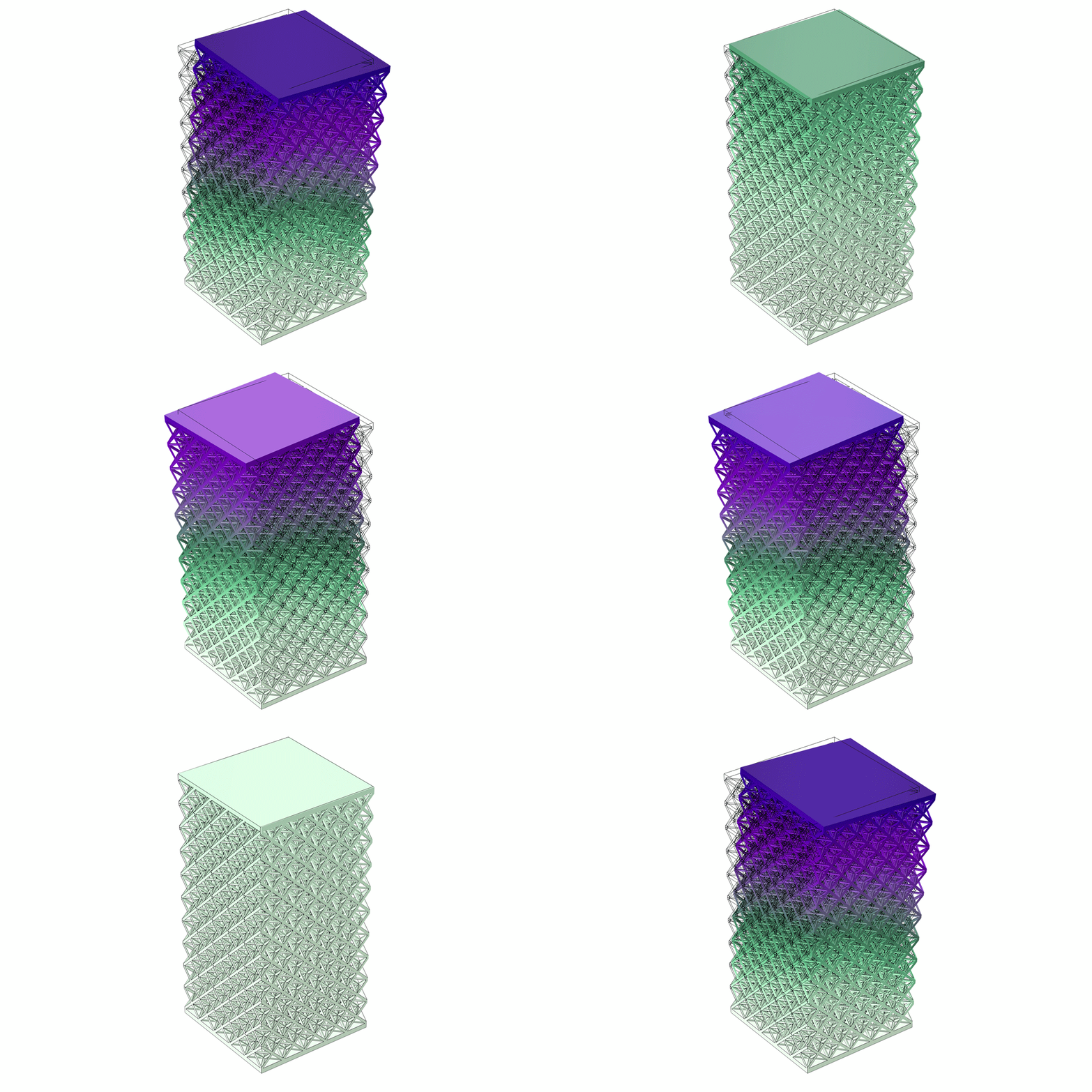
“With the promise of mRNA technologies being realized with the Covid vaccines, we thought that this would be a fantastic opportunity to see if C3d might also be able to play a role as an adjuvant in mRNA vaccine systems,” Jiang says.

To that end, the researchers engineered the mRNA to encode the C3d protein fused to the antigen, so that both components are produced as one protein by cells that receive the vaccine.
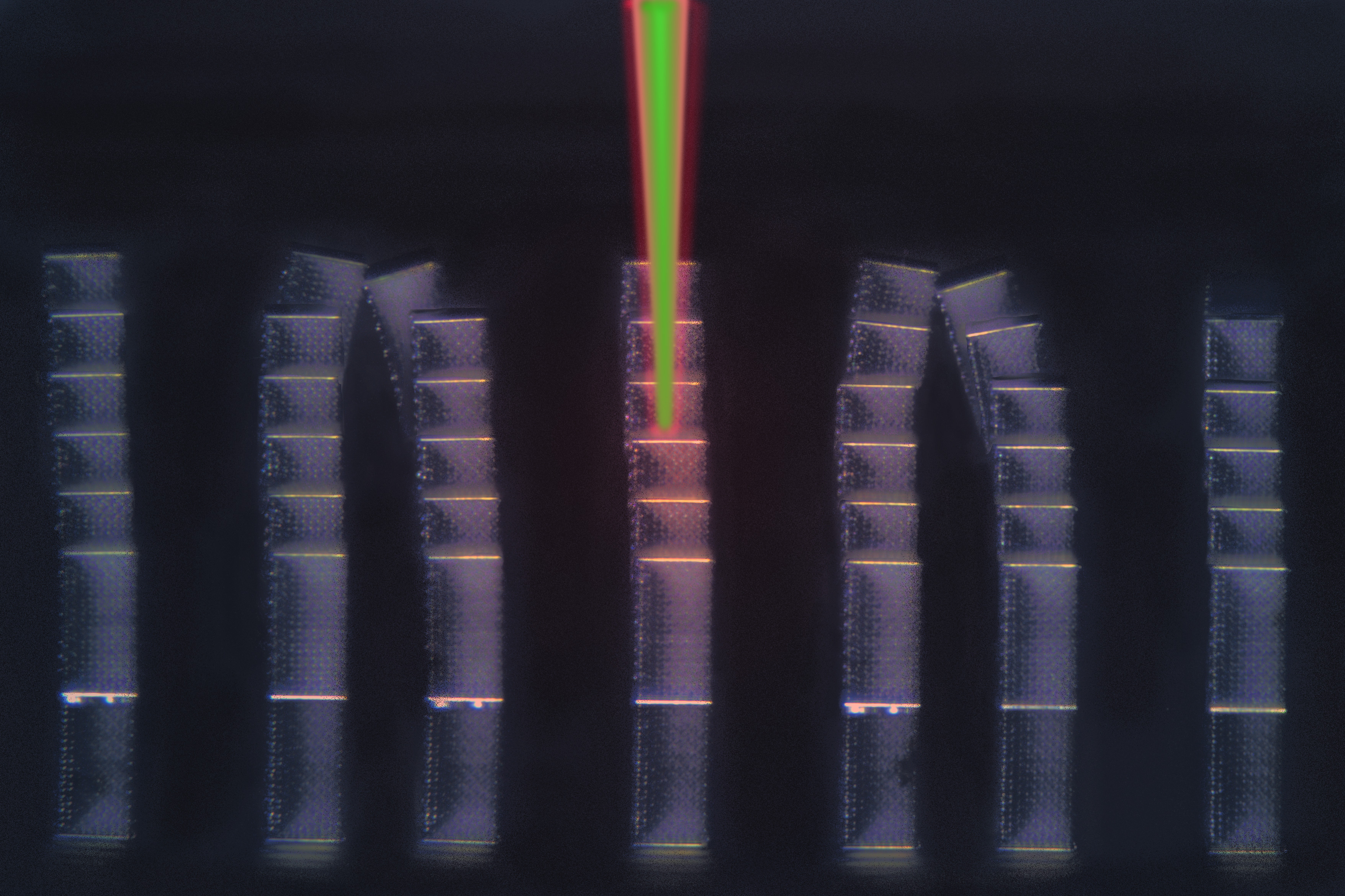
In the second phase of their strategy, the researchers modified the lipid nanoparticles used to deliver the RNA vaccine, so that in addition to helping with RNA delivery, the lipids also intrinsically stimulate a stronger immune response.

To identify lipids that would work best, the researchers created a library of 480 lipid nanoparticles with different types of chemistries. All of these are “ionizable” lipids, which become positively charged when they enter acidic environments. The original Covid RNA vaccines also included some ionizable lipids because they help the nanoparticles to self-assemble with RNA and they help target cells to take up the vaccine.
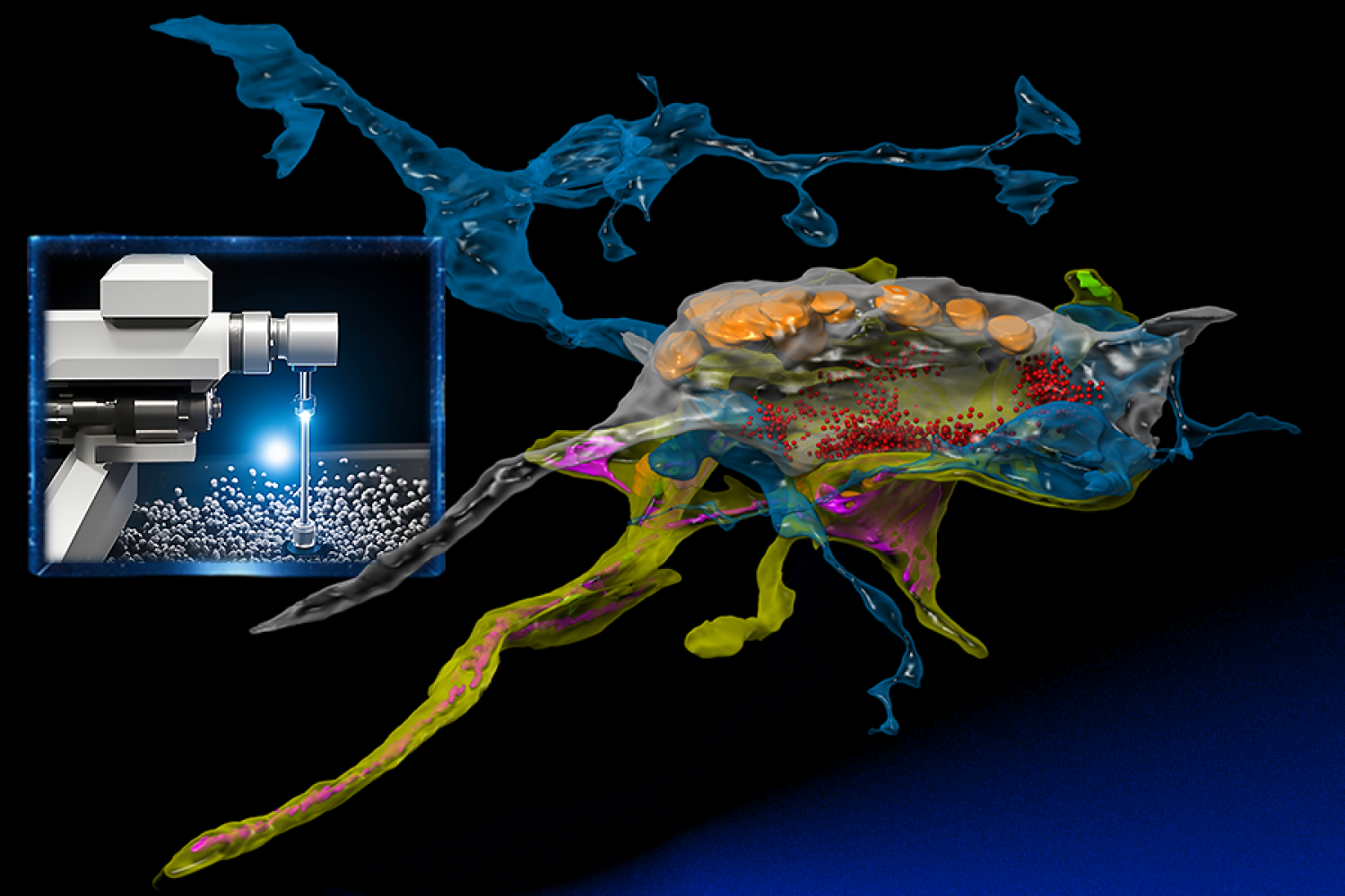
“We understood that nanoparticles themselves could be immunostimulatory, but we weren't quite sure what the chemistry was that was needed to optimize that response. So instead of trying to make the perfect one, we made a library and evaluated them, and through that we identified some chemistries that seemed to improve their response,” Anderson says.

Toward intranasal vaccines

The researchers tested their new vaccine, which included both RNA-encoded C3d and a top-performing ionizable lipid identified from their library screen, in mice. They found that mice injected with this vaccine produced 10 times more antibodies than mice given unadjuvanted Covid RNA vaccines. The new vaccine also provoked a stronger response among T cells, which play important roles in combating the SARS-CoV-2 virus.
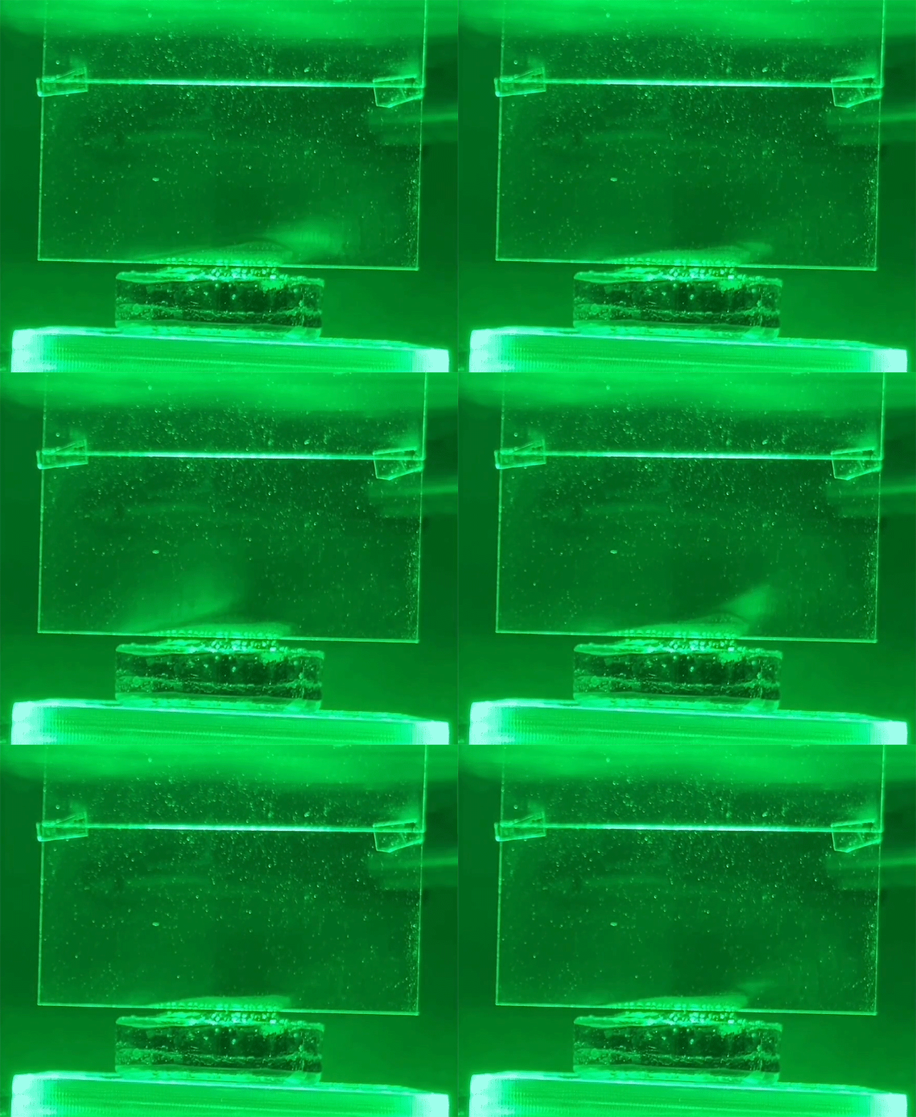
“For the first time, we’ve demonstrated a synergistic boost in immune responses by engineering both the RNA and its delivery vehicles,” Li says. “This prompted us to investigate the feasibility of administering this new RNA vaccine platform intranasally, considering the challenges presented by the mucociliary blanket barrier in the upper airways.”

When the researchers delivered the vaccine intranasally, they observed a similarly strong immune response in the mice. If developed for use in people, an intranasal vaccine could potentially offer enhanced protection against infection because it would generate an immune response within the mucosal tissues that line the nasal passages and lungs. 

Because self-adjuvanting vaccines elicit a stronger response at a lower dose, this approach could also help to reduce the cost of vaccine doses, which might allow them to reach more people, especially in developing nations, the researchers say.

Anderson’s lab is now exploring whether this self-adjuvanting platform might also help boost the immune response of other types of RNA vaccines, including cancer vaccines. Working with health care companies, the researchers also plan to test the effectiveness and safety of these new vaccine formulations in larger animal models, in hopes of eventually testing them in patients.
The research was funded by the National Institutes of Health and Translate Bio.

© Image: Jose-Luis Olivares, MIT with figures from iStock

By adding synergistic self-adjuvanting properties to Covid-19 RNA vaccines, MIT researchers have found a new approach that could lead to intranasal vaccines for Covid-19 and other respiratory diseases.
How to prevent biofilms in space

After exposure in space aboard the International Space Station, a new kind of surface treatment significantly reduced the growth of biofilms, scientists report. Biofilms are mats of microbial or fungal growth that can clog hoses or filters in water processing systems, or potentially cause illness in people.

In the experiment, researchers investigated a variety of surfaces treated in different ways and exposed to a bacteria called Pseudomonas aeruginosa, which is an opportunistic pathogen than can cause infections in humans, especially in hospitals. The surfaces were incubated for three days aboard the space station, starting in 2019. The results show that textured surfaces impregnated with a lubricant were highly successful at preventing biofilm growth during their long exposure in space. The findings are described in a paper in the journal Nature Microgravity, by Samantha McBride PhD ’20 and Kripa Varanasi of MIT, Pamela Flores and Luis Zea at the University of Colorado, and Jonathan Galakza at NASA Ames Research Center.

Clogs in water recovery system hoses aboard the ISS have been so severe at times, the hoses had to be sent back to Earth for cleaning and refurbishing. And while it isn’t known whether biofilms have directly contributed to astronaut illnesses, on Earth, biofilms are associated with 65 percent of microbial infections, and 80 percent of chronic infections, the researchers say.

One approach to preventing biofilms is to use surfaces coated with certain metals or oxides that kill microbes, but this approach can fail when a layer of dead microbes builds up on the surface and allows biofilm to form above it. But this was not the case with the liquid-infused surface that performed well in the ISS experiments: Rather than killing the microbes, it prevented them from adhering to the surface in the first place.

The specific surface used was made of silicon that was etched to produce a nanoscale forest of pillars. This spiky surface is then infused with a silicon oil, which is drawn into the texture and held in place by capillary action, leaving a smooth and highly slippery surface that significantly reduces the adhesion of microbes and prevents them from forming a biofilm.

Identical experiments were conducted on Earth as well as on the space station to determine the differences produced by the microgravity environment in orbit. To the researchers' surprise, the liquid-infused surface performed even better in space than it did on Earth at preventing microbial adhesion.

On previous and current space stations, including the USSR’s Mir station, Salyut 6, and Salyut 7,  as well as the International Space Station, “they’ve seen these biofilms, and they jeopardize a variety of instruments or equipment, including space suits, recycling units, radiators, and water treatment facilities, so it’s a very important problem that needed to be understood,” says Varanasi, a professor of mechanical engineering and founder of a company called LiquiGlide, which makes liquid-impregnated surfaces for containers to help their contents slide out.

Previous tests on Earth had shown that these treated surfaces could significantly reduce biofilm adhesion. When the samples from the space station were retrieved and tested, “we found that these surfaces are extremely good at preventing biofilm formation in the space station as well,” Varanasi says. This is important because past work has found that microgravity can have a significant influence on biofilm morphologies, attachment behavior, and gene expression, according to McBride. Thus, strategies that work well on Earth for biofilm mitigation may not necessarily be applicable to microgravity situations.

Preventing biofilms will be especially important for future long-duration missions, such as to the moon or Mars, where the option of quickly returning fouled equipment or sick astronauts to Earth will not be available, the team says. If further testing confirms its long-term stability and successful biofilm prevention, coatings based on the liquid-treated surface concept could be applied to a variety of critical components that are known to be susceptible to biofilm fouling, such as water treatment hoses and filters, or to parts that come in close contact with astronauts, such as gloves or food preparation surfaces.

In the terrestrial samples, biofilm formation was reduced by about 74 percent, while the space station samples showed a reduction of about 86 percent, says Flores, who did much of the testing of the ISS-exposed samples. “The results we got were surprising,” she says, because earlier tests carried out by others had shown biofilm formation was actually greater in space than on Earth. “We actually found the opposite on these samples,” she says.

While the tests used a specific and well-studied gram-negative kind of bacteria, she says, the results should apply to any kind of gram-negative bacteria, and likely to gram-positive bacteria as well. They found that the areas of the surface where no bacterial growth took place were covered by a thin layer of nucleic acids, which have a slight negative electric charge that may have helped to prevent microbes from adhering. Both gram-positive and gram-negative bacteria have a slight negative charge, which could repel them from that negatively charged surface, Flores says.

Other types of anti-fouling surfaces, Varanasi says, “work mostly on a biocidal property, which usually only works for a first layer of cells because after those cells die they can form a deposit, and microbes can grow on top of them. So, usually it’s been a very hard problem.” But with the liquid-impregnated surface, where what is exposed is mostly just the liquid itself, there are very few defects or points where the bacteria can find a footing, he says.

Although the test material was on the space station for more than a year, the actual tests were only performed over a three-day period because they required active participation by the astronauts whose schedules are always very busy. But one recommendation the team has made, based on these initial results, is that longer-duration tests should be carried out on a future mission. In these first tests, Flores says, the results after the third day looked the same as after the first and second days. “We don’t know for how long it will be able to keep up this performance, so we definitely recommend a longer time of incubation, and also, if possible, a continuous analysis, and not just end points.”

Zea, who initiated the project with NASA, says that this was the first time the agency has conducted tests that involved joint participation by two of its science programs, biology and physical sciences. “I think it stresses the importance of multidisciplinarity because we need to be able to combine these different disciplines to find solutions to real world problems.”

Biofilms are also a significant medical issue on Earth, especially on medical devices or implants including catheters, where they can lead to significant disease problems. The same kind of liquid-impregnated surfaces may have a role to play in helping to address these issues, Varanasi says.

The project was supported by NASA and used facilities provided by several other companies and organizations.

© Image: Space Biofilm Program

Inside these vials are chambers containing the new surface material and the microbes. They were launched in stasis to ISS to avoid bacterial growth before reaching microgravity conditions. Once in ISS, the astronauts activated the samples by combining the various chambers in the vials.
Arrays of quantum rods could enhance TVs or virtual reality devices

Flat screen TVs that incorporate quantum dots are now commercially available, but it has been more difficult to create arrays of their elongated cousins, quantum rods, for commercial devices. Quantum rods can control both the polarization and color of light, to generate 3D images for virtual reality devices.

Using scaffolds made of folded DNA, MIT engineers have come up with a new way to precisely assemble arrays of quantum rods. By depositing quantum rods onto a DNA scaffold in a highly controlled way, the researchers can regulate their orientation, which is a key factor in determining the polarization of light emitted by the array. This makes it easier to add depth and dimensionality to a virtual scene.

“One of the challenges with quantum rods is: How do you align them all at the nanoscale so they’re all pointing in the same direction?” says Mark Bathe, an MIT professor of biological engineering and the senior author of the new study. “When they’re all pointing in the same direction on a 2D surface, then they all have the same properties of how they interact with light and control its polarization.”

MIT postdocs Chi Chen and Xin Luo are the lead authors of the paper, which appears today in Science Advances. Robert Macfarlane, an associate professor of materials science and engineering; Alexander Kaplan PhD ’23; and Moungi Bawendi, the Lester Wolfe Professor of Chemistry, are also authors of the study.

Nanoscale structures

Over the past 15 years, Bathe and others have led in the design and fabrication of nanoscale structures made of DNA, also known as DNA origami. DNA, a highly stable and programmable molecule, is an ideal building material for tiny structures that could be used for a variety of applications, including delivering drugs, acting as biosensors, or forming scaffolds for light-harvesting materials.

Bathe’s lab has developed computational methods that allow researchers to simply enter a target nanoscale shape they want to create, and the program will calculate the sequences of DNA that will self-assemble into the right shape. They also developed scalable fabrication methods that incorporate quantum dots into these DNA-based materials.

In a 2022 paper, Bathe and Chen showed that they could use DNA to scaffold quantum dots in precise positions using scalable biological fabrication. Building on that work, they teamed up with Macfarlane’s lab to tackle the challenge of arranging quantum rods into 2D arrays, which is more difficult because the rods need to be aligned in the same direction.

Existing approaches that create aligned arrays of quantum rods using mechanical rubbing with a fabric or an electric field to sweep the rods into one direction have had only limited success. This is because high-efficiency light-emission requires the rods to be kept at least 10 nanometers from each other, so that they won’t “quench,” or suppress, their neighbors’ light-emitting activity.

To achieve that, the researchers devised a way to attach quantum rods to diamond-shaped DNA origami structures, which can be built at the right size to maintain that distance. These DNA structures are then attached to a surface, where they fit together like puzzle pieces.

“The quantum rods sit on the origami in the same direction, so now you have patterned all these quantum rods through self-assembly on 2D surfaces, and you can do that over the micron scale needed for different applications like microLEDs,” Bathe says. “You can orient them in specific directions that are controllable and keep them well-separated because the origamis are packed and naturally fit together, as puzzle pieces would.”

Assembling the puzzle

As the first step in getting this approach to work, the researchers had to come up with a way to attach DNA strands to the quantum rods. To do that, Chen developed a process that involves emulsifying DNA into a mixture with the quantum rods, then rapidly dehydrating the mixture, which allows the DNA molecules to form a dense layer on the surface of the rods.

This process takes only a few minutes, much faster than any existing method for attaching DNA to nanoscale particles, which may be key to enabling commercial applications.

“The unique aspect of this method lies in its near-universal applicability to any water-loving ligand with affinity to the nanoparticle surface, allowing them to be instantly pushed onto the surface of the nanoscale particles. By harnessing this method, we achieved a significant reduction in manufacturing time from several days to just a few minutes,” Chen says.

These DNA strands then act like Velcro, helping the quantum rods stick to a DNA origami template, which forms a thin film that coats a silicate surface. This thin film of DNA is first formed via self-assembly by joining neighboring DNA templates together via overhanging strands of DNA along their edges.

The researchers now hope to create wafer-scale surfaces with etched patterns, which could allow them to scale their design to device-scale arrangements of quantum rods for numerous applications, beyond only microLEDs or augmented reality/virtual reality.

“The method that we describe in this paper is great because it provides good spatial and orientational control of how the quantum rods are positioned. The next steps are going to be making arrays that are more hierarchical, with programmed structure at many different length scales. The ability to control the sizes, shapes, and placement of these quantum rod arrays is a gateway to all sorts of different electronics applications,” Macfarlane says.

“DNA is particularly attractive as a manufacturing material because it can be biologically produced, which is both scalable and sustainable, in line with the emerging U.S. bioeconomy. Translating this work toward commercial devices by solving several remaining bottlenecks, including switching to environmentally safe quantum rods, is what we’re focused on next,” Bathe adds.

The research was funded by the Office of Naval Research, the National Science Foundation, the Army Research Office, the Department of Energy, and the National Institute of Environmental Health Sciences.

© Image: Dr. Xin Luo, Bathe BioNanoLab

MIT engineers have used DNA origami scaffolds to create precisely structured arrays of quantum rods, which could be incorporated into LEDs for televisions or virtual reality devices.

Q&A: A high-tech take on Wagner’s “Parsifal” opera

The world-famous Bayreuth Festival in Germany, annually centered around the works of composer Richard Wagner, launched this summer on July 25 with a production that has been making headlines. Director Jay Scheib, an MIT faculty member, has created a version of Wagner’s celebrated opera “Parsifal” that is set in an apocalyptic future (rather than the original Medieval past), and uses augmented reality headset technology for a portion of the audience, among other visual effects. People using the headsets see hundreds of additional visuals, from fast-moving clouds to arrows being shot at them. The AR portion of the production was developed through a team led by designer and MIT Technical Instructor Joshua Higgason.

The new “Parsifal” has engendered extensive media attention and discussion among opera followers and the viewing public. Five years in the making, it was developed with the encouragement of Bayreuth Festival general manager Katharina Wagner, Richard Wagner’s great-granddaughter. The production runs until Aug. 27, and can also be streamed on Stage+. Scheib, the Class of 1949 Professor in MIT’s Music and Theater Arts program, recently talked to MIT News about the project from Bayreuth.

Q: Your production of “Parsifal” led off this year’s entire Bayreuth festival. How’s it going?

A: From my point of view it’s going quite swimmingly. The leading German opera critics and the audiences have been super-supportive and Bayreuth makes it possible for a work to evolve … Given the complexity of the technical challenge of making an AR project function in an opera house, the bar was so high, it was a difficult challenge, and we’re really happy we found a way forward, a way to make it work, and a way to make it fit into an artistic process. I feel great.

Q: You offer a new interpretation of “Parsifal,” and a new setting for it. What is it, and why did you choose to interpret it this way?

A: One of the main themes in “Parsifal” is that the long-time king of this holy grail cult is wounded, and his wound will not heal. [With that in mind], we looked at what the world was like when the opera premiered in the late 19th century, around the time of what was known as the Great African Scramble, when Europe re-drew the map of Africa, largely based on resources, including mineral resources.

Cobalt remains [the focus of] dirty mining practices in the Democratic Republic of Congo, and is a requirement for a lot of our electronic objects, in particular batteries. There are also these massive copper deposits discovered under a Buddhist temple in Afghanistan, and lithium under a sacred site in Nevada. We face an intense challenge in climate change, and the predictions are not good. Some of our solutions like electric cars require these materials, so they’re only solutions for some people, while others suffer [where minerals are being mined]. We started thinking about how wounds never heal, and when the prospect of creating a better world opens new wounds in other communities. … That became a theme. It also comes out of the time when we were making it, when Covid happened and George Floyd was murdered, which created an opportunity in the U.S. to start speaking very openly about wounds that have not healed.

We set it in a largely post-human environment, where we didn’t succeed, and everything has collapsed. In the third act, there’s derelict mining equipment, and the holy water is this energy-giving force, but in fact it’s this lithium-ion pool, which gives us energy and then poisons us. That’s the theme we created.

Q: What were your goals about integrating the AR technology into the opera, and how did you achieve that?

A: First, I was working with my collaborator Joshua Higgason. No one had ever really done this before, so we just started researching whether it was possible. And most of the people we talked to said, “Don’t do it. It’s just not going to work.” Having always been a daredevil at heart, I was like, “Oh, come on, we can figure this out.”

We were diligent in exploring the possibilities. We made multiple trips to Bayreuth and made these milimeter-accurate laser scans of the auditorium and the stage. We built a variety of models to see how to make AR work in a large environment, where 2,000 headsets could respond simultaneously. We built a team of animators and developers and programmers and designers, from Portugal to Cambridge to New York to Hungary, the UK, and a group in Germany. Josh led this team, and they got after it, but it took us the better part of two years to make it possible for an audience, some of whom don’t really use smartphones, to put on an AR headset and have it just work.

I can’t even believe we did this. But it’s working.

Q: In opera there’s hopefully a productive tension between tradition and innovation. How do you think about that when it comes to Wagner at Bayreuth?

A: Innovation is the tradition at Bayreuth. Musically and scenographically. “Parsifal” was composed for this particular opera house, and I’m incredibly respectful of what this event is made for. We are trying to create a balanced and unified experience, between the scenic design and the AR and the lighting and the costume design, and create perfect moments of convergence where you really lose yourself in the environment. I believe wholly in the production and the performers are extraordinary. Truly, truly, truly extraordinary.

Q: People have been focused on the issue of bringing AR to Bayreuth, but what has Bayreuth brought to you as a director?

A: Working in Bayreuth has been an incredible experience. The level of intellectual integrity among the technicians is extraordinary. The amount of care and patience and curiosity and expertise in Bayreuth is off the charts. This community of artists is the greatest. … People come here because it’s an incredible meeting of the minds, and for that I’m immensely filled with gratitude every day I come into the rehearsal room. The conductor, Pablo Heras-Casado, and I have been working on this for several years. And the music is still first. We’re setting up technology not to overtake the music, but to support it, and visually amplify it.

It must be said that Katharina Wagner has been one of the most powerfully supportive artistic directors I have ever worked with. I find it inspiring to witness her tenacity and vision in seeing all of this through, despite the hurdles. It’s been a great collaboration. That’s the essence: great collaboration.

This work was supported, in part, by an MIT.nano Immersion Lab Gaming Program seed grant, and was developed using capabilities in the Immersion Lab. The project was also funded, in part, by a grant from the MIT Center for Art, Science, and Technology.

© Image: Enrico Nawrath. Courtesy of the Bayreuther Festival

Director and MIT Professor Jay Scheib speaks about his widely heralded production of Wagner’s “Parsifal” opera at the Bayreuth Festival, which features an apocalyptic theme and augmented reality headsets for the audience.
❌