FreshRSS

Zobrazení pro čtení

Jsou dostupné nové články, klikněte pro obnovení stránky.

Western Digital: We Are Sampling 32TB SMR Hard Drives

In an unexpected announcement during their quarterly earnings call this week, Western Digital revealed that it has begun sampling an upcoming 32TB hard drive. The nearline HDD is aimed at hyperscalers, and relies on a combination of Westen Digital's EAMR technology, as well as shingled magnetic recording (SMR) technology to hit their highest capacity figures to date.

Western Digital's 32TB HDD uses all of the company's most advanced technologies. Besides energy-assisted magnetic recording (EAMR/ePMR 2 to be more precise) technology, WD is also leveraging triple-stage actuators for better positioning of heads and two-dimensional (TDMR) read heads, OptiNAND for extra performance and reliability, distributed sector (DSEC) technology and a proprietary error correcting code (ECC) technology. And, most importantly, UltraSMR technology to provide additional capacity.

"We are shipping samples of our 32TB UltraSMR/ePMR nearline hard drives to select customers," said David Goeckeler, chief executive of Western Digital, at the earnings call. "These drives feature advanced triple-stage actuators and OptiNAND technology which are designed for seamless qualification, integration and deployment in hyperscale cloud and enterprise data centers while maintaining exceptional reliability."

Seagate is currently shipping its 30TB Exos HDDs based on heat-assisted magnetic recording (HAMR) platform called Modaic 3+ to select exascalers, and the company has implied that it can build a 32TB version of the drive using SMR. Therefore, from capacity point of view, Western Digital's announcement means that the company has caught up with its rival.

As with the comapny's other UltraSMR drives, the 32TB nearline drive is aimed at WD's enterprise customers, whose infrastructure can handle the additional management requirements that SMR imposes. As SMR in enterprise drives is not transparent, it's up to the host to manage many of the complexities that come with a hard drive that isn't suited for random writes. Though at least in WD's case, the upshot is that UltraSMR also offers a more significant density increase than other SMR implementations, using a larger number of SMR bands to increase HDD capacity by up to 20%.

Working backwards, that 20% capacity increase also means that WD's new drive is starting from 2.56TB CMR platters. And while 2.56TB makes for a very decent areal density, this would mean that WD is still behind rival Seagate in terms of areal density overall, as Seagate has 3TB CMR platters in its latest HAMR-based Exos drives.

ECS LIVA Z5 PLUS mini-PC Review: A Different Take on Raptor Lake

The trend towards miniaturization of desktop systems was kickstarted by the Intel NUCs in the early 2010s. The increasing popularity of compact PCs also led to the introduction of a variety of slightly larger form-factors. Custom boards falling in size between the NUC's 4" x 4" ultra-compact form-factor (UCFF) and industrial-applications oriented 3.5" SBC have also gained traction. The ECS LIVA Z5 PLUS is one such system, designed and marketed towards business and industrial use-cases.

Intel's Raptor Lake series of products was introduced in early 2023. It came in both P and U versions for notebooks and ultraportables, in addition to the usual H(X) ones for high-performance gaming notebooks. Most mini-PCs and NUCs opted for the P varieties in their systems. The ECS LIVA Z5 PLUS represents a different take, with a U series processor operating with a slight increase in the configurable TDP (cTDP) over Intel's suggested 15W operating point. Read on for a comprehensive look at the performance and features of the ECS LIVA Z5 PLUS, including some comments on the benefits enabled by the slightly larger form-factor.

Intel Extends 13th & 14th Gen Core Retail CPU Warranties By 2 Years In Response to Chip Instability Issues

Capping off an extensive (and expensive) week for Intel, the company has also announced that they are taking additional steps to address the ongoing chip stability issues with desktop Raptor Lake chips – the 13th and 14th Generation desktop Core processors. In order to keep owners whole, Intel will be extending the warranty on retail boxed Raptor Lake chips by two years, bringing the cumulative warranty for the chips to five years altogether.

This latest announcement comes as Intel is still in the process of preparing their major Raptor Lake microcode update, which is designed to mitigate the issue (or rather, further damage) by fixing the elevated voltage bug in their existing microcode that has led to the issue in the first place. That microcode update remains scheduled for mid-August, roughly a couple of weeks from now.

But until then – and depending on how quickly the update is distributed, even afterwards – there is still the matter of what to do with Raptor Lake desktop chips that are already too far gone and are consequently unstable. Intel’s retail boxed Raptor Lake chips ship with a 3 year warranty, which given the October 2022 launch date, would have the oldest of these chips covered until October of 2025 – a bit over a year from now. And while the in-development fix should mean that this is plenty of time to catch and replace any damaged chips, Intel has opted to take things one step further by extending the chips’ warranty to five years.

Overall, this is much-needed bit of damage control by Intel to restore some faith in their existing Raptor Lake desktop processor lineup. Even with the planned microcode fix, it remains unclear at best about what the long-term repercussions of the voltage bug is, and what it means for the lifespan of still-stable chips that receive the fixed microcode. In the best-case scenario, an extended warranty gives Raptor Lake owners a bit more peace of mind, and in a worst-case scenario, they’re now covered for a couple of years longer if the chip degradation issues persist.

One important thing to note, however, is that the extended warranty will only apply to boxed processors, i.e. Intel’s official retail chips. Intel’s loose chips that are sold by the tray to OEMs and certain distributors – commonly referred to as “tray” processors – are not covered by the extended warranty. While Raptor Lake tray processors do technically come with a three-year warranty of their own, Intel does not provide direct, end-user warranty service for these chips. Instead, those warranties are serviced by the OEM or distributor that sold the chip.

With the bulk of Intel’s chips going to OEMs and other professional system builders, Intel will undoubtedly need to settle things with those groups, as well. But with OEM dealings typically remaining behind closed doors, it’s unlikely we’ll hear about just what is agreed there. Regardless, whatever Intel does (or doesn’t do) to assuage OEMs and distributors, those groups will remain responsible for handling warranty claims for tray chips.

Finally, it should be noted that while today’s announcement outlines the two-year warranty extension, it doesn’t deliver the full details on the program. Intel expects to release more details on the extended warranty program “in the coming days.”

Intel’s full statement is below:

Intel is committed to making sure all customers who have or are currently experiencing instability symptoms on their 13th and/or 14th Gen desktop processors are supported in the exchange process. We stand behind our products, and in the coming days we will be sharing more details on two-year extended warranty support for our boxed Intel Core 13th and 14th Gen desktop processors.

In the meantime, if you are currently or previously experienced instability symptoms on your Intel Core 13th/14th Gen desktop system:
  • For users who purchased systems from OEM/System Integrators – please reach out to your system manufacturer’s support team for further assistance.
  • For users who purchased a boxed CPU – please reach out to Intel Customer Support for further assistance.
At the same time, we apologize for the delay in communications as this has been a challenging issue to unravel and definitively root cause.
-Intel Community Post

Additional Details on Via Oxidation Issue

Separately, Intel’s community team also posted a brief update on the via oxidation issue that, although distinct from the current Raptor Lake instability issues, came into question at roughly the same time. Intel has previously stated that that issue is unconnected to the ongoing stability issues, and was fixed back in 2023. And this latest update offers a few more details on just what that manufacturing issue entailed.

The Via Oxidation issue currently reported in the press is a minor one that was addressed with manufacturing improvements and screens in early 2023.

The issue was identified in late 2022, and with the manufacturing improvements and additional screens implemented Intel was able to confirm full removal of impacted processors in our supply chain by early 2024. However, on-shelf inventory may have persisted into early 2024 as a result.

Minor manufacturing issues are an inescapable fact with all silicon products. Intel continuously works with customers to troubleshoot and remediate product failure reports and provides public communications on product issues when the customer risk exceeds Intel quality control thresholds.
-Intel Community Post

Update: Intel Accelerated Ireland EUV Fab Ramp-Up as Meteor Lake Chips Were In Short Supply

Update 08/02: Patrick Moorhead has published a further tweet, clarifying that "Pat [Gelsinger] didn’t tell me l that there were yield issues. This was *my* interpretation." The text of the article has been updated accordingly to reflect this tweet, as well as Intel statements about accelerating their Ireland Fab 34 ramp-up.


Alongside Intel’s weak Q2 2024 earnings report and the announcement of $10 billion in spending cuts and layoffs for 2025, the company is also disclosing some new information about their chip deliveries over the first half of the year. A brief report, posted on X by analyst Patrick Moorhead and citing a conversation with Intel CEO Pat Gelsinger, revealed that Intel encountered a major production bottleneck on Meteor Lake earlier this year. The issue was significant enough to drive intel to take the extraordinary and costly step of accelerating their Ireland fab ramp-up in order to improve chip capacity.

It was a very rough Q2 for $INTC. And that guide... Thanks, @Pgelsinger, for the time to discuss.

It appears that there were yield/throughput issues on Meteor Lake, negatively impacting gross margins. When you have to get the product to your customers, and you have wafers to… pic.twitter.com/pHU66xvFe7

— Patrick Moorhead (@PatrickMoorhead) August 1, 2024
It appears that there were yield/throughput issues on Meteor Lake, negatively impacting gross margins. When you have to get the product to your customers, and you have wafers to burn, you run it hot. I heard from OEMs that they needed more MTL, but it wasn't bone dry. You have to run hot lots in that case, or else your customers will be impacted. I didn't have this one on my dance card.
-Patrick Moorhead

In a separate tweet posted several hours later, Moorhead then clarified that the yield issues mentioned in his first tweet were his interpretation of the matter, rather than something Pat Gelsinger had told him directly.

For the record, Pat didn’t tell me l that there were yield issues. This was *my* interpretation. But when your COGS are cited for a specific product are rising in a big, big way, with MTL, you *have* to surmise either yield or back end throughout issues that can be very expensive.
-Patrick Moorhead

Decoding Moorhead’s dense tweets, fundamentally, Moorhead is questioning why Intel's Cost of Goods Sold (COGS) – how much the company's chips cost to produce – were on the rise with the launch of Meteor Lake.  The analyst surmised that yields and/or some other unexpected production bottleneck must be the case, as these are the typical issues that drive up chip COGS on a short-term basis like Intel has been experiencing.

And, judging from Intel's earnings call that took place after the initial tweet, Moorhead was right to an extent. Referencing the increased COGS, Intel CFO David Zinsner noted that Intel opted to ramp up its high-volume production in Ireland faster than initially planned. This increased Intel's capacity for Intel 4 (and Intel 3) capacity, but doing so also increased their costs, as wafers out of Ireland cost more in the near term.

The largest impact was caused by an accelerated ramp of our AI PC product. In addition to exceeding expectations on Q2 Core Ultra shipments, we made the decision to accelerate transition of Intel 4 and 3 wafers from our development fab in Oregon to our high volume facility in Ireland, where wafer costs are higher in the near term.
-Intel CFO David Zinsner (Intel Q2'24 Earnings Call)

Between Moorhead's report that OEMs have been receiving fewer Meteor Lake chips than they could use, and Intel's announcement that they accelerated the Ireland fab ramp-up, this is the first significant disclosure that Meteor Lake chips were, at least at some point, in unexpectedly short supply. Which in turn required Intel to take unexpected and extraordinary steps in order to improve chip production, at the cost of lower short-term profit margins and higher COGS.

The first of Intel's high-volume manufacturing (HVM) fabs to be equipped for the Intel 4 and Intel 3 processes, Fab 34 in Ireland is a critical element to Intel's cutting-edge product plans over the next couple years. Intel was not initially planning on relying so much on Fab 34 this soon – instead using their Oregon development fabs to do more of their Intel 4 & Intel 3 fabrication – but the company opted to ramp up at a faster pace. The benefit to Intel is that they get more fab capacity sooner, but it means they're incurring around $1 billion in costs now of what would have otherwise been spread out over further quarters during a more gradual ramp-up.

The net result was that, while Intel took a margin hit, it also allowed them to supply more Meteor Lake chips than they otherwise would have, even beating their own previous projections for Q2 shipments. Overall, Intel reported in their Q2 earnings that they’ve shipped 15 million “AI PC” chips since Meteor Lake’s launch, though the company doesn't break down how many of those were in Q2 versus Q1 and Q4'23. Still, according to Moorhead, this was fewer chips than OEMs would have liked to have, and they would have taken more chips if they were available.

COGS and Ireland ramp-ups aside, Moorhead also posits that some of Intel's capacity boost came from running “hot lots” of Meteor Lake – high priority wafer batches that get moved to the front of the line in order to be processed as soon as possible (or as reasonably close as is practical). Hot lots are typically used to get highly-demanded chips produced quickly, getting them through a fab sooner than the normal process would take. As a business tool, hot lots are a fact of life of chip production, but they’re undesirable because in most cases they cause disruptions to other wafers that are waiting their turn to be processed.

If true, running hot lots of Meteor Lake would be a significant development given the potential disruptions. At the same time, however, the situation with Meteor Lake is somewhat particular, as the Intel 4 process used for Meteor Lake’s compute tile (the only active tile made at Intel) is not offered to external foundry customers, or even used by other Intel CPUs (Xeon 6s all use Intel 3). So hot lots of Meteor Lake would have few other wafers to even jump ahead of for EUV tooling (Intel would certainly not put them ahead of high-margin Xeon products), while it's unclear how this would cascade down to any tools shared with Intel 7.

Intel, for their part, did not comment on Meteor Lake chip yields or hot lots in their earnings call.

In any case, Intel at this point is looking to turn around their troubled fortunes in the second half of this year. The company’s next-gen client SoC for mobile, Lunar Lake, is set to launch on September 3rd. And notably, both of its active tiles are being built by TSMC. So Lunar Lake would be spared from any Intel logic fab bottlenecks, though it still has to go through Intel’s facilities for assembly using their Foveros technology. And there remains the thorny issue of higher production costs altogether, since Intel is paying for what's effectively the fully outsourced production of a Core CPU.

Intel Bleeds Red, Plans 15% Workforce Layoff and $10B Cuts For 2025

Amidst the backdrop of a weak quarterly earnings report that saw Intel lose money for the second quarter in a row, Intel today has announced that the company will be cutting costs by $10 billion in 2025 in an effort to bring Intel back to profitability. The cuts will touch almost every corner of the company in some fashion, with Intel planning to cut spending on R&D, marketing, administration, and capital expenditures. The most significant of these savings will come from a planned 15% reduction in force, which will see Intel lay off 15,000 employees over the next several months – thought to be one of Intel’s biggest layoffs ever.

In an email to Intel’s staff, which was simultaneously published to Intel’s website, company CEO Pat Gelsinger made the financial stakes clear: Intel is spending an unsustainable amount of money for their current revenues. Citing the company’s current costs, Gelsinger wrote that “our costs are too high, our margins are too low,“ and that “our annual revenue in 2020 was about $24 billion higher than it was last year, yet our current workforce is actually 10% larger now than it was then.” Consequently, Intel will be enacting a series of painful cuts to bring the company back to profitability.

Intel is not publicly disclosing precisely where those cuts will come from, but in the company’s quarterly earnings release, the company noted that it was targeting operating expenses, capital expenditures, and costs of sales alike.

For operating expenses, Intel will be cutting “non-GAAP R&D and marketing, general and administrative” spending, with a goal to trim that from $20 billion in 2024 to $17.5 billion in 2025. Meanwhile gross capital expenditures, a significant expense for Intel in recent years as the company has built up its fab network, are projected to drop from $25 billion to $27 billion for 2024, to somewhere between $20 billion and $23 billion in 2025. Compared to Intel’s previous plans for capital expenditures, this would reduce those costs by around 20%. And finally, the company is expecting to save $1 billion on the cost of sales in 2025.

Intel 2025 Spending Cuts
  2024 Projected Spending 2025 Projected Spending Projected Reduction
Operating Expenses
(R&D, Marketing, General, & Admin)
$20B $17.5B $2.5B
Capital Expenditures (Gross) $25B - $27B $20B - $23B $2B - $7B
Cost of Sales N/A $1B Savings $1B

Separately, in Intel’s email to its employees, Gelsinger outlined that these cuts will also require simplifying Intel’s product portfolio, as well as the company itself. The six key priorities for Intel will include cutting underperforming product lines, and cutting back Intel’s investment in new products to “fewer, more impactful projects”. Meanwhile on the administrative side of efforts, Intel is looking to eliminate redundancies and overlap there, as well as stopping non-essential work.

  • Reducing Operational Costs: We will drive companywide operational and cost efficiencies, including the cost savings and head count reductions mentioned above.
  • Simplifying Our Portfolio: We will complete actions this month to simplify our businesses. Each business unit is conducting a portfolio review and identifying underperforming products. We are also integrating key software assets into our business units so we accelerate our shift to systems-based solutions. And we will narrow our incubation focus on fewer, more impactful projects.
  • Eliminating Complexity: We will reduce layers, eliminate overlapping areas of responsibility, stop non-essential work, and foster a culture of greater ownership and accountability. For example, we will consolidate Customer Success into the Sales, Marketing and Communications Group to streamline our go-to-market motions.
  • Reducing Capital and Other Costs: With the completion of our historic five-nodes-in-four-years roadmap clearly in sight, we will review all active projects and equipment so we begin to shift our focus toward capital efficiency and more normalized spending levels. This will reduce our 2024 capital expenditures by more than 20%, and we plan to reduce our non-variable cost of goods sold by roughly $1 billion in 2025.
  • Suspending Our Dividend: We will suspend our stock dividend beginning next quarter to prioritize investments in the business and drive more sustained profitability.
  • Maintaining Growth Investments: Our IDM2.0 strategy is unchanged. Having fought hard to reestablish our innovation engine, we will maintain the key investments in our process technology and core product leadership.

The bulk of these cuts, in turn, will eventually come down to layoffs. As previously noted, Intel is planning to cut about 15% of its workforce. Just how many layoffs this will entail remains to be seen; Gelsinger’s letter puts it at roughly 15,000 employees, while Intel’s most recent published headcount would put this figure at closer to 17,000 employees.

Whatever the number, Intel is expecting to have most of the reductions completed by the end of this year. The company will be using a combination of early retirement packages and buy-outs, or what the company terms as “an application program for voluntary departures.”

Intel’s investors will be taking a hit, as well. The company’s generous quarterly dividend, a long-time staple of the chipmarker and one of the key tools to entice long-term investors, will be suspended starting in Q4 of 2024. With Intel losing money over multiple quarters, Intel cannot afford (or at least, cannot justify) paying out cash in the forms of dividends when that money could be getting invested in the company itself. Though as the long-term health of the company is still reliant on offering dividends, Intel says that the suspension will be temporary, as the company reiterated its “long-term commitment to a competitive dividend as cash flows improve to sustainably higher levels.” For Q2 2024, Intel paid out $0.125/share in dividends, or a total of roughly $0.5B.

Ultimately, the message coming from Intel today is that it is continuing (if not accelerating) its plans to slim down the company; to focus on a few areas of core competencies that suit the company’s abilities and its financial goals. Intel is throwing everything behind its IDM 2.0 initiative to regain process leadership and serve as a world-class contract foundry, and even with Intel’s planned spending cuts for 2025, that initiative will continue to move forward as planned.

On that note, cheering up investors in what’s otherwise a brutal report from the company, Intel revealed that they’ve achieved another set of key milestones with their in-development 18A process. The company released the 1.0 process design kit (PDK) to customers last month, and Intel has successfully powered-on their first Panther Lake and Clearwater Forest chips. 18A remains on track to be “manufacturing-ready” by the end of this year, with Intel looking to start wafer production in the first half of 2025. 18A remains a make-or-break technology for Intel Foundry, and the company as a whole, as this is the node that Intel expects to return them to process leadership – and from which they can improve upon to continue that leadership.

Sources: Intel Q2'24 Earnings, Intel Staff Letter

Best Buy Briefly Lists AMD's Ryzen 9000 CPUs: From $279 to $599

Although AMD delayed launch of its Ryzen 9000-series processors based on the Zen 5 microarchitecture from July 31, to early and mid-August, the company's partner (and major US retailer) Best Buy briefly began listing the new CPUs today, revealing a very plausible set of launch prices. As per the retailer's product catalog, the most affordable unlocked Zen 5-based processor will cost $279, whereas the highest-performing Zen 5-powered CPU will cost $599 at launch.

AMD will start its Ryzen 9000 series rollout from relatively inexpensive six-core Ryzen 5 9600X and eight-core Ryzen 7 9700X on August 8. Per the Best Buy listing, the Ryzen 5 9600X will cost $279, whereas the Ryzen 7 9700X will carry a recommended price tag of $359.  Meanwhile, The more advanced 12-core Ryzen 9 9900X and 16-core Ryzen 9 9950X will hit the market on August 15 at MSRPs of $449 and $599, respectively, based on the Best Buy listing.

AMD Ryzen 9000 Series Processors
Zen 5 Microarchitecture (Granite Ridge)
AnandTech Cores /
Threads
Base
Freq
Turbo
Freq
L2
Cache
L3
Cache
TDP MSRP
Ryzen 9 9950X 16C / 32T 4.3GHz 5.7GHz 16 MB 64 MB 170 W $599
Ryzen 9 9900X 12C / 24T 4.4GHz 5.6GHz 12 MB 64 MB 120 W $449
Ryzen 7 9700X 8C / 16T 3.8GHz 5.5GHz 8 MB 32 MB 65 W $359
Ryzen 5 9600X 6C / 12T 3.9GHz 5.4GHz 6 MB 32 MB 65 W $279

It is noteworthy that when compared to the launch prices of the Zen 4-based Ryzen 7000 processors, the new Zen 5-powered Ryzen 9000 CPUs come in cheaper. The range topping Ryzen 9 5950X started at $799 in 2020, while the Ryzen 9 7950X had a recommended $699 price tag in 2022. By contrast, the top-end Ryzen 9 9950X is listed at $599. Both Ryzen 7 5600X and Ryzen 7 7600X cost $299 at launch, while the upcoming Ryzen 5 9600X will apparently be priced at $279 at launch.

As always with accidental retailer listings, it should be emphasized that AMD has not yet announced official pricing for their Ryzen 9000 CPUs. Given Best Buy's status as one of the largest US electronics retailers, these prices carry a very high probability of being accurate; but none the less, they should be taken with a grain of salt – if only because last-minute price changes are not unheard of with new CPU launches.

Source: Best Buy (via @momomo_us)

Micron Ships Denser & Faster 276 Layer TLC NAND, Arriving First In Micron 2650 Client SSDs

Micron on Tuesday announced that the company has begun shipping its 9th Generation (G9) 276 layer TLC NAND. The next generation of NAND from the prolific memory maker, Micron's latest NAND is designed to further push the envelope on TLC NAND performance, offering significant density and performance improvements over its existing NAND technology.

Micron's G9 TLC NAND memory features 276 active layers, which is up from 232-layers in case of Micron's previous generation TLC NAND. At this point the company is being light on technical details in their official material. However in a brief interview with Blocks & Files, the company confirmed that their 276L NAND still uses a six plane architecture, which was first introduced with the 232L generation. At this point we're assuming Micron is also string-stacking two decks of NAND together, as they have been for the past couple of generations, which means we're looking at 138 layer decks.

Micron TLC NAND Flash Memory
  276L 232L
(B58R)
176L
(B47R)
Layers 276 232 176
Decks 2 (x138)? 2 (x116) 2 (x88)
Die Capacity 1 Tbit 1 Tbit 512 Gbit
Die Size (mm2) ~48.9mm2 ~70.1mm2 ~49.8mm2
Density (Gbit/mm2) ~21 14.6 10.3
I/O Speed 3.6 GT/s
(ONFi 5.1)
2.4 GT/s
(ONFi 5.0)
1.6 GT/s
(ONFI 4.2)
Planes 6 6 4
CuA / PuC Yes Yes Yes

On the density front, Micron told Blocks & Files that they have improved their NAND density by 44% over their 232L generation. Which, given what we know about that generation, would put the density at around 21 Gbit/mm2. Or for a 1Tbit die of TLC NAND, that works out to a die size of roughly 48.9mm2, comparable to the die size of a 512Gbit TLC die from Micron's older 176L NAND.

Besides improving density, the other big push with Micron's newest generation of NAND was further improving its throughput. While the company's 232L NAND was built against the ONFi 5.0 specification, which topped out at transfer rates of 2400 MT/sec, their new 276L NAND can hit 3600 MT/sec, which is consistent with the ONFi 5.1 spec.

Meanwhile, the eagle-eyed will likely also pick up on Micron's ninth-generation/G9 branding, which is new to the company. Micron's has not previously used this kind of generational branding for their NAND, which up until now has simply been identified by its layer count (and before the 3D era, its feature size). Internally, this is believed to be Micron's 7th generation 3D NAND architecture. However, taking a page from the logic fab industry, Micron seems to be branding it as ninth-generation in order to keep generational parity with its competitors, who are preparing their own 8th/9th generation NAND (and thus cliam that they are the first NAND maker to ship 9th gen NAND).

And while this NAND will eventually end up in all sorts of devices – including, no doubt, high-end PCIe Gen5 drives thanks to its high transfer rates – Micron's launch vehicle for the NAND is their own Micron 2650 client SSD. The 2650 is a relatively straightforward PCIe Gen4 x4 SSD, using an unnamed, DRAMless controller alongside Micron's new NAND. The company is offering it in 3 form factors – M.2 2280, 2242, and 2230 – with a modest set of capacities ranging from 256GB to 1TB.

Micron's 2650 NVMe SSDs offer sequential read performance of up to 7000 MB/s as well as sequential write performance of up to 6000 MB/s. As for random performance, we are talking about up to a million read and write IOPS, depending on the configuration.

Micron 2650 SSD Specifications
Capacity 1 TB 512 GB 256 GB
Controller PCIe Gen4 DRAMless
NAND Flash Micron G9 (276L) TLC NAND
Form-Factor, Interface Single-Sided M.2-2280/2242/2230
PCIe 4.0 x4, NVMe 1.4c
Sequential Read 7000 MB/s 7000 MB/s 5000 MB/s
Sequential Write 6000 MB/s 4800 MB/s 2500 MB/s
Random Read IOPS 1000K 740K 370K
Random Write IOPS 1000K 1000K 500K
SLC Caching Yes
TCG Opal Encryption 2.02
Write Endurance 600 TBW 300 TBW 200 TBW

The performance of the drives scales pretty significantly with capacity, underscoring how much parallelism is needed to keep up with the PCIe Gen4 controller. The rated capacity of the drives scales similarly, with the smallest drive rated for 200TBW (800 drive writes), while the largest drive is rated for 600 TBW (600 drive writes).

“The shipment of Micron G9 NAND is a testament to Micron’s prowess in process technology and design innovations,” said Scott DeBoer, executive vice president of Technology and Products at Micron. “Micron G9 NAND is up to 73% denser than competitive technologies in the market today, allowing for more compact and efficient storage solutions that benefit both consumers and businesses.”

Micron's G9 276-layer TLC NAND memory is also in qualification with customers in component form, so expect the company's partners to adopt it for their high-end SSDs in the coming quarters. In addition, Micron plans Crucial-branded SSDs based on its G9 NAND memory..

The Cooler Master V Platinum V2 1600W ATX 3.1 PSU Review: Quiet Giant

Continuing our ongoing look at the latest-generation ATX 3.1 power supplies, today we are examining Cooler Master's V Platinum 1600 V2, a recent addition to the company's expansive PSU lineup.

The V Platinum 1600 V2 is designed to cater to top-end gaming and workstation PCs while offering maximum compatibility with modern ATX directives. And while it boasts a massive 1600 Watt output and a long list of features, the V is a workhorse of a power supply rather than a flagship; Cooler Master is aiming the PSU at budget-conscious users who can't justify spending top dollar, but whom none the less need a powerful and relatively efficient (80PLUS Platinum) power supply.

So often we see PSU vendors go for broke on their high-wattage units, since there's a lot of overlap there with the premium market, so it will be interesting to see what Cooler Master can do with a slightly more modest bill of materials.

Intel to Launch "Lunar Lake" Core Ultra Chips on September 3rd

Intel’s next-generation Core Ultra laptop chips finally have a launch date: September 3rd.

Codenamed Lunar Lake, Intel has been touting the chips for nearly a year now. Most recently, Intel offered the press a deep dive briefing on the chips and their underlying architectures at Computex back in June, along with a public preview during the company’s Computex keynote. At the time Intel was preparing for Q3’2024 launch, and that window has finally been narrowed down to a single date – September 3rd – when Intel will be hosting their Lunar Lake launch event ahead of IFA.

Intel’s second stab at a high volume chiplet-based processor for laptop users, Lunar Lake is aimed particularly at ultrabooks and other low-power mobile devices, with Intel looking to wrestle back the title of the most efficient PC laptop SoC. Lunar Lake is significant in this respect as Intel has never previously developed a whole chip architecture specifically for low power mobile devices before – it’s always been a scaled-down version of a wider-range architecture, such as the current Meteor Lake (Core Ultra 100 series). Consequently, Intel has been touting that they’ve made some serious efficiency advancements with their highly targeted chip, which they believe will vault them over the competition.

All told, Lunar Lake is slated to bring a significant series of updates to Intel’s chip architectures and chip design strategies. Of particular interest is the switch to on-package LPDDR5X memory, which is a first for a high-volume Core chip. As well, Lunar Lake incorporates updated versions of virtually every one of Intel’s architecture, from the CPU P and E cores – Lion Cove and Skymont respectively – to the Xe2 GPU and 4th generation NPU (aptly named NPU 4). And, in a scandalous twist, both of the chiplets/tiles on the CPU are being made by TSMC. Intel isn’t providing any of the active silicon for the chip – though they are providing the Foveros packaging needed to put it together.

Intel CPU Architecture Generations
  Alder/Raptor Lake Meteor
Lake
Lunar
Lake
Arrow
Lake
Panther
Lake
P-Core Architecture Golden Cove/
Raptor Cove
Redwood Cove Lion Cove Lion Cove Cougar Cove?
E-Core Architecture Gracemont Crestmont Skymont Crestmont? Darkmont?
GPU Architecture Xe-LP Xe-LPG Xe2 Xe2? ?
NPU Architecture N/A NPU 3720 NPU 4 ? ?
Active Tiles 1 (Monolithic) 4 2 4? ?
Manufacturing Processes Intel 7 Intel 4 + TSMC N6 + TSMC N5 TSMC N3B + TSMC N6 Intel 20A + More Intel 18A
Segment Mobile + Desktop Mobile LP Mobile HP Mobile + Desktop Mobile?
Release Date (OEM) Q4'2021 Q4'2023 Q3'2024 Q4'2024 2025

Suffice it to say, no matter what happens, Lunar Lake and the Core Ultra 200 series should prove to be an interesting launch.

It’s worth noting, however, that while Intel’s announcement of their livestreamed event is being labeled a “launch event” by the company, the brief reveal doesn’t make any claims about on-the-shelves availability. September 3rd is a Tuesday (and the day after a US holiday), which isn’t a typical launch date for new laptops (for reference, the lightly stocked Meteor Lake launch was a Thursday). So Intel’s launch event may prove to be more of a soft launch for Lunar Lake; we’ll have to see how things pan out in the coming weeks.

The AMD Ryzen AI 9 HX 370 Review: Unleashing Zen 5 and RDNA 3.5 Into Notebooks

During the opening keynote delivered by AMD CEO Dr. Lisa Su at Computex 2024, AMD finally lifted the lid on their highly-anticipated Zen 5 microarchitecture. The backbone for the next couple of years of everything CPU at AMD, the company unveiled their plans to bring Zen 5 in the consumer market, announcing both their next-generation mobile and desktop products at the same time. With a tight schedule that will see both platforms launch within weeks of each other, today AMD is taking their first step with the launch of the Ryzen AI 300 series – codenamed Strix Point – their new Zen 5-powered mobile SoC.

The latest and greatest from AMD, the Strix Point brings significant architectural improvements across AMD's entire IP portfolio. Headlining the chip, of course, is the company's new Zen 5 CPU microarchitecture, which is taking multiple steps to improve on CPU performance without the benefits of big clockspeed gains. And reflecting the industry's current heavy emphasis on AI performance, Strix Point also includes the latest XDNA 2-based NPU, which boasts up to 50 TOPS of performance. Other improvements include an upgraded integrated graphics processor, with AMD moving to the RDNA 3.5 graphics architecture.

The architectural updates in Strix Point are also seeing AMD opt for a heterogenous CPU design from the very start, incorporating both performance and efficiency cores as a means of offering better overall performance in power-constrained devices. AMD first introduced their compact Zen cores in the middle of the Zen 4 generation, and while they made it into products such as AMD's small-die Phoenix 2 platform, this is the first time AMD's flagship mobile silicon has included them as well. And while this change is going to be transparent from a user perspective, under the hood it represents an important improvement in CPU design. As a result, all Ryzen AI 300 chips are going to include a mix of not only AMD's (mostly) full-fat Zen 5 CPU cores, but also their compact Zen 5c cores, boosting the chips' total CPU core counts and performance in multi-threaded situations.

For today's launch, the AMD Ryzen AI 300 series will consist of just three SKUs: the flagship Ryzen AI 9 HX 375, with 12 CPU cores, as well as the Ryzen AI 9 HX 370 and Ryzen 9 365, with 12 and 10 cores respectively. All three SoCs combine both the regular Zen 5 core with the more compact Zen 5c cores to make up the CPU cluster, and are paired with a powerful Raden 890M/880M GPU, and a XDNA 2-based NPU.

As the successor to the Zen 4-based Phoenix/Hawk Point, the AMD Ryzen AI 300 series is targeting a diverse and active notebook market that has become the largest segment of the PC industry overall. And it is telling that, for the first time in the Zen era, AMD is launching their mobile chips first – if only by days – rather than their typical desktop-first launch. It's both a reflection on how the PC industry has changed over the years, and how AMD has continued to iterate and improve upon its mobile chips; this is as close to mobile-first as the company has ever been.

Getting down to business, for our review of the Ryzen AI 300 series, we are taking a look at ASUS's Zenbook S 16 (2024), a 16-inch laptop that's equipped with AMD's Ryzen AI 9 HX 370. The sightly more modest Ryzen features four Zen 5 CPU cores and 8 Zen 5c CPU cores, as well as AMD's latest RDNA 3.5 Radeon 890M integrated graphics. Overall, the HX 370 has a configurable TDP of between 15 and 54 W, depending on the desired notebook configuration.

Fleshing out the rest of the Zenbook S 16, ASUS has equipped the laptop with a bevy of features and technologies fitting for a flagship Ryzen notebook. The centerpiece of the laptop is a Lumina OLED 16-inch display, with a resolution of up to 2880 x 1800 and a variable 120 Hz refresh rate. Meanwhile, inside the Zenbook S 16 is 32 GB of LPDDR5 memory and a 1 TB PCIe 4.0 NVMe SSD. And while this is a 16-inch class notebook, ASUS has still designed it with an emphasis on portability, leading to the Zenbook S 16 coming in at 1.1 cm thick, and weighting 1.5 kg. That petite design also means ASUS has configured the Ryzen AI 9 HX 370 chip inside rather conservatively: out of the box, the chip runs at a TDP of just 17 Watts.

ASRock Launches Passively Cooled Radeon RX 7900 XTX & XT Cards for Servers

As sales of GPU-based AI accelerators remain as strong as ever, the immense demand for these cards has led to some server builders going off the beaten path in order to get the hardware they want at a lower price. While both NVIDIA and AMD offer official card configurations for servers, the correspondingly high price of these cards makes them a significant financial outlay that some customers either can't afford, or don't want to pay.

Instead, these groups have been turning to buying up consumer graphics cards, which although they come with additional limitations, are also a fraction of the cost of a "proper" server card. And this week, ASRock has removed another one of those limitations for would-be AMD Radeon users, with the introduction of a set of compact, passively-cooled Radeon RX 7900 XTX and RX 7900 XT video cards that are designed to go in servers.

Without any doubts, ASRock's AMD Radeon RX 7900 XTX Passive 24GB and AMD Radeon RX 7900 XT Passive 20GB AIBs are indeed graphics cards with four display outputs and based on the Navi 31 graphics processor (with 6144 and 5376 stream processors, respectively), so they can output graphics and work both with games and professional applications. And with TGPs of 355W and 315W respectively, these cards aren't underclocked in any way compared to traditional desktop cards. However, unlike a typical desktop card, the cooler on these cards is a dual-slot heatsink without any kind of fan attached, which is meant to be used with high-airflow forced-air cooling.

All-told, ASRock's passive cooler is pretty capable, as well; it's not just a simple aluminum heatsink. Beneath the fins, ASRock has gone with a vapor chamber and multiple heat pipes to distribute heat to the rest of the sink. Even with forced-air cooling in racked servers, the heatsink itself still needs to be efficient to keep a 300W+ card cool with only a dual-slot cooler – and especially so when upwards of four of these cards are installed side-by-side with each other. To make the boards even more server friendly, these cards are equipped with a 12V-2×6 power connector, a first for the Radeon RX 7900 series, simplifying installation by reducing cable clutter.

Driving the demand for these cards in particular is their memory configuration. With 24GB for the 7900 XTX and 20GB for the 7900 XT is half as much (or less) memory than can be found on AMD and NVIDIA's high-end professional and server cards, AMD is the only vendor offering consumer cards with this much memory for less than $1000. So for a memory-intensive AI inference cluster built on a low budget, the cheapest 24GB card available starts looking like a tantalizing option.

Otherwise, ASRock's Radeon RX 7900 Passive cards distinguish themselves from AMD's formal professional and server cards by what they're not capable of doing: namely, remote professional graphics or other applications that need things like GPU partitioning. These parts look to be aimed at one application only, artificial intelligence, and are meant to process huge amounts of data. For this purpose, their passive coolers will do the job and the lack of ProViz or VDI-oriented drives ensure that AMD will leave these lucrative markets for itself.

SK hynix to Enter 60 TB SSD Club Next Quarter

SK hynix this week reported its financial results for the second quarter, as well as offering a glimpse at its plans for the coming quarters. Notably among the company's plans for the year is the release of a SK hynix-branded 60 TB SSD, which will mark the firm's entry into the ultra-premium enterprise SSD league.

"SK hynix plans to expand sales of high-capacity eSSD and lead the market in the second half with 60TB products, expecting eSSD sales to be more than quadrupled compared to last year," a statement by SK hynix reads.

Currently there are only two standard form-factor 61.44 TB SSDs on the market: the Solidigm D5-P5336 (U.2/15mm and E1.L), and the Samsung BM1743 (U.2/15mm and E3.S). Both are built from a proprietary controller (Solidigm's controller still carries an Intel logotype) with a PCIe 4.0 x4 interface and use QLC NAND for storage.

SK hynix's brief mention of the drive means that tere aren't any formal specifications or capabilities to discuss just yet. But it is reasonable to assume that the company will use its own QLC memory for their ultra-high-capacity drives. What's more intriguing are which controller the company plans to use and how it is going to position its 60 TB-class SSD.

Internally, SK hynix has access to multiple controller teams, both of which have the expertise to develop an enterprise-grade controller suitable for a 60 TB drive. SK hynix technically owns Solidigm, the former Intel SSD and NAND unit, giving SK hynix the option of using Solidigm's controller, or even reselling a rebadged D5-P5336 outright. Alternatively, SK hynix has their own (original) internal SSD team, who is responsible for building their well-received Aries SSD controller, among other works.

Ultra-high-capacity SSDs for performance demanding read-intensive storage applications, such as AI inference on the edge or content delivery networks, is a promising premium market. So SK hynix is finding itself highly incentivized to enter it with a compelling offering. 

AMD Delays Ryzen 9000 Launch 1 to 2 Weeks Due to Chip Quality Issues

AMD sends word this afternoon that the company is delaying the launch of their Ryzen 9000 series desktop processors. The first Zen 5 architecture-based desktop chips were slated to launch next week, on July 31st. But citing quality issues that are significant enough that AMD is even pulling back stock already sent to distributors, AMD is delaying the launch by one to two weeks. The Ryzen 9000 launch will now be a staggered launch, with the Ryzen 5 9600X and Ryzen 7 9700X launching on August 8th, while the Ryzen 9 9900X and flagship Ryzen 9 9950X will launch a week after that, on August 15th.

The exceptional announcement, officially coming from AMD’s SVP and GM of Computing and Graphics, Jack Huynh, is short and to the point. Ahead of the launch, AMD found that “the initial production units that were shipped to our channel partners did not meet our full quality expectations.” And, as a result, the company has needed to delay the launch in order to rectify the issue.

Meanwhile, because AMD had already distributed chips to their channel partners – distributors who then filter down to retailers and system builders – this is technically a recall as well, as AMD needs to pull back the first batch of chips and replace them with known good units. That AMD has to essentially take a do-over on initial chip distribution is ultimately what’s driving this delay; it takes the better part of a month to properly seed retailers for a desktop CPU launch with even modest chip volumes, so AMD has to push the launch out to give their supply chain time to catch up.

For the moment, there are no further details on what the quality issue with the first batch of chips is, how many are affected, or what any kind of fix may entail. Whatever the issue is, AMD is simply taking back all stock and replacing it with what they’re calling “fresh units.”

AMD Ryzen 9000 Series Processors
Zen 5 Microarchitecture (Granite Ridge)
AnandTech Cores /
Threads
Base
Freq
Turbo
Freq
L2
Cache
L3
Cache
Memory Support TDP Launch Date
Ryzen 9 9950X 16C/32T 4.3GHz 5.7GHz 16 MB 64 MB DDR5-5600 170W 08/15
Ryzen 9 9900X 12C/24T 4.4GHz 5.6GHz 12 MB 64 MB 120W
Ryzen 7 9700X 8C/16T 3.8GHz 5.5GHz 8 MB 32 MB 65W 08/08
Ryzen 5 9600X 6C/12T 3.9GHz 5.4GHz 6 MB 32 MB 65W

Importantly, however, this announcement is only for the Ryzen 9000 desktop processors, and not the Ryzen AI 300 mobile processors (Strix Point), which are still slated to launch next week. A mobile chip recall would be a much bigger issue (they’re in finished devices that would need significant labor to rework), but also, both the new desktop and mobile Ryzen processors are being made on the same TSMC N4 process node, and have significant overlap due to their shared use of the Zen 5 architecture. To be sure, mobile and desktop are very different dies, but it does strongly imply that whatever the issue is, it’s not a design flaw or a fabrication flaw in the silicon itself.

That AMD is able to re-stage the launch of the desktop Ryzen 9000 chips so quickly – on the order of a few weeks – further points to an issue much farther down the line. If indeed the issue isn’t at the silicon level, then that leaves packaging and testing as the next most likely culprit. Whether that means AMD’s packaging partners had some kind of issue assembling the multi-die chips, or if AMD found some other issue that warrants further checks remains to be seen. But it will definitely be interesting to eventually find out the backstory here. In particular I’m curious if AMD is being forced to throw out the first batch of Ryzen 9000 desktop chips entirely, or if they just need to send them through an additional round of QA to pull bad chips.

It’s also interesting here that AMD’s new launch schedule has essentially split the Ryzen 9000 stack in two. The company’s higher-end chips, which incorporate two CCDs, are delayed an additional week over the lower-end units with their single CCD. By their very nature, multi-CCD chips require more time to validate (there’s a whole additional die to test), but they also require more CCDs to assemble. So it’s a toss-up right now whether the additional week for the high-end chips is due to a supply bottleneck, or a chip testing bottleneck.

The silver lining to all of this, at least, is that AMD found the issue before any of the faulty chips made their ways into the hands of consumers. Though the need to re-stage the launch still throws a rather large wrench into marketing efforts of AMD and their partners, a post-launch recall would have been far more disastrous on multiple levels, not to mention that it would have given the company a significant black eye. Something that arch-rival Intel is getting to experience for themselves this week.

In any case, this will certainly go down as one of the more interesting AMD desktop chip launches – and the chips haven’t actually made it out the door yet. We’ll have more on the subject as further details are released. And look forward to chip reviews soon – just not on July 31st as originally planned.

We appreciate the excitement around Ryzen 9000 series processors. During final checks, we found the initial production units that were shipped to our channel partners did not meet our full quality expectations. Out of an abundance of caution and to maintain the highest quality experiences for every Ryzen user, we are working with our channel partners to replace the initial production units with fresh units. As a result, there will be a short delay in retail availability. The Ryzen 7 9700X and Ryzen 5 9600X processors will now go on sale on August 8th, and the Ryzen 9 9950X and Ryzen 9 9900X processors will go on-sale on August 15th. Apologies for the delay. We pride ourselves in providing a high quality experience for every Ryzen user, and we look forward to our fans having a great experience with the new Ryzen 9000 series.
-AMD SVP and GM of Computing and Graphics, Jack Huynh

Micron Launches 9550 PCIe Gen5 SSDs: 14 GB/s with Massive Endurance

Micron has introduced its Micron 9550-series SSDs, which it claims are the fastest enterprise drives in the industry. The Micron 9550 Pro and 9550 Max SSDs with a PCIe 5.0 x4 interface promise unbeatable performance amid enhanced endurance and power efficiency, which will be particularly beneficial for data centersMicron's 9550-series solid-state drives are based on a proprietary NVMe 2.0b controller with a PCIe Gen5 x4 interface and 232-layer 3D TLC NAND memory. The drives will be available in capacities ranging from 3.2 TB to 30.72 TB with one or three drive writes per day endurance as well as U.2, E1.S, and E3.S form factors to cater to the requirements of different types of servers.

As far as performance is concerned, the Micron 9550 NVMe SSD boasts impressive metrics, including up to sustainable 14.0 GB/s sequential read speeds and 10.0 GB/s sequential write speeds, which is higher compared to the peak performance offered by Samsung's PM1743 SSDs. For random operations, it achieves 3,300 million IOPS in random reads and 0.9 million IOPS in random writes, again surpassing competitor offerings.

Micron says that power efficiency is another standout feature of its Micron 9550 SSD: It consumes up to 81% less SSD energy per terabyte transferred with NVIDIA Magnum IO GPUDirect Storage and up to 35% lower SSD power usage in MLPerf benchmarks compared to rivals. Considering that we are dealing with a claim by the manufacturer itself, the numbers should be taken with caution.

Micron 9550 NVMe Enterprise SSDs
  9550 PRO 9550 MAX
Form Factor U.2, E1.S, and E3.S U.2, E1.S
Interface PCIe 5.0 x4 NVMe 2.0b
Capacities 3.84 TB
7.68 TB
15.36 TB
30.72 TB
3.2 TB
6.4 TB
12.8 TB
25.6 TB
NAND Micron 232L 3D TLC
Sequential Read up to 14,000 MBps
Sequential Write up to 10,000 MBps
Random Read (4 KB) up to 3.3M IOPS
Random Write (4 KB) up to 900K IOPS
Power Operating Read: up to 18W
Write: up to 16W
Idle ? W ? W
Write Endurance 1 DWPD 3 DWPD
Warranty 5 year"

"The Micron 9550 SSD represents a giant leap forward for data center storage, delivering a staggering 3.3 million IOPS while consuming up to 43% less power than comparable SSDs in AI workloads such as GNN and LLM training", said Alvaro Toledo, vice president and general manager of Micron's’s Data Center Storage group. "This unparalleled performance, combined with exceptional power efficiency, establishes a new benchmark for AI storage solutions and demonstrates Micron’s unwavering commitment to spearheading the AI revolution."

Micron traditionally offers its high-end data center SSDs in different flavors: the Micron 9550 Pro drives for read-intensive applications are set to be available in 3.84 TB, 7.68 TB, 15.36 TB, and 30.72 TB capacities with one drive writes per day (DWPD) endurance rating, whereas the Micron 9550 Max for mixed-use are set to be available in 3.2 TB, 6.4 TB, 12.8 TB, and 25.6 TB capacities with three DWPD endurance rating. All drives comply with the OCP 2.0 r21 standards and OCP 2.5 telemetry. They also feature SPDM 1.2 and FIPS 140-3 security, secure execution environment, and self-encrypting drive options.

Micron has not touched upon the pricing of the new drives as it depends on volumes and other factors.

JEDEC Plans LPDDR6-Based CAMM, DDR5 MRDIMM Specifications

Following a relative lull in the desktop memory industry in the previous decade, the past few years have seen a flurry of new memory standards and form factors enter development. Joining the traditional DIMM/SO-DIMM form factors, we've seen the introduction of space-efficient DDR5 CAMM2s, their LPDDR5-based counterpart the LPCAMM2, and the high-clockspeed optimized CUDIMM. But JEDEC, the industry organization behind these efforts, is not done there. In a press release sent out at the start of the week, the group announced that it is working on standards for DDR5 Multiplexed Rank DIMMs (MRDIMM) for servers, as well as an updated LPCAMM standard to go with next-generation LPDDR6 memory.

Just last week Micron introduced the industry's first DDR5 MRDIMMs, which are timed to launch alongside Intel's Xeon 6 server platforms. But while Intel and its partners are moving full steam ahead on MRDIMMs, the MRDIMM specification has not been fully ratified by JEDEC itself. All told, it's not unusual to see Intel pushing the envelope here on new memory technologies (the company is big enough to bootstrap its own ecosystem). But as MRDIMMs are ultimately meant to be more than just a tool for Intel, a proper industry standard is still needed – even if that takes a bit longer.

Under the hood, MRDIMMs continue to use DDR5 components, form-factor, pinout, SPD, power management ICs (PMICs), and thermal sensors. The major change with the technology is the introduction of multiplexing, which combines multiple data signals over a single channel. The MRDIMM standard also adds RCD/DB logic in a bid to boost performance, increase capacity of memory modules up to 256 GB (for now), shrink latencies, and reduce power consumption of high-end memory subsystems. And, perhaps key to MRDIMM adoption, the standard is being implemented as a backwards-compatible extension to traditional DDR5 RDIMMs, meaning that MRDIMM-capable servers can use either RDIMMs or MRDIMMs, depending on how the operator opts to configure the system.

The MRDIMM standard aims to double the peak bandwidth to 12.8 Gbps, increasing pin speed and supporting more than two ranks. Additionally, a "Tall MRDIMM" form factor is in the works (and pictured above), which is designed to allow for higher capacity DIMMs by providing more area for laying down memory chips. Currently, ultra high capacity DIMMs require using expensive, multi-layer DRAM packages that use through-silicon vias (3DS packaging) to attach the individual DRAM dies; a Tall MRDIMM, on the other hand, can just use a larger number of commodity DRAM chips. Overall, the Tall MRDIMM form factor enables twice the number of DRAM single-die packages on the DIMM.

Meanwhile, this week's announcement from JEDEC offers the first significant insight into what to expect from LPDDR6 CAMMs. And despite LPDDR5 CAMMs having barely made it out the door, some significant shifts with LPDDR6 itself means that JEDEC will need to make some major changes to the CAMM standard to accommodate the newer memory type.


JEDEC Presentation: The CAMM2 Journey and Future Potential

Besides the higher memory clockspeeds allowed by LPDDR6 – JEDEC is targeting data transfer rates of 14.4 GT/s and higher – the new memory form-factor will also incorporate an altogether new connector array. This is to accommodate LPDDR6's wider memory bus, which sees the channel width of an individual memory chip grow from 16-bits wide to 24-bits wide. As a result, the current LPCAMM design, which is intended to match the PC standard of a cumulative 128-bit (16x8) design needs to be reconfigured to match LPDDR6's alterations.

Ultimately, JEDEC is targeting a 24-bit subhannel/48-bit channel design, which will result in a 192-bit wide LPCAMM. While the LPCAMM connector itself is set to grow from 14 rows of pins to possibly as high as 20. New memory technologies typically require new DIMMs to begin with, so it's important to clarify that this is not unexpected, but at the end of the day it means that the LPCAMM will be undergoing a bigger generational change than what we usually see.

JEDEC is not saying at this time when they expect either memory module standard to be completed. But with MRDIMMs already shipping for Intel systems – and similar AMD server parts due a bit later this year – the formal version of that standard should be right around the corner. Meanwhile, LPDDR6 CAMMs will be a bit farther out, particularly as the memory standard itself is still under development.

HighPoint Updates NVMe RAID Cards for PCIe 5.0: 50 GBps+ Direct-Attached SSD Storage

HighPoint Technologies has updated their NVMe switch and RAID solutions with PCIe 5.0, and supporting up to eight NVMe drives. The new HighPoint Rocket 1600 (switch add-in card) and 7600 series (RAID adapters) are the successors to the SSD SSD7500 series adapter cards introduced in 2020. Similar to its predecessors, the new Rocket series cards are also based on a Broadcom PCIe switch (PEX 89048). The Rocket 7600 series runs the RAID stack on the integrated ARM processor (dual-core Cortex A15)

The PEX 89048 supports up to 48 PCIe 5.0 lanes, out of which 16 are dedicated to the host connection in the Rocket adapters. The use of a true PCIe switch means that the product doesn't rely on PCIe lane bifurcation support in the host platform.

HighPoint's Gen 5 stack currently has two products each in the switch and RAID lineups - an add-in card with support for M.2 drives, and a RAID adapter with four 5.0 x8 SFF-TA-1016 (Mini Cool Edge IO or MCIO) connectors for use with backplanes / setups involving U.2 / U.3 / EDSFF drives.

The RAID adapters require HighPoint's drivers (available for Linux, macOS, and Windows), and supports RAID 0, RAID 1, and RAID 10 arrays. On the other hand, the AIC requires no custom drivers. RAID configurations with the AIC will need to be handled by software running on the host OS. On the hardware side, all members of the Rocket series come with an external power connector (as the solution can consume upwards of 75W) and integrate a heatsink. The M.2 version is actively cooled, as the drives are housed within the full-height / full-length cards.

The solution can theoretically support up to 64 GBps of throughput, but real-world performance is limited to around 56 GBps using Gen 5 drives. It must be noted that even Gen 4 drives can take advantage of the new platform and deliver better performance with the new Rocket series compared to the older SSD7500 series.

The cards are shipping now, with pricing ranging from $1500 (add-in card) to $2000 (RAID adapters). HighPoint is not alone in targeting this HEDT / workstation market. Sabrent has been teasing their Apex Gen 5.0 x16 solution involving eight M.2 SSDs for a few months now (involving a Microchip PCIe switch. Until that solution comes to the market, HighPoint appears to be the only game in town for workstation users requiring access to direct-attached storage capable of delivering 50 GBps+ speeds.

Intel Addresses Desktop Raptor Lake Instability Issues: Faults Excessive Voltage from Microcode, Fix Coming in August

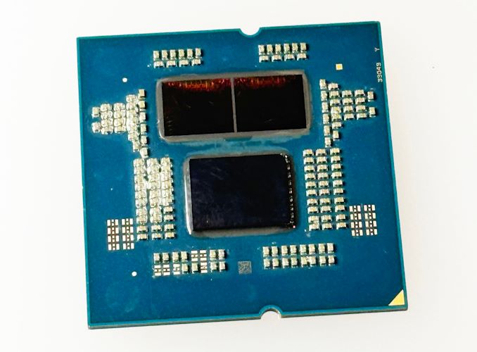
In what started last year as a handful of reports about instability with Intel's Raptor Lake desktop chips has, over the last several months, grown into a much larger saga. Facing their biggest client chip instability impediment in decades, Intel has been under increasing pressure to figure out the root cause of the issue and fix it, as claims of damaged chips have stacked up and rumors have swirled amidst the silence from Intel. But, at long last, it looks like Intel's latest saga is about to reach its end, as today the company has announced that they've found the cause of the issue, and will be rolling out a microcode fix next month to resolve it.

Officially, Intel has been working to identify the cause of desktop Raptor Lake’s instability issues since at least February of this year, if not sooner. In the interim they have discovered a couple of correlating factors – telling motherboard vendors to stop using ridiculous power settings for their out-of-the-box configurations, and finding a voltage-related bug in Enhanced Thermal Velocity Boost (eTVB) – but neither factor was the smoking gun that set all of this into motion. All of which had left Intel to continue searching for the root cause in private, and lots of awkward silence to fill the gaps in the public.

But it looks like Intel’s search has finally come to an end – even if Intel isn’t putting the smoking gun on public display quite yet. According to a fresh update posted to the company’s community website, Intel has determined the root cause at last, and has a fix in the works.

Per the company’s announcement, Intel has tracked down the cause of the instability issue to “elevated operating voltages”, that at its heart, stems from a flawed algorithm in Intel’s microcode that requested the wrong voltage. Consequently, Intel will be able to resolve the issue through a new microcode update, which pending validation, is expected to be released in the middle of August.

Based on extensive analysis of Intel Core 13th/14th Gen desktop processors returned to us due to instability issues, we have determined that elevated operating voltage is causing instability issues in some 13th/14th Gen desktop processors. Our analysis of returned processors confirms that the elevated operating voltage is stemming from a microcode algorithm resulting in incorrect voltage requests to the processor.

Intel is delivering a microcode patch which addresses the root cause of exposure to elevated voltages. We are continuing validation to ensure that scenarios of instability reported to Intel regarding its Core 13th/14th Gen desktop processors are addressed. Intel is currently targeting mid-August for patch release to partners following full validation.

Intel is committed to making this right with our customers, and we continue asking any customers currently experiencing instability issues on their Intel Core 13th/14th Gen desktop processors reach out to Intel Customer Support for further assistance.
-Intel Community Post

And while there’s nothing good for Intel about Raptor Lake’s instability issues or the need to fix them, that the problem can be ascribed to (or at least fixed by) microcode is about the best possible outcome the company could hope for. Across the full spectrum of potential causes, microcode is the easiest to fix at scale – microcode updates are already distributed through OS updates, and all chips of a given stepping (millions in all) run the same microcode. Even a motherboard BIOS-related issue would be much harder to fix given the vast number of different boards out there, never mind a true hardware flaw that would require Intel to replace even more chips than they already have.

Still, we’d also be remiss if we didn’t note that microcode is regularly used to paper over issues further down in the processor, as we’ve most famously seen with the Meltdown/Spectre fixes several years ago. So while Intel is publicly attributing the issue to microcode bugs, there are several more layers to the onion that is modern CPUs that could be playing a part. In that respect, a microcode fix grants the least amount of insight into the bug and the performance implications about its fix, since microcode can be used to mitigate so many different issues.

But for now, Intel’s focus is on communicating that they have fix and establishing a timeline for distributing it. The matter has certainly caused them a lot of consternation over the last year, and it will continue to do so for at least another month.

In the meantime, we’ve reached out to our Intel contacts to see if the company will be publishing additional details about the voltage bug and its fix. “Elevated operating voltages” is not a very satisfying answer on its own, and given the unprecedented nature of the issue, we’re hoping that Intel will be able to share additional details as to what’s going on, and how Intel will be preventing it in the future.

Intel Also Confirms a Via Oxidation Manufacturing Issue Affected Early Raptor Lake Chips

Tangential to this news, Intel has also made a couple of other statements regarding chip instability to the press and public over the last 48 hours that also warrant some attention.

First and foremost, leading up to Intel’s official root cause analysis of the desktop Raptor Lake instability issues, one possibility that couldn’t be written off at the time was that the root cause of the issue was a hardware flaw of some kind. And while the answer to that turned out to be “no,” there is a rather important “but” in there, as well.

As it turns out, Intel did have an early manufacturing flaw in the enhanced version of the Intel 7 process node used to build Raptor Lake. According to a post made by Intel to Reddit this afternoon, a “via Oxidation manufacturing issue” was addressed in 2023. However, despite the suspicious timing, according to Intel this is separate from the microcode issue driving instability issues with Raptor Lake desktop processors up to today.

Short answer: We can confirm there was a via Oxidation manufacturing issue (addressed back in 2023) but it is not related to the instability issue.

Long answer: We can confirm that the via Oxidation manufacturing issue affected some early Intel Core 13th Gen desktop processors. However, the issue was root caused and addressed with manufacturing improvements and screens in 2023. We have also looked at it from the instability reports on Intel Core 13th Gen desktop processors and the analysis to-date has determined that only a small number of instability reports can be connected to the manufacturing issue.

For the Instability issue, we are delivering a microcode patch which addresses exposure to elevated voltages which is a key element of the Instability issue. We are currently validating the microcode patch to ensure the instability issues for 13th/14th Gen are addressed.
-Intel Reddit Post

Ultimately, Intel says that they caught the issue early-on, and that only a small number of Raptor Lake were affected by the via oxidation manufacturing flaw. Which is hardly going to come as a comfort to Raptor Lake owners who are already worried about the instability issue, but if nothing else, it’s helpful that the issue is being publicly documented. Typically, these sorts of early teething issues go unmentioned, as even in the best of scenarios, some chips inevitably fail prematurely.

Unfortunately, Intel’s revelation here doesn’t offer any further details on what the issue is, or how it manifests itself beyond further instability. Though at the end of the day, as with the microcode voltage issue, the fix for any affected chips will be to RMA them with Intel to get a replacement.

Laptops Not Affected by Raptor Lake Microcode Issue

Finally, ahead of the previous two statements, Intel also released a statement to Digital Trends and a few other tech websites over the weekend, in response to accusations that Intel’s 13th generation Core mobile CPUs were also impacted by what we now know to be the microcode flaw. In the statement, Intel refuted those claims, stating that laptop chips were not suffering from the same instability issue.

Intel is aware of a small number of instability reports on Intel Core 13th/14th Gen mobile processors. Based on our in-depth analysis of the reported Intel Core 13th/14th Gen desktop processor instability issues, Intel has determined that mobile products are not exposed to the same issue. The symptoms being reported on 13th/14th Gen mobile systems – including system hangs and crashes – are common symptoms stemming from a broad range of potential software and hardware issues. As always, if users are experiencing issues with their Intel-powered laptops we encourage them to reach out to the system manufacturer for further assistance.
-Intel Rep to Digital Trends

Instead, Intel attributed any laptop instability issues to typical hardware and software issues – essentially claiming that they weren’t experiencing elevated instability issues. Whether this statement accounts for the via oxidation manufacturing issue is unclear (in large part because not all 13th Gen Core Mobile parts are Raptor Lake), but this is consistent with Intel’s statements from earlier this year, which have always explicitly cited the instability issues as desktop issues.

Tenstorrent Launches Wormhole AI Processors: 466 FP8 TFLOPS at 300W

Tenstorrent has unveiled its next-generation Wormhole processor for AI workloads that promises to offer decent performance at a low price. The company currently offers two add-on PCIe cards carrying one or two Wormhole processors as well as TT-LoudBox, and TT-QuietBox workstations aimed at software developers. The whole of today's release is aimed at developers rather than those who will deploy the Wormhole boards for their commercial workloads.

It is always rewarding to get more of our products into developer hands. Releasing development systems with our Wormhole™ card helps developers scale up and work on multi-chip AI software.” said Jim Keller, CEO of Tenstorrent. “In addition to this launch, we are excited that the tape-out and power-on for our second generation, Blackhole, is going very well.

Each Wormhole processor packs 72 Tensix cores (featuring five RISC-V cores supporting various data formats) with 108 MB of SRAM to deliver 262 FP8 TFLOPS at 1 GHz at 160W thermal design power. A single-chip Wormhole n150 card carries 12 GB of GDDR6 memory featuring a 288 GB/s bandwidth.

Wormhole processors offer flexible scalability to meet the varying needs of workloads. In a standard workstation setup with four Wormhole n300 cards, the processors can merge to function as a single unit, appearing as a unified, extensive network of Tensix cores to the software. This configuration allows the accelerators to either work on the same workload, be divided among four developers or run up to eight distinct AI models simultaneously. A crucial feature of this scalability is that it operates natively without the need for virtualization. In data center environments, Wormhole processors will scale both inside one machine using PCIe or outside of a single machine using Ethernet. 

From performance standpoint, Tenstorrent's single-chip Wormhole n150 card (72 Tensix cores at 1 GHz, 108 MB SRAM, 12 GB GDDR6 at 288 GB/s) is capable of 262 FP8 TFLOPS at 160W, whereas the dual-chip Wormhole n300 board (128 Tensix cores at 1 GHz, 192 MB SRAM, aggregated 24 GB GDDR6 at 576 GB/s) can offer up to 466 FP8 TFLOPS at 300W (according to Tom's Hardware).

To put that 466 FP8 TFLOPS at 300W number into context, let's compare it to what AI market leader Nvidia has to offer at this thermal design power. Nvidia's A100 does not support FP8, but it does support INT8 and its peak performance is 624 TOPS (1,248 TOPS with sparsity). By contrast, Nvidia's H100 supports FP8 and its peak performance is massive 1,670 TFLOPS (3,341 TFLOPS with sparsity) at 300W, which is a big difference from Tenstorrent's Wormhole n300. 

There is a big catch though. Tenstorrent's Wormhole n150 is offered for $999, whereas n300 is available for $1,399. By contrast, one Nvidia H100 card can retail for $30,000, depending on quantities. Of course, we do not know whether four or eight Wormhole processors can indeed deliver the performance of a single H300, though they will do so at 600W or 1200W TDP, respectively.

In addition to cards, Tenstorrent offers developers pre-built workstations with four n300 cards inside the less expensive Xeon-based TT-LoudBox with active cooling and a premium EPYC-powered TT-QuietBox with liquid cooling.

Sources: TenstorrentTom's Hardware

TSMCs Q2'24 Results: Best Quarter Ever as HPC Revenue Share Exceeds 52% on AI Demand

Taiwan Semiconductor Manufacturing Co. this week said its revenue for the second quarter 2024 reached $20.82 billion, making it the company's best quarter (at least in dollars) to date. TSMC's high-performance computing (HPC) platform revenue share exceeded 52% for the first time in many years due to demand for AI processors and rebound of the PC market.

TSMC earned $20.82 billion USD in revenue for the second quarter of 2024, a 32.8% year-over-year increase and a 10.3% increase from the previous quarter. Perhaps more remarkable, $20.82 billion is a higher result than the company posted Q3 2022 ($20.23 billion), the foundry's best quarter to date. Otherwise, in terms of profitability, TSMC booked $7.59 billion in net income for the quarter, for a gross margin of 53.2%. This is a decent bit off of TSMC's record margin of 60.4% (Q3'22), and comes as the company is still in the process of further ramping its N3 (3nm-class) fab lines.

When it comes to wafer revenue share, the company's N3 process technologies (3nm-class) accounted for 15% of wafer revenue in Q2 (up from 9% in the previous quarter), N5 production nodes (4nm and 5nm-classes) commanded 35% of TSMC's earnings in the second quarter (down from 37% in Q1 2024), and N7 fabrication processes (6nm and 7nm-classes) accounted for 17% of the foundry's wafer revenue in the second quarter of 2024 (down from 19% in Q1 2024). Advanced technologies all together (N3, N5, N7) accounted for 67% of total wafer revenue.

"Our business in the second quarter was supported by strong demand for our industry-leading 3nm and 5nm technologies, partially offset by continued smartphone seasonality," said Wendell Huang, Senior VP and Chief Financial Officer of TSMC. "Moving into third quarter 2024, we expect our business to be supported by strong smartphone and AI-related demand for our leading-edge process technologies."

TSMC usually starts ramping up production for Apple's fall products (e.g. iPhone) in the second quarter of the year, so it is not surprising that revenue share of N3 increased in Q2 of this year. Yet, keeping in mind that TSMC's revenue in general increased by 10.3% QoQ, the company's shipments of processors made on N5 and N7 nodes are showing resilience as demand for AI and HPC processors is high across the industry.

Speaking of TSMC's HPC sales, HPC platform sales accounted for 52% of TSMC's revenue for the first time in many years. The world's largest contract maker of chips produces many types of chips that get placed under the HPC umbrella, including AI processors, CPUs for client PCs, and system-on-chips (SoCs) for consoles, just to name a few. Yet, in this case TSMC attributes demand for AI processors as the main driver for its HPC success. 

As for smartphone platform revenue, its share dropped to 33% as actual sales declined by 1% quarter-over-quarter. All other segments grew by 5% to 20%.

For the third quarter of 2024, TSMC expects revenue between US$22.4 billion and US$23.2 billion, with a gross profit margin of 53.5% to 55.5% and an operating profit margin of 42.5% to 44.5%. The company's sales are projected to be driven by strong demand for leading-edge process technologies as well as increased demand for AI and smartphones-related applications.

The Corsair RM750e ATX 3.1 Review: Simple And Effective

As mainstream power supplies continue to make their subtle shift to the ATX 3.1 standard, the pace of change is picking up. Already most vendors offer at least one ATX 3.1 unit in their lineups, and thanks to the relatively small set of changes that come with the revised standard, PSU vendors have largely been able to tweak their existing ATX 3.0 designs, allowing for them to quickly roll-out updated power supplies. This means that the inflection point for ATX 3.1 as a whole is quickly approaching, as more and more designs get their update and make their way out to retail shelves.

Today we're looking at our first ATX 3.1-compliant PSU from Corsair, one of the industry's most prolific (and highest profile) power supply vendors. Their revised RMe line of power supplies are aimed at the mainstream gaming market, which is perhaps not too surprising given how important ATX 3.1 support and safety are to video cards. The RM750e model we're looking at today is the smallest capacity for the lineup, which stretches from 750 Watts up to a hefty 1200 Watts.

Overall, the RM750e is built to meet the demands of contemporary gaming systems, and boasts a great balance between features, performance, and cost. It is an 80Plus Gold certified unit with modular cables and PCIe 5.1/ATX 3.1 certified, offering a single 600W 12V-2x6 connector. We will explore its specifications, construction, and performance to determine its standing in today’s market.

Best CPUs for Gaming: July 2024

As the second quarter of 2024 is soon set to unfold, there are many things to be excited about, especially as Computex 2024 has been and gone. We now know that AMD's upcoming Ryzen 9000 series desktop processors using the new Zen 5 cores will be hitting shelves at the end of the month (31st July), and on top of this, AMD also recently slashed pricing on their Zen 4 (Ryzen 8000) processors. Intel still needs to follow suit with their 14th or 13th Gen Core series processors, but right now from a cost standpoint, AMD is in a much better position.

Since the publication of our last guide, the only notable CPU to be launched was Intel's special binned Core i9-14900KS, which not only pushes clock speeds up to 6.2 GHz but is the last processor to feature Intel's iconic Core I series nomenclature. The other big news in the CPU world was from Intel, with a statement issued about pushing users to use the Intel Default Specification on Intel's 14th and 13th Gen processors, which ultimately limits the performance compared to published data. We're still in the process of 

While the CPU market has been relatively quiet so far this year, and things are set to pick up once AMD's Zen 5 and Intel's Arrow Lake desktop chips are all launched onto the market, it means today we are working for the same hymn sheet as our previous guide. With AMD's price drops on Ryzen 7000 series processors, much of the guide reflects this as AMD and Intel's performance is neck and neck in many use cases, but cost certainly plays a big factor in selecting a new CPU. As we move into the rest of 2024, the CPU market looks set to see the rise of the 'AI PC,' which is looking set to be something that many companies will focus on by the end of 2024, both on mobile and desktop platforms.

Crucial P310 NVMe SSD Unveiled: Micron's Play in the M.2 2230 Market

Hand-held gaming consoles based on notebook platforms (such as the Valve SteamDeck, ASUS ROG Ally, and the MSI Claw) are one of the fastest growing segments in the PC gaming market. The form-factor of such systems has created a demand for M.2 2230 NVMe SSDs. Almost all vendors have a play in this market, and even Micron has OEM SSDs (such as the Micron 2400, 2550, and 2500 series) in this form-factor. Crucial has strangely not had an offering with its own brand name to target this segment, but that changes today with the launch of the Crucial P310 NVMe SSD.

The Crucial P310 is a family of M.2 2230 PCIe Gen4 NVMe SSDs boasting class-leading read/write speeds of 7.1 GBps and 6 GBps. The family currently has two capacity points - 1 TB and 2 TB. Micron claims that the use of its 232L 3D NAND and Phison's latest E27T DRAM-less controller (fabricated in TSMC's 12nm process) help in reducing power consumption under active use compared to the competition - directly translating to better battery life for the primary use-case involving gaming handheld consoles.

Based on the specifications, it appears that the drives are using 232L 3D QLC. Compared to the recently-released Micron 2550 SSD series in the same form-factor, a swap in the controller has enabled some improvements in both power efficiency and performance. The other specifications are summarized in the table below.

Crucial P310 SSD Specifications
Capacity 2 TB 1 TB
Controller Phison E27T (DRAM-less)
NAND Flash Micron 232L 3D QLC NAND
Form-Factor, Interface Single-Sided M.2-2230
PCIe 4.0 x4, NVMe
Sequential Read 7100 MB/s
Sequential Write 6000 MB/s
Random Read IOPS 1 M
Random Write IOPS 1.2 M
SLC Caching Yes
TCG Pyrite Encryption Yes
Warranty 5 Years
Write Endurance 440 TBW
0.12 DWPD
220 TBW
0.12 DWPD
MSRP $215 $115

The power efficiency, cost, and capacity points are plus points for the Crucial P310 family. However, the endurance ratings are quite low. Gaming workloads are inherently read-heavy, and this may not be a concern for the average consumer. However, a 0.12 DWPD rating may turn out to be a negative aspect when compared against the competition's 0.33 DWPD offerings in the same segment.

Samsung Validates LPDDR5X Running at 10.7 GT/sec with MediaTek's Dimensity 9400 SoC

Samsung has successfully validated its new LPDDR5X-10700 memory with MediaTek's upcoming Dimensity platform. At present, 10.7 GT/s is the highest performing speed grade of LPDDR5X DRAM slated to be released this year, so the upcoming Dimensity 9400 system-on-chip will get the highest memory bandwidth available for a mobile application processor.

The verification process involved Samsung's 16 GB LPDDR5X package and MediaTek's soon-to-be-announced Dimensity 9400 SoC for high-end 5G smartphones. Usage of LPDDR5X-10700 provides a memory bandwidth of 85.6 GB/second over a 64-bit interface, which will be available for bandwidth-hungry applications like graphics and generative AI.

"Working together with Samsung Electronics has made it possible for MediaTek's next-generation Dimensity chipset to become the world's first to be validated at LPDDR5X operating speeds up to 10.7Gbps, enabling upcoming devices to deliver AI functionality and mobile performance at a level we have never seen before," said JC Hsu, Corporate Senior Vice President at MediaTek. "This updated architecture will make it easier for developers and users to leverage more AI capabilities and take advantage of more features with less impact on battery life."

Samsung's LPDDR5X 10.7 GT/s memory in made on the company's 12nm-class DRAM process technology and is said to provide a more than 25% improvement in power efficiency over previous-generation LPDDR5X, in addition to extra performance. This will positively affect improved user experience, including enhanced on-device AI capabilities, such as faster voice-to-text conversion, and better quality graphics.

Overall, the two companies completed this process in just three months. Though it remains to be seen when smartphones based on the Dimensity 9400 application processor and LPDDR5X memory are set to be available on the market, as MediaTek has not yet even formally announced the SoC itself.

"Through our strategic cooperation with MediaTek, Samsung has verified the industry's fastest LPDDR5X DRAM that is poised to lead the AI smartphone market," said YongCheol Bae, Executive Vice President of Memory Product Planning at Samsung Electronics. "Samsung will continue to innovate through active collaboration with customers and provide optimum solutions for the on-device AI era."

Western Digital Adds 8TB Model to Popular High-End SN850X SSD Drive Family

Western Digital has quietly introduced an 8 TB version of its high-end SN850X SSD, doubling the top capacity of the well-regarded drive family. The new drive offers performance on par with other members of the range, but with twice as much capacity as the previous top-end model – and with a sizable price premium to go with its newfound capacity.

Western Digital introduced its WD_Black SN850X SSDs in the summer of 2022, releasing single-sided 1 TB and 2 TB models, along with a double-sided 4 TB model. But now almost two years down the line, the company has seen it fit to introduce the even higher capacity 8 TB model to serve as their flagship PCIe 4.0 SSD, and keep with the times of NAND prices and SSD capacity demands.

Like the other SN850X models, WD is using their in-house, 8-channel controller for the new 8 TB model, which sports a PCIe 4.0 x4 interface. And being that this is a high-end SSD, the controller is paired with DRAM (DDR4) for page index caching, though WD doesn't disclose how much DRAM is on any given model. On the NAND front, WD is apparently still using their BiCS 5 112L NAND here, which means we're looking at 4x 2 TB NAND chips, each with 16 1Tbit TLC dies on-board, twice as many dies as were used on the NAND chips for the 4 TB model.

The peak read speed of the new 8TB model is 7,200 MB/sec, which is actually a smidge below the performance the 4 TB and 2 TB models due to the overhead from the additional NAND dies. Meanwhile peak sequential write speeds remain at 6,600 MB/sec, while 4K random write performance maxes out at 1200K IOPS for both reads and writes. It goes without saying that this is a step below the performance of the market flagship PCIe 5.0 SSDs available today, but it's going to be a bit longer until anyone else besides Phison is shipping a PCIe 5.0 controller – never mind the fact that these drives aren't available in 8 TB capacities.

The 8 TB SN850X also keeps the same drive endurance progression as the rest of the SN850X family. In this case, double the NAND brings double the endurance of the 4 TB model, for an overall endurance of 4800 terabytes written (TBW). Or in terms of drive writes per day, this is the same 0.33 rating as the other SN850X drives.

WD_Back SN850X SSD Specifications
Capacity 8 TB 4 TB 2 TB 1 TB
Controller WD In-House: 8 Channel, DRAM (DDR4)
NAND Flash WD BiCS 5 TLC
Form-Factor, Interface Double-Sided M.2-2280
PCIe 4.0 x4, NVMe
Single-Sided M.2-2280
PCIe 4.0 x4, NVMe
Sequential Read 7200 MB/s 7300 MB/s 7300 MB/s 7300 MB/s
Sequential Write 6600 MB/s 6600 MB/s 6600 MB/s 6300 MB/s
Random Read IOPS 1200K 1200K 1200K 800K
Random Write IOPS 1200K 1100K 1100K 1100K
SLC Caching Yes
TCG Opal Encryption 2.01
Warranty 5 Years
Write Endurance 4800 TBW
0.33 DWPD
2400 TBW
0.33 DWPD
1200 TBW
0.33 DWPD
600 TBW
0.33 DWPD
MSRP (No Heatsink) $850 $260 $140 $85

Western Digital's WD_Black SN850X is available both with and without aluminum heatsink. The version without a heatsink aimed at laptops and BYOC setups costs $849.99, whereas a version with an aluminum heat spreader comes at $899.99. In both cases the 8 TB drive carries a significant price premium over the existing 4 TB model, which is readily available for $259.99.

This kind of price premium is unfortunately typical for 8 TB drives, and will likely remain so until both supply and demand for the high-capacity drives picks up to bring prices down. Still, with rival drives such as Corsair's MP600 Pro XT 8 TB and Sabrent's Rocket 4 Plus 8 TB going for $965.99 and $1,199.90 respectively, the introduction of the 8 TB SN850X is definitely pushing high-capacity M.2 SSD prices down, albeit slowly. So for systems with multiple M.2 slots, at least, the sweet spot on drive pricing is still to get two 4 TB SSDs.

Micron Expands Datacenter DRAM Portfolio with MR-DIMMs

The compute market has always been hungry for memory bandwidth, particularly for high-performance applications in servers and datacenters. In recent years, the explosion in core counts per socket has further accentuated this need. Despite progress in DDR speeds, the available bandwidth per core has unfortunately not seen a corresponding scaling.

The stakeholders in the industry have been attempting to address this by building additional technology on top of existing widely-adopted memory standards. With DDR5, there are currently two technologies attempting to increase the peak bandwidth beyond the official speeds. In late 2022, SK hynix introduced MCR-DIMMs meant for operating with specific Intel server platforms. On the other hand, JEDEC - the standards-setting body - also developed specifications for MR-DIMMs with a similar approach. Both of them build upon existing DDR5 technologies by attempting to combine multiple ranks to improve peak bandwidth and latency.

How MR-DIMMs Work

The MR-DIMM standard is conceptually simple - there are multiple ranks of memory modules operating at standard DDR5 speeds with a data buffer in front. The buffer operates at 2x the speed on the host interface side, allowing for essentially double the transfer rates. The challenges obviously lie in being able to operate the logic in the host memory controller at the higher speed and keeping the power consumption / thermals in check.

The first version of the JEDEC MR-DIMM standard specifies speeds of 8800 MT/s, with the next generation at 12800 MT/s. JEDEC also has a clear roadmap for this technology, keeping it in sync with the the improvements in the DDR5 standard.

Micron MR-DIMMs - Bandwidth and Capacity Plays

Micron and Intel have been working closely in the last few quarters to bring their former's first-generation MR-DIMM lineup to the market. Intel's Xeon 6 Family with P-Cores (Granite Rapids) is the first platform to bring MR-DIMM support at 8800 MT/s on the host side. Micron's standard-sized MR-DIMMs (suitable for 1U servers) and TFF (tall form-factor) MR-DIMMs (for 2U+ servers) have been qualified for use with the same.

The benefits offered by MR-DIMMs are evident from the JEDEC specifications, allowing for increased data rates and system bandwidth, with improvements in latency. On the capacity side, allowing for additional ranks on the modules has enabled Micron to offer a 256 GB capacity point. It must be noted that some vendors are also using TSV (through-silicon vias) technology to to increase the per-package capacity at standard DDR5 speeds, but this adds additional cost and complexity that are largely absent in the MR-DIMM manufacturing process.

The tall form-factor (TFF) MR-DIMMs have a larger surface area compared to the standard-sized ones. For the same airflow configuration, this allows the DIMM to have a better thermal profile. This provides benefits for energy efficiency as well by reducing the possibility of thermal throttling.

Micron is launching a comprehensive lineup of MR-DIMMs in both standard and tall form-factors today, with multiple DRAM densities and speed options as noted above.

MRDIMM Benefits - Intel Granite Rapids Gets a Performance Boost

Micron and Intel hosted a media / analyst briefing recently to demonstrate the benefits of MR-DIMMs for Xeon 6 with P-Cores (Granite Rapids). Using a 2P configuration with 96-core Xeon 6 processors, benchmarks for different workloads were processed with both 8800 MT/s MR-DIMMs and 6400 MT/s RDIMMs. The chosen workloads are particularly notorious for being limited in performance by memory bandwidth.

OpenFOAM is a widely-used CFD workload that benefits from MR-DIMMs. For the same memory capacity, the 8800 MT/s MR-DIMM shows a 1.31x speedup based on higher average bandwidth and IPC improvements, along with lower last-level cache miss latency.

The performance benefits are particularly evident with more cores participating the workload.

Apache Spark is a commonly used big-data platform operating on large datasets. Depending on the exact dataset in the picture, the performance benefits of MR-DIMMs can vary. Micron and Intel used a 2.4TB set from Intel's Hibench benchmark suite for this benchmark, showing a 1.2x speedup at the same capacity and 1.7x speedup with doubled-capacity TFF MR-DIMMs.

Avoiding the need to push data back to the permanent storage also contributes to the speedup.

The higher speed offered by MR-DIMMs also helps in AI inferencing workloads, with Micron and Intel showing a 1.31x inference performance improvement along with reduced time to first token for a Llama 3 8B parameter model. Obviously, purpose-built inferencing solutions based on accelerators will perform better. However, this was offered as a demonstration of the type of CPU workloads that can benefit from MR-DIMMs.

As the adage goes, there is no free lunch. At 8800 MT/s, MR-DIMMs are definitely going to guzzle more power compared to 6400 MT/s RDIMMs. However, the faster completion of workloads mean that the the energy consumption for a given workload will be lower for the MR-DIMM configurations. We would have liked Micron and Intel to quantify this aspect for the benchmarks presented in the demonstration. Additionally, Micron indicated that the energy efficiency (in terms of pico-joules per bit transferred) is largely similar for both the 6400 MT/s RDIMMs and 8800 MT/s MR-DIMMs.

Key Takeaways

The standardization of MR-DIMMs by JEDEC allows multiple industry stakeholders to participate in the market. Customers are not vendor-locked and can compare and contrast options from different vendors to choose the best fit for their needs.

At Computex, we saw MR-DIMMs from ADATA on display. As a Tier-2 vendor without its own DRAM fab, ADATA's play is on cost benefits with the possibility of the DRAM die being sourced from different fabs. The MR-DIMM board layout is dictated by JEDEC specifications, and this allows Tier-2 vendors to have their own play with pricing flexibility. Modules are also built based on customer orders. Micron, on the other hand, has a more comprehensive portfolio / lineup of SKUs for different use-cases with the pros and cons of vertical integration in the picture.

Micron is also not the first to publicly announce MR-DIMM sampling. Samsung announced their own lineup (based on 16Gb DRAM dies) last month. It must be noted that Micron's MR-DIMM portfolio uses 16 Gb, 24 Gb, and 32 Gb dies fabricated in 1β technology. While Samsung's process for the 16 Gb dies used in their MR-DIMMs is not known, Micron believes that their MR-DIMM technology will provide better power efficiency compared to the competition while also offering customers a wider range of capacities and configurations.

The AMD Zen 5 Microarchitecture: Powering Ryzen AI 300 Series For Mobile and Ryzen 9000 for Desktop

Back at Computex 2024, AMD unveiled their highly anticipated Zen 5 CPU microarchitecture during AMD CEO Dr. Lisa Su's opening keynote. AMD announced not one but two new client platforms that will utilize the latest Zen 5 cores. This includes AMD's latest AI PC-focused chip family for the laptop market, the Ryzen AI 300 series. In comparison, the Ryzen 9000 series caters to the desktop market, which uses the preexisting AM5 platform.

Built around the new Zen 5 CPU microarchitecture with some fundamental improvements to both graphics and AI performance, the Ryzen AI 300 series, code-named Strix Point, is set to deliver improvements in several areas. The Ryzen AI 300 series looks set to add another footnote in the march towards the AI PC with its mobile SoC featuring a new XDNA 2 NPU, from which AMD promises 50 TOPS of performance. AMD has also upgraded the integrated graphics with the RDNA 3.5, which is designed to replace the last generation of RDNA 3 mobile graphics, for better performance in games than we've seen before.

Further to this, during AMD's recent Tech Day last week, AMD disclosed some of the technical details regarding Zen 5, which also covers a number of key elements under the hood on both the Ryzen AI 300 and the Ryzen 9000 series. On paper, the Zen 5 architecture looks quite a big step up compared to Zen 4, with the key component driving Zen 5 forward through higher instructions per cycle than its predecessor, which is something AMD has managed to do consistently from Zen to Zen 2, Zen 3, Zen 4, and now Zen 5.

Troubled AI Processor Developer Graphcore Finds a Buyer: SoftBank

After months of searching for a buyer, troubled U.K.-based AI processor designer Graphcore said on Friday that it has been acquired by SoftBank. The company will operate as a wholly owned subsidiary of SoftBank and will possibly collaborate with Arm, but what remains to be seen what happens to the unique architecture of Graphcore's intelligence processing units (IPUs).

Graphcore will retain its name as it will become a wholly owned subsidiary of SoftBank, which paid either $400 million (according to EE Times) or $500 million (according to BBC) for the company. Over its lifetime, Graphcore has received a total of $700 million of investments from Microsoft and Sequoia Capital, and at its peak in late 2020, was valued at $2.8 billion. Nigel Toon will remain at the helm of Graphcore, which will hire new staff in its UK offices and continue to be headquartered in Bristol, with additional offices in Cambridge, London, Gdansk (Poland), and Hsinchu (China).

"This is a tremendous endorsement of our team and their ability to build truly transformative AI technologies at scale, as well as a great outcome for our company," said Nigel Toon. "Demand for AI compute is vast and continues to grow. There remains much to do to improve efficiency, resilience, and computational power to unlock the full potential of AI. In SoftBank, we have a partner that can enable the Graphcore team to redefine the landscape for AI technology."

Although Graphcore says that it had won contracts with major high-tech companies and deployed its IPUs, it could not compete against NVIDIA and other prêt-à-porter AI processor vendors due to insufficient funding. In the recent years the company's problems were so severe that it had to lay off 20% of its staff, bringing its headcount to around 500. Those cuts also saw office closures in Norway, Japan, and South Korea, which made it even harder to compete against big players.

Graphcore certainly hopes that with SoftBank's deep pockets and willingness to invest in AI technologies in general and AI processors in particular, it will finally be able to compete head-to-head with established players like NVIDIA.

When asked whether Graphcore will work with SoftBank's Arm, Nigel Toon said that he was looking forward to work with all companies controlled by its parent, including Arm. Meanwhile, SoftBank itself is reportedly looking forward to build its own AI processor venture called Project Izanagi to compete against NVIDIA, whereas Arm is reportedly developing AI processors that will work in datacenters owned by SoftBank. Therefore, it remains to be seen where does Graphcore fit in.

For now, the best processor that Graphcore has is its Colossus MK2 IPU, which is built using 59.4 billion transistors and packs in 1,472 independent cores with simultaneous multithreading (SMT) capable of handling 8,832 parallel threads. Instead of using HBM or other types of external memory, the chip integrates 900 MB of SRAM, providing an aggregated bandwidth of 47.5 TB/s per chip. Additionally, it features 10 IPU links to scale with other MK2 processors. When it comes to performance, the MK2 C600 delivers 560 TFLOPS FP8, 280 TFLOPS FP16, and 70 TFLOPS of FP32 performance at 185W. To put the numbers into context, NVIDIA's A100 delivers 312 FP16 TFLOPS without sparsity as well as 19.5 FP32 TFLOPS, whereas NVIDIA's H100 card offers 3,341 FP8 TFLOPS.

Sources: GraphcoreEE TimesBBCReuters

Applied Materials' New Deposition Tool Enables Copper Wires to Be Used for 2nm and Beyond

Although the pace of Moore's Law has undeniably slackened in the last decade, transistor density is still increasing with every new process technology. But there is a challenge with feeding power to smaller transistors, as with the smaller transistors comes thinner power wires within the chip, which increases their resistance and may cause yield loss. Looking to combat that effect, this week Applied Materials introduced its new Applied Endura Copper Barrier Seed IMS with Volta Ruthenium Copper Vapor Deposition (CVD) tool, which enables chipmakers to keep using copper for wiring with 2 nm-class and more advanced process technologies.

Today's advanced logic processors have about 20 layers of metal, with thin signal wires and thicker power wires. Scaling down wiring with shrinking transistors presents numerous challenges. Thinner wires have higher electrical resistance, while closer wires heighten capacitance and electrical crosstalk. The combination of the two can lead to increased power consumption while also limiting performance scaling, which is particularly problematic for datacenter grade processors that are looking to have it all. Moving power rails to a wafer's back-side is expected to enhance performance and efficiency by reducing wiring complexity and freeing up space for more transistors. 

But backside power delivery network (BSPDN) does not solve the problem with thin wires in general. As lithographic scaling progresses, both transistor features and wiring trenches become smaller. This reduction means that barriers and liners take up more space in these trenches, leaving insufficient room to deposit copper without creating voids, which raises resistance and can lower yields. Additionally, the closer proximity of wires thins the low-k dielectrics, making them more vulnerable to damage during the etching process. This damage increases capacitance and weakens the chips, making them unsuitable for 3D stacking. Consequently, as the industry advances, copper wiring faces significant physical scaling challenges. But Applied Materials has a solution.

Adopting Binary RuCo Liners

Contemporary manufacturing technologies use reflow to fill interconnects with copper, where anneals help the copper flow from the wafer surface into wiring trenches and vias. This process depends on the liners on which the copper flows. Normally, a CVD cobalt film was used for liners, but this film is too thick for 3nm-class nodes (which would affect resistance and yield).

Applied Materials proposes using a ruthenium cobalt (RuCo) binary liner with a thickness under 20A (2nm, 20 angstroms), which would provide better surface properties for copper reflow. This would ultimately allow for 33% more space for void-free conductive copper to be reflowed, reducing the overall resistance by 25%. While usage of the new liner requires new tooling, it can enable better interconnects that mean higher performance, lower power consumption and higher yields.

Applied Materials says that so far its new Endura Copper Barrier Seed IMS with Volta Ruthenium CVD tool has been adopted by all leading logic makers, including TSMC and Samsung Foundry for their 3nm-class nodes and beyond.

"The semiconductor industry must deliver dramatic improvements in energy-efficient performance to enable sustainable growth in AI computing," said Dr. Y.J. Mii, Executive Vice President and Co-Chief Operating Officer at TSMC. "New materials that reduce interconnect resistance will play an important role in the semiconductor industry, alongside other innovations to improve overall system performance and power."

New Low-K Dielectric

But thin and efficient liner is not the only thing crucial for wiring at 3nm production nodes and beyond. Trenches for wiring are filed not only with a Co/RuCo liner and a Ta/N barrier, but with low dielectric constant (Low-K) film to minimize electrical charge buildup, reduce power consumption, and lower signal interference. Applied Materials has offered its Black Diamond Low-K film since the early 2000s. 

But new production nodes require better dielectrics, so this week the company introduced an upgraded version of Black Diamond material and a plasma-enhanced chemical vapor deposition (PEVCD) tool to apply it, the Producer Black Diamond PECVD series. This new material allows for scaling down to 2nm and beyond by further reducing the dielectric constant while also increasing the mechanical strength of the chips, which is good for 3D stacking both for logic and memory. The new Black Diamond is being rapidly adopted by major logic and DRAM chipmakers, Applied says.

"The AI era needs more energy-efficient computing, and chip wiring and stacking are critical to performance and power consumption," said Dr. Prabu Raja, President of the Semiconductor Products Group at Applied Materials. "Applied's newest integrated materials solution enables the industry to scale low-resistance copper wiring to the emerging angstrom nodes, while our latest low-k dielectric material simultaneously reduces capacitance and strengthens chips to take 3D stacking to new heights."

Sources: Applied Materials (12)

Samsung Joins The 60 TB SSD Club, Looking Forward To 120 TB Drives

Multiple companies offer high-capacity SSDs, but until recently, only one company offered high-performance 60 TB-class drives with a PCIe interface: Solidigm. As our colleagues from Blocks & Files discovered, Samsung quietly rolled out its BM1743 61.44 TB solid-state drive in mid-June and now envisions 120 TB-class SSDs based on the same platform.

Samsung's BM1743 61.44 TB features a proprietary controller and relies on Samsung's 7th Generation V-NAND (3D NAND) QLC memory. Moreover, Samsung believes that its 7th Gen V-NAND 'has the potential to accommodate up to 122.88 TB,' 

Samsung plans to offer the BM1743 in two form factors: U.2 for PCIe 4.0 x4 to address traditional servers and E3.S for PCIe 5.0 x4 interfaces to address machines designed to offer maximum storage density. BM1743 can address various applications, including AI training and inference, content delivery networks, and read-intensive workloads. To that end, its write endurance is 0.26 drive writes per day (DWPD) over five years.

Regarding performance, Samsung's BM1743 is hardly a champion compared to high-end drives for gaming machines and workstations. The drive can sustainably achieve sequential read speeds of 7,200 MB/s and write speeds of 2,000 MB/s. It can handle up to 1.6 million 4K random reads and 110,000 4K random writes for random operations.

Power consumption details for the BM1743 have not been disclosed, though it is expected to be high. Meanwhile, the drive's key selling point is its massive storage density, which likely outweighs concerns over its absolute power efficiency for intended applications, as a 60 TB SSD still consumes less than multiple storage devices offering similar capacity and performance.

As noted above, Samsung's BM1743 61.44 TB faces limited competition in the market, so its price will be quite high. For example, Solidigm's D5-P5336 61.44 TB SSD costs $6,905. Other companies, such as Kioxia, Micron, and SK Hynix, have not yet introduced their 60TB-class SSDs, which gives Samsung and Solidigm an edge for now.

UPDATE 7/25: We removed mention of Western Digital's 60 TB-class SSDs, as the company does not currently list any such drives on their website

Kioxia's High-Performance 3D QLC NAND Enables High-End High-Capacity SSDs

This week, Kioxia introduced its new 3D QLC NAND devices aimed at high-performance, high-capacity drives that could redefine what we typically expect from QLC-based SSDs. The components are 1 Tb and 2 Tb 3D QLC NAND ICs with a 3600 MT/s interface speed that could enable M.2-2230 SSDs with a 4 TB capacity and decent performance.

Kioxia's 1 Tb (128 MB) and 2 Tb (256 TB) 3D QLC NAND devices are made on the company's BICS 8 process technology and feature 238 active layers as well as CMOS directly Bonded to Array (CBA) design, which implies that CMOS (including interface and buffers circuitry) is built on a specialized node and bonded to the memory array. Such a manufacturing process enabled Kioxia (and its manufacturing partner Western Digital) to achieve a particularly high interface speed of 3600 MT/s.

In addition to being one of the industry's first 2 Tb QLC NAND devices, the component features a 70% higher write power efficiency compared to Kioxia's BICS 5 3D QLC NAND devices, which is a bit vague statement as the new ICs have higher capacity and performance in general. This feature will be valuable for data centre applications, though I do not expect someone to use 3D QLC memory for write-intensive applications in general. Yet, these devices will be just what the doctor ordered for AI: read-intensive, content distribution, and backup storage.

It is interesting to note that Kioxia's 1 Tb 3D QLC NAND, optimized for performance, has a 30% faster sequential write performance and a 15% lower read latency than the 2 Tb 3D QLC component. These qualities (alongside a 3600 MT/s interface) promise to make Kioxia's 1 Tb 3D QLC competitive even for higher-end PCIe Gen5 x4 SSDs, which currently exclusively use 3D TLC memory.

The remarkable storage density of Kioxia's 2Tb 3D QLC NAND devices will allow customers to create high-capacity SSDs in compact form factors. For instance, a 16-Hi stacked package (measuring 11.5 mm × 13.5 mm × 1.5 mm) can be used to build a 4TB M.2-2230 drive or a 16TB M.2-2280 drive. Even a single 16-Hi package could be enough to build a particularly fast client SSD.

Kioxia is now sampling its 2 Tb 3D QLC NAND BiCS 8 memory with customers, such as Pure Storage.

"We have a long-standing relationship with Kioxia and are delighted to incorporate their eighth-generation BiCS Flash 2Tb QLC flash memory products to enhance the performance and efficiency of our all-flash storage solutions," said Charles Giancarlo, CEO of Pure Storage. "Pure's unified all-flash data storage platform is able to meet the demanding needs of artificial intelligence as well as the aggressive costs of backup storage. Backed by Kioxia technology, Pure Storage will continue to offer unmatched performance, power efficiency, and reliability, delivering exceptional value to our customers."

"We are pleased to be shipping samples of our new 2Tb QLC with the new eighth-generation BiCS flash technology," said Hideshi Miyajima, CTO of Kioxia. "With its industry-leading high bit density, high speed data transfer, and superior power efficiency, the 2Tb QLC product will offer new value for rapidly emerging AI applications and large storage applications demanding power and space savings."

There is no word on when the 1 Tb 3D QLC BiCS 8 memory will be sampled or released to the market.

❌