Titanium alloys are essential structural materials for a wide variety of applications, from aerospace and energy infrastructure to biomedical equipment. But like most metals, optimizing their properties tends to involve a tradeoff between two key characteristics: strength and ductility. Stronger materials tend to be less deformable, and deformable materials tend to be mechanically weak.
Now, researchers at MIT, collaborating with researchers at ATI Specialty Materials, have discovered an approach for creating new titanium alloys that can exceed this historical tradeoff, leading to new alloys with exceptional combinations of strength and ductility, which might lead to new applications.
The findings are described in the journal Advanced Materials, in a paper by Shaolou Wei ScD ’22, Professor C. Cem Tasan, postdoc Kyung-Shik Kim, and John Foltz from ATI Inc. The improvements, the team says, arise from tailoring the chemical composition and the lattice structure of the alloy, while also adjusting the processing techniques used to produce the material at industrial scale.
Titanium alloys have been important because of their exceptional mechanical properties, corrosion resistance, and light weight when compared to steels for example. Through careful selection of the alloying elements and their relative proportions, and of the way the material is processed, “you can create various different structures, and this creates a big playground for you to get good property combinations, both for cryogenic and elevated temperatures,” Tasan says.
But that big assortment of possibilities in turn requires a way to guide the selections to produce a material that meets the specific needs of a particular application. The analysis and experimental results described in the new study provide that guidance.
The structure of titanium alloys, all the way down to atomic scale, governs their properties, Tasan explains. And in some titanium alloys, this structure is even more complex, made up of two different intermixed phases, known as the alpha and beta phases.
“The key strategy in this design approach is to take considerations of different scales,” he says. “One scale is the structure of individual crystal. For example, by choosing the alloying elements carefully, you can have a more ideal crystal structure of the alpha phase that enables particular deformation mechanisms. The other scale is the polycrystal scale, that involves interactions of the alpha and beta phases. So, the approach that’s followed here involves design considerations for both.”
In addition to choosing the right alloying materials and proportions, steps in the processing turned out to play an important role. A technique called cross-rolling is another key to achieving the exceptional combination of strength and ductility, the team found.
Working together with ATI researchers, the team tested a variety of alloys under a scanning electron microscope as they were being deformed, revealing details of how their microstructures respond to external mechanical load. They found that there was a particular set of parameters — of composition, proportions, and processing method — that yielded a structure where the alpha and beta phases shared the deformation uniformly, mitigating the cracking tendency that is likely to occur between the phases when they respond differently. “The phases deform in harmony,” Tasan says. This cooperative response to deformation can yield a superior material, they found.
“We looked at the structure of the material to understand these two phases and their morphologies, and we looked at their chemistries by carrying out local chemical analysis at the atomic scale. We adopted a wide variety of techniques to quantify various properties of the material across multiple length scales, says Tasan, who is the POSCO Professor of Materials Science and Engineering and an associate professor of metallurgy. “When we look at the overall properties” of the titanium alloys produced according to their system, “the properties are really much better than comparable alloys.”
This was industry-supported academic research aimed at proving design principles for alloys that can be commercially produced at scale, according to Tasan. “What we do in this collaboration is really toward a fundamental understanding of crystal plasticity,” he says. “We show that this design strategy is validated, and we show scientifically how it works,” he adds, noting that there remains significant room for further improvement.
As for potential applications of these findings, he says, “for any aerospace application where an improved combination of strength and ductility are useful, this kind of invention is providing new opportunities.”
The work was supported by ATI Specialty Rolled Products and used facilities of MIT.nano and the Center for Nanoscale Systems at Harvard University.
Metals get softer when they are heated, which is how blacksmiths can form iron into complex shapes by heating it red hot. And anyone who compares a copper wire with a steel coat hanger will quickly discern that copper is much more pliable than steel.
But scientists at MIT have discovered that when metal is struck by an object moving at a super high velocity, the opposite happens: The hotter the metal, the stronger it is. Under those conditions, which put extreme stress on the metal, copper can actually be just as strong as steel. The new discovery could lead to new approaches to designing materials for extreme environments, such as shields that protect spacecraft or hypersonic aircraft, or equipment for high-speed manufacturing processes.
The findings are described in a paper appearing today in the journal Nature, by Ian Dowding, an MIT graduate student, and Christopher Schuh, former head of MIT’s Department of Materials Science and Engineering, now dean of engineering at Northwestern University and visiting professor at MIT.
The new finding, the authors write, “is counterintuitive and at odds with decades of studies in less extreme conditions.” The unexpected results could affect a variety of applications because the extreme velocities involved in these impacts occur routinely in meteorite impacts on spacecraft in orbit and in high-speed machining operations used in manufacturing, sandblasting, and some additive manufacturing (3D printing) processes.
The experiments the researchers used to find this effect involved shooting tiny particles of sapphire, just millionths of a meter across, at flat sheets of metal. Propelled by laser beams, the particles reached high velocities, on the order of a few hundred meters per second. While other researchers have occasionally done experiments at similarly high velocities, they have tended to use larger impactors, at the scale of centimeters or larger. Because these larger impacts were dominated by effects of the shock of the impact, there was no way to separate out the mechanical and thermal effects.
The tiny particles in the new study don’t create a significant pressure wave when they hit the target. But it has taken a decade of research at MIT to develop methods of propelling such microscopic particles at such high velocities. “We’ve taken advantage of that,” Schuh says, along with other new techniques for observing the high-speed impact itself.
The team used extremely high-speed cameras “to watch the particles as they come in and as they fly away,” he says. As the particles bounce off the surface, the difference between the incoming and outgoing velocities “tells you how much energy was deposited” into the target, which is an indicator of the surface strength.
The tiny particles they used were made of alumina, or sapphire, and are “very hard,” Dowding says. At 10 to 20 microns (millionths of a meter) across, these are between one-tenth and one-fifth of the thickness of a human hair. When the launchpad behind those particles is hit by a laser beam, part of the material vaporizes, creating a jet of vapor that propels the particle in the opposite direction.
The researchers shot the particles at samples of copper, titanium, and gold, and they expect their results should apply to other metals as well. They say their data provide the first direct experimental evidence for this anomalous thermal effect of increased strength with greater heat, although hints of such an effect had been reported before.
The surprising effect appears to result from the way the orderly arrays of atoms that make up the crystalline structure of metals move under different conditions, according to the researchers’ analysis. They show that there are three separate effects governing how metal deforms under stress, and while two of these follow the predicted trajectory of increasing deformation at higher temperatures, it is the third effect, called drag strengthening, that reverses its effect when the deformation rate crosses a certain threshold.
Beyond this crossover point, the higher temperature increases the activity of phonons — waves of sound or heat — within the material, and these phonons interact with dislocations in the crystalline lattice in a way that limits their ability to slip and deform. The effect increases with increased impact speed and temperature, Dowding says, so that “the faster you go, the less the dislocations are able to respond.”
Of course, at some point the increased temperature will begin to melt the metal, and at that point the effect will reverse again and lead to softening. “There will be a limit” to this strengthening effect, Dowding says, “but we don’t know what it is.”
The findings could lead to different choices of materials when designing devices that may encounter such extreme stresses, Schuh says. For example, metals that may ordinarily be much weaker, but that are less expensive or easier to process, might be useful in situations where nobody would have thought to use them before.
The extreme conditions the researchers studied are not confined to spacecraft or extreme manufacturing methods. “If you are flying a helicopter in a sandstorm, a lot of these sand particles will reach high velocities as they hit the blades,” Dowding says, and under desert conditions they may reach the high temperatures where these hardening effects kick in.
The techniques the researchers used to uncover this phenomenon could be applied to a variety of other materials and situations, including other metals and alloys. Designing materials to be used in extreme conditions by simply extrapolating from known properties at less extreme conditions could lead to seriously mistaken expectations about how materials will behave under extreme stresses, they say.
The research was supported by the U.S. Department of Energy.
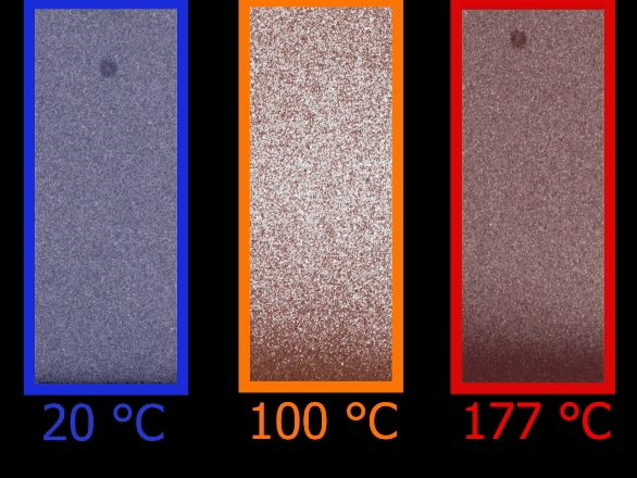
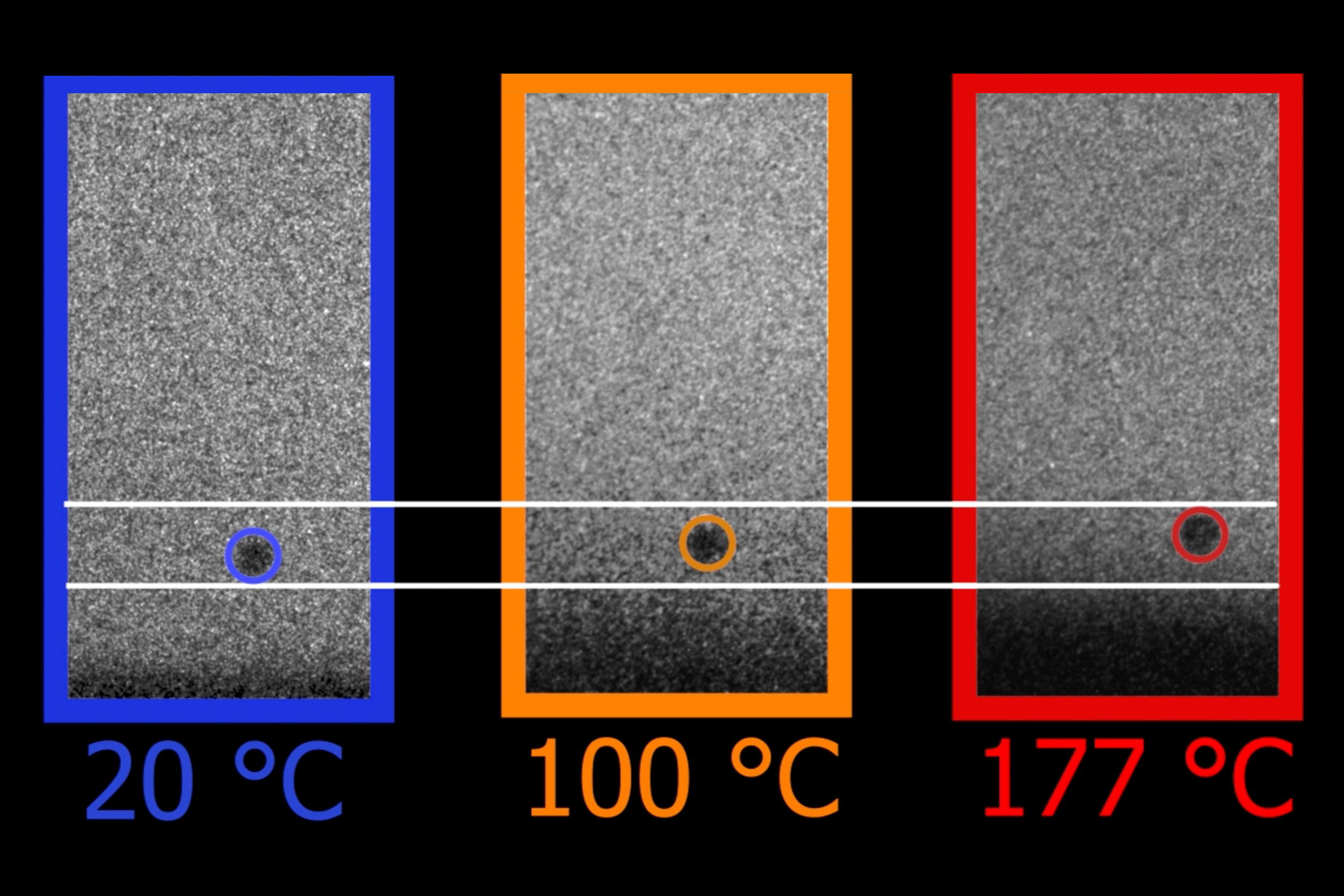
MIT scientists discovered that when metals are deformed at an extreme rate by an object moving at high velocities, hotter temperatures make the metal stronger, not weaker. Here, 3 particles are hitting a metallic surface at about the same velocity. As the initial temperature of the metal is increased, the rebound is faster, and the particle bounces higher because the metal becomes harder not softer, too.
Engineers at MIT, Nanyang Technological University, and several companies have developed a compact and inexpensive technology for detecting and measuring lead concentrations in water, potentially enabling a significant advance in tackling this persistent global health issue.
The World Health Organization estimates that 240 million people worldwide are exposed to drinking water that contains unsafe amounts of toxic lead, which can affect brain development in children, cause birth defects, and produce a variety of neurological, cardiac, and other damaging effects. In the United States alone, an estimated 10 million households still get drinking water delivered through lead pipes.
“It’s an unaddressed public health crisis that leads to over 1 million deaths annually,” says Jia Xu Brian Sia, an MIT postdoc and the senior author of the paper describing the new technology.
But testing for lead in water requires expensive, cumbersome equipment and typically requires days to get results. Or, it uses simple test strips that simply reveal a yes-or-no answer about the presence of lead but no information about its concentration. Current EPA regulations require drinking water to contain no more that 15 parts per billion of lead, a concentration so low it is difficult to detect.
The new system, which could be ready for commercial deployment within two or three years, could detect lead concentrations as low as 1 part per billion, with high accuracy, using a simple chip-based detector housed in a handheld device. The technology gives nearly instant quantitative measurements and requires just a droplet of water.
The findings are described in a paper appearing today in the journal Nature Communications, by Sia, MIT graduate student and lead author Luigi Ranno, Professor Juejun Hu, and 12 others at MIT and other institutions in academia and industry.
The team set out to find a simple detection method based on the use of photonic chips, which use light to perform measurements. The challenging part was finding a way to attach to the photonic chip surface certain ring-shaped molecules known as crown ethers, which can capture specific ions such as lead. After years of effort, they were able to achieve that attachment via a chemical process known as Fischer esterification. “That is one of the essential breakthroughs we have made in this technology,” Sia says.
In testing the new chip, the researchers showed that it can detect lead in water at concentrations as low as one part per billion. At much higher concentrations, which may be relevant for testing environmental contamination such as mine tailings, the accuracy is within 4 percent.
The device works in water with varying levels of acidity, ranging from pH values of 6 to 8, “which covers most environmental samples,” Sia says. They have tested the device with seawater as well as tap water, and verified the accuracy of the measurements.
In order to achieve such levels of accuracy, current testing requires a device called an inductive coupled plasma mass spectrometer. “These setups can be big and expensive,” Sia says. The sample processing can take days and requires experienced technical personnel.
While the new chip system they developed is “the core part of the innovation,” Ranno says, further work will be needed to develop this into an integrated, handheld device for practical use. “For making an actual product, you would need to package it into a usable form factor,” he explains. This would involve having a small chip-based laser coupled to the photonic chip. “It’s a matter of mechanical design, some optical design, some chemistry, and figuring out the supply chain,” he says. While that takes time, he says, the underlying concepts are straightforward.
The system can be adapted to detect other similar contaminants in water, including cadmium, copper, lithium, barium, cesium, and radium, Ranno says. The device could be used with simple cartridges that can be swapped out to detect different elements, each using slightly different crown ethers that can bind to a specific ion.
“There’s this problem that people don’t measure their water enough, especially in the developing countries,” Ranno says. “And that’s because they need to collect the water, prepare the sample, and bring it to these huge instruments that are extremely expensive.” Instead, “having this handheld device, something compact that even untrained personnel can just bring to the source for on-site monitoring, at low costs,” could make regular, ongoing widespread testing feasible.
Hu, who is the John F. Elliott Professor of Materials Science and Engineering, says, “I’m hoping this will be quickly implemented, so we can benefit human society. This is a good example of a technology coming from a lab innovation where it may actually make a very tangible impact on society, which is of course very fulfilling.”
“If this study can be extended to simultaneous detection of multiple metal elements, especially the presently concerning radioactive elements, its potential would be immense,” says Hou Wang, an associate professor of environmental science and engineering at Hunan University in China, who was not associated with this work.
Wang adds, “This research has engineered a sensor capable of instantaneously detecting lead concentration in water. This can be utilized in real-time to monitor the lead pollution concentration in wastewater discharged from industries such as battery manufacturing and lead smelting, facilitating the establishment of industrial wastewater monitoring systems. I think the innovative aspects and developmental potential of this research are quite commendable.”
Wang Qian, a principal research scientist at A*STAR’s Institute of Materials Research in Singapore, who also was not affiliated with this work, says, “The ability for the pervasive, portable, and quantitative detection of lead has proved to be challenging primarily due to cost concerns. This work demonstrates the potential to do so in a highly integrated form factor and is compatible with large-scale, low-cost manufacturing.”
The team included researchers at MIT, at Nanyang Technological University and Temasek Laboratories in Singapore, at the University of Southampton in the U.K., and at companies Fingate Technologies, in Singapore, and Vulcan Photonics, headquartered in Malaysia. The work used facilities at MIT.nano, the Harvard University Center for Nanoscale Systems, NTU’s Center for Micro- and Nano-Electronics, and the Nanyang Nanofabrication Center.
Artist’s impression of the chip surface, showing the on-chip light interferometer used to sense the presence of lead. The lead binding process to the crown ether is shown in the inset.
It’s the most fundamental of processes — the evaporation of water from the surfaces of oceans and lakes, the burning off of fog in the morning sun, and the drying of briny ponds that leaves solid salt behind. Evaporation is all around us, and humans have been observing it and making use of it for as long as we have existed.
And yet, it turns out, we’ve been missing a major part of the picture all along.
In a series of painstakingly precise experiments, a team of researchers at MIT has demonstrated that heat isn’t alone in causing water to evaporate. Light, striking the water’s surface where air and water meet, can break water molecules away and float them into the air, causing evaporation in the absence of any source of heat.
The astonishing new discovery could have a wide range of significant implications. It could help explain mysterious measurements over the years of how sunlight affects clouds, and therefore affect calculations of the effects of climate change on cloud cover and precipitation. It could also lead to new ways of designing industrial processes such as solar-powered desalination or drying of materials.
The findings, and the many different lines of evidence that demonstrate the reality of the phenomenon and the details of how it works, are described today in the journal PNAS, in a paper by Carl Richard Soderberg Professor of Power Engineering Gang Chen, postdocs Guangxin Lv and Yaodong Tu, and graduate student James Zhang.
The authors say their study suggests that the effect should happen widely in nature— everywhere from clouds to fogs to the surfaces of oceans, soils, and plants — and that it could also lead to new practical applications, including in energy and clean water production. “I think this has a lot of applications,” Chen says. “We’re exploring all these different directions. And of course, it also affects the basic science, like the effects of clouds on climate, because clouds are the most uncertain aspect of climate models.”
A newfound phenomenon
The new work builds on research reported last year, which described this new “photomolecular effect” but only under very specialized conditions: on the surface of specially prepared hydrogels soaked with water. In the new study, the researchers demonstrate that the hydrogel is not necessary for the process; it occurs at any water surface exposed to light, whether it’s a flat surface like a body of water or a curved surface like a droplet of cloud vapor.
Because the effect was so unexpected, the team worked to prove its existence with as many different lines of evidence as possible. In this study, they report 14 different kinds of tests and measurements they carried out to establish that water was indeed evaporating — that is, molecules of water were being knocked loose from the water’s surface and wafted into the air — due to the light alone, not by heat, which was long assumed to be the only mechanism involved.
One key indicator, which showed up consistently in four different kinds of experiments under different conditions, was that as the water began to evaporate from a test container under visible light, the air temperature measured above the water’s surface cooled down and then leveled off, showing that thermal energy was not the driving force behind the effect.
Other key indicators that showed up included the way the evaporation effect varied depending on the angle of the light, the exact color of the light, and its polarization. None of these varying characteristics should happen because at these wavelengths, water hardly absorbs light at all — and yet the researchers observed them.
The effect is strongest when light hits the water surface at an angle of 45 degrees. It is also strongest with a certain type of polarization, called transverse magnetic polarization. And it peaks in green light — which, oddly, is the color for which water is most transparent and thus interacts the least.
Chen and his co-researchers have proposed a physical mechanism that can explain the angle and polarization dependence of the effect, showing that the photons of light can impart a net force on water molecules at the water surface that is sufficient to knock them loose from the body of water. But they cannot yet account for the color dependence, which they say will require further study.
They have named this the photomolecular effect, by analogy with the photoelectric effect that was discovered by Heinrich Hertz in 1887 and finally explained by Albert Einstein in 1905. That effect was one of the first demonstrations that light also has particle characteristics, which had major implications in physics and led to a wide variety of applications, including LEDs. Just as the photoelectric effect liberates electrons from atoms in a material in response to being hit by a photon of light, the photomolecular effect shows that photons can liberate entire molecules from a liquid surface, the researchers say.
“The finding of evaporation caused by light instead of heat provides new disruptive knowledge of light-water interaction,” says Xiulin Ruan, professor of mechanical engineering at Purdue University, who was not involved in the study. “It could help us gain new understanding of how sunlight interacts with cloud, fog, oceans, and other natural water bodies to affect weather and climate. It has significant potential practical applications such as high-performance water desalination driven by solar energy. This research is among the rare group of truly revolutionary discoveries which are not widely accepted by the community right away but take time, sometimes a long time, to be confirmed.”
Solving a cloud conundrum
The finding may solve an 80-year-old mystery in climate science. Measurements of how clouds absorb sunlight have often shown that they are absorbing more sunlight than conventional physics dictates possible. The additional evaporation caused by this effect could account for the longstanding discrepancy, which has been a subject of dispute since such measurements are difficult to make.
“Those experiments are based on satellite data and flight data,“ Chen explains. “They fly an airplane on top of and below the clouds, and there are also data based on the ocean temperature and radiation balance. And they all conclude that there is more absorption by clouds than theory could calculate. However, due to the complexity of clouds and the difficulties of making such measurements, researchers have been debating whether such discrepancies are real or not. And what we discovered suggests that hey, there’s another mechanism for cloud absorption, which was not accounted for, and this mechanism might explain the discrepancies.”
Chen says he recently spoke about the phenomenon at an American Physical Society conference, and one physicist there who studies clouds and climate said they had never thought about this possibility, which could affect calculations of the complex effects of clouds on climate. The team conducted experiments using LEDs shining on an artificial cloud chamber, and they observed heating of the fog, which was not supposed to happen since water does not absorb in the visible spectrum. “Such heating can be explained based on the photomolecular effect more easily,” he says.
Lv says that of the many lines of evidence, “the flat region in the air-side temperature distribution above hot water will be the easiest for people to reproduce.” That temperature profile “is a signature” that demonstrates the effect clearly, he says.
Zhang adds: “It is quite hard to explain how this kind of flat temperature profile comes about without invoking some other mechanism” beyond the accepted theories of thermal evaporation. “It ties together what a whole lot of people are reporting in their solar desalination devices,” which again show evaporation rates that cannot be explained by the thermal input.
The effect can be substantial. Under the optimum conditions of color, angle, and polarization, Lv says, “the evaporation rate is four times the thermal limit.”
Already, since publication of the first paper, the team has been approached by companies that hope to harness the effect, Chen says, including for evaporating syrup and drying paper in a paper mill. The likeliest first applications will come in the areas of solar desalinization systems or other industrial drying processes, he says. “Drying consumes 20 percent of all industrial energy usage,” he points out.
Because the effect is so new and unexpected, Chen says, “This phenomenon should be very general, and our experiment is really just the beginning.” The experiments needed to demonstrate and quantify the effect are very time-consuming. “There are many variables, from understanding water itself, to extending to other materials, other liquids and even solids,” he says.
“The observations in the manuscript points to a new physical mechanism that foundationally alters our thinking on the kinetics of evaporation,” says Shannon Yee, an associate professor of mechanical engineering at Georgia Tech, who was not associated with this work. He adds, “Who would have thought that we are still learning about something as quotidian as water evaporating?”
“I think this work is very significant scientifically because it presents a new mechanism,” says University of Alberta Distinguished Professor Janet A.W. Elliott, who also was not associated with this work. “It may also turn out to be practically important for technology and our understanding of nature, because evaporation of water is ubiquitous and the effect appears to deliver significantly higher evaporation rates than the known thermal mechanism. … My overall impression is this work is outstanding. It appears to be carefully done with many precise experiments lending support for one another.”
The work was partly supported by an MIT Bose Award. The authors are currently working on ways to make use of this effect for water desalination, in a project funded by the Abdul Latif Jameel Water and Food Systems Lab and the MIT-UMRP program.
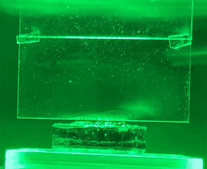
Researchers at MIT have discovered a new phenomenon: that light can cause evaporation of water from its surface without the need for heat. Pictured is a lab device designed to measure the “photomolecular effect,” using laser beams.
Neutrons are subatomic particles that have no electric charge, unlike protons and electrons. That means that while the electromagnetic force is responsible for most of the interactions between radiation and materials, neutrons are essentially immune to that force.
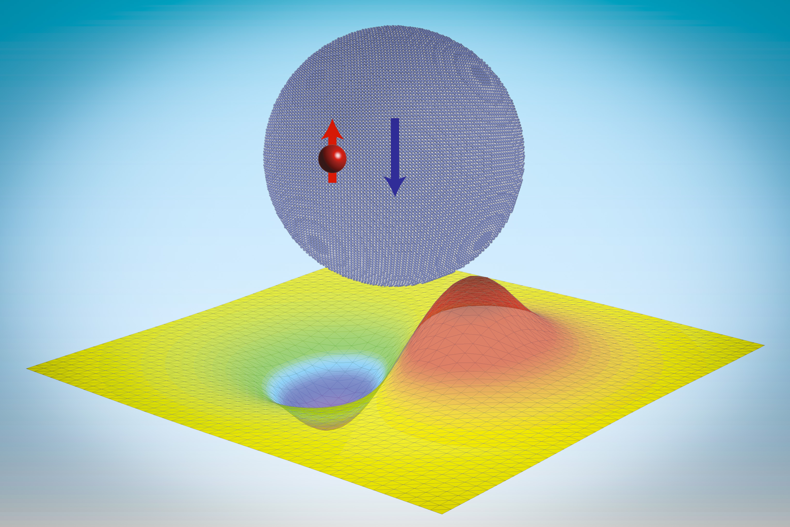
Instead, neutrons are held together inside an atom’s nucleus solely by something called the strong force, one of the four fundamental forces of nature. As its name implies, the force is indeed very strong, but only at very close range — it drops off so rapidly as to be negligible beyond 1/10,000 the size of an atom. But now, researchers at MIT have found that neutrons can actually be made to cling to particles called quantum dots, which are made up of tens of thousands of atomic nuclei, held there just by the strong force.
The new finding may lead to useful new tools for probing the basic properties of materials at the quantum level, including those arising from the strong force, as well as exploring new kinds of quantum information processing devices. The work is reported this week in the journal ACS Nano, in a paper by MIT graduate students Hao Tang and Guoqing Wang and MIT professors Ju Li and Paola Cappellaro of the Department of Nuclear Science and Engineering.
Neutrons are widely used to probe material properties using a method called neutron scattering, in which a beam of neutrons is focused on a sample, and the neutrons that bounce off the material’s atoms can be detected to reveal the material’s internal structure and dynamics.
But until this new work, nobody thought that these neutrons might actually stick to the materials they were probing. “The fact that [the neutrons] can be trapped by the materials, nobody seems to know about that,” says Li, who is also a professor of materials science and engineering. “We were surprised that this exists, and that nobody had talked about it before, among the experts we had checked with,” he says.
The reason this new finding is so surprising, Li explains, is because neutrons don’t interact with electromagnetic forces. Of the four fundamental forces, gravity and the weak force “are generally not important for materials,” he says. “Pretty much everything is electromagnetic interaction, but in this case, since the neutron doesn’t have a charge, the interaction here is through the strong interaction, and we know that is very short-range. It is effective at a range of 10 to the minus 15 power,” or one quadrillionth, of a meter.
“It’s very small, but it’s very intense,” he says of this force that holds the nuclei of atoms together. “But what’s interesting is we’ve got these many thousands of nuclei in this neutronic quantum dot, and that’s able to stabilize these bound states, which have much more diffuse wavefunctions at tens of nanometers [billionths of a meter]. These neutronic bound states in a quantum dot are actually quite akin to Thomson’s plum pudding model of an atom, after his discovery of the electron.”
It was so unexpected, Li calls it “a pretty crazy solution to a quantum mechanical problem.” The team calls the newly discovered state an artificial “neutronic molecule.”
These neutronic molecules are made from quantum dots, which are tiny crystalline particles, collections of atoms so small that their properties are governed more by the exact size and shape of the particles than by their composition. The discovery and controlled production of quantum dots were the subject of the 2023 Nobel Prize in Chemistry, awarded to MIT Professor Moungi Bawendi and two others.
“In conventional quantum dots, an electron is trapped by the electromagnetic potential created by a macroscopic number of atoms, thus its wavefunction extends to about 10 nanometers, much larger than a typical atomic radius,” says Cappellaro. “Similarly, in these nucleonic quantum dots, a single neutron can be trapped by a nanocrystal, with a size well beyond the range of the nuclear force, and display similar quantized energies.” While these energy jumps give quantum dots their colors, the neutronic quantum dots could be used for storing quantum information.
This work is based on theoretical calculations and computational simulations. “We did it analytically in two different ways, and eventually also verified it numerically,” Li says. Although the effect had never been described before, he says, in principle there’s no reason it couldn’t have been found much sooner: “Conceptually, people should have already thought about it,” he says, but as far as the team has been able to determine, nobody did.
Part of the difficulty in doing the computations is the very different scales involved: The binding energy of a neutron to the quantum dots they were attaching to is about one-trillionth that of previously known conditions where the neutron is bound to a small group of nucleons. For this work, the team used an analytical tool called Green’s function to demonstrate that the strong force was sufficient to capture neutrons with a quantum dot with a minimum radius of 13 nanometers.
Then, the researchers did detailed simulations of specific cases, such as the use of a lithium hydride nanocrystal, a material being studied as a possible storage medium for hydrogen. They showed that the binding energy of the neutrons to the nanocrystal is dependent on the exact dimensions and shape of the crystal, as well as the nuclear spin polarizations of the nuclei compared to that of the neutron. They also calculated similar effects for thin films and wires of the material as opposed to particles.
But Li says that actually creating such neutronic molecules in the lab, which among other things requires specialized equipment to maintain temperatures in the range of a few thousandths of a Kelvin above absolute zero, is something that other researchers with the appropriate expertise will have to undertake.
Li notes that “artificial atoms” made up of assemblages of atoms that share properties and can behave in many ways like a single atom have been used to probe many properties of real atoms. Similarly, he says, these artificial molecules provide “an interesting model system” that might be used to study “interesting quantum mechanical problems that one can think about,” such as whether these neutronic molecules will have a shell structure that mimics the electron shell structure of atoms.
“One possible application,” he says, “is maybe we can precisely control the neutron state. By changing the way the quantum dot oscillates, maybe we can shoot the neutron off in a particular direction.” Neutrons are powerful tools for such things as triggering both fission and fusion reactions, but so far it has been difficult to control individual neutrons. These new bound states could provide much greater degrees of control over individual neutrons, which could play a role in the development of new quantum information systems, he says.
“One idea is to use it to manipulate the neutron, and then the neutron will be able to affect other nuclear spins,” Li says. In that sense, he says, the neutronic molecule could serve as a mediator between the nuclear spins of separate nuclei — and this nuclear spin is a property that is already being used as a basic storage unit, or qubit, in developing quantum computer systems.
“The nuclear spin is like a stationary qubit, and the neutron is like a flying qubit,” he says. “That’s one potential application.” He adds that this is “quite different from electromagnetics-based quantum information processing, which is so far the dominant paradigm. So, regardless of whether it’s superconducting qubits or it’s trapped ions or nitrogen vacancy centers, most of these are based on electromagnetic interactions.” In this new system, instead, “we have neutrons and nuclear spin. We’re just starting to explore what we can do with it now.”
Another possible application, he says, is for a kind of imaging, using neutral activation analysis. “Neutron imaging complements X-ray imaging because neutrons are much more strongly interacting with light elements,” Li says. It can also be used for materials analysis, which can provide information not only about elemental composition but even about the different isotopes of those elements. “A lot of the chemical imaging and spectroscopy doesn’t tell us about the isotopes,” whereas the neutron-based method could do so, he says.
The research was supported by the U.S. Office of Naval Research.
MIT researchers discovered “neutronic” molecules, in which neutrons can be made to cling to quantum dots, held just by the strong force. The finding may lead to new tools for probing material properties at the quantum level and exploring new kinds of quantum information processing devices. Here, the red item represents a bound neutron, the sphere is a hydride nanoparticle, and the yellow field represents a neutron wavefunction.
Perovskites, a broad class of compounds with a particular kind of crystal structure, have long been seen as a promising alternative or supplement to today’s silicon or cadmium telluride solar panels. They could be far more lightweight and inexpensive, and could be coated onto virtually any substrate, including paper or flexible plastic that could be rolled up for easy transport.
In their efficiency at converting sunlight to electricity, perovskites are becoming comparable to silicon, whose manufacture still requires long, complex, and energy-intensive processes. One big remaining drawback is longevity: They tend to break down in a matter of months to years, while silicon solar panels can last more than two decades. And their efficiency over large module areas still lags behind silicon. Now, a team of researchers at MIT and several other institutions has revealed ways to optimize efficiency and better control degradation, by engineering the nanoscale structure of perovskite devices.
The study reveals new insights on how to make high-efficiency perovskite solar cells, and also provides new directions for engineers working to bring these solar cells to the commercial marketplace. The work is described today in the journal Nature Energy, in a paper by Dane deQuilettes, a recent MIT postdoc who is now co-founder and chief science officer of the MIT spinout Optigon, along with MIT professors Vladimir Bulovic and Moungi Bawendi, and 10 others at MIT and in Washington state, the U.K., and Korea.
“Ten years ago, if you had asked us what would be the ultimate solution to the rapid development of solar technologies, the answer would have been something that works as well as silicon but whose manufacturing is much simpler,” Bulovic says. “And before we knew it, the field of perovskite photovoltaics appeared. They were as efficient as silicon, and they were as easy to paint on as it is to paint on a piece of paper. The result was tremendous excitement in the field.”
Nonetheless, “there are some significant technical challenges of handling and managing this material in ways we’ve never done before,” he says. But the promise is so great that many hundreds of researchers around the world have been working on this technology. The new study looks at a very small but key detail: how to “passivate” the material’s surface, changing its properties in such a way that the perovskite no longer degrades so rapidly or loses efficiency.
“The key is identifying the chemistry of the interfaces, the place where the perovskite meets other materials,” Bulovic says, referring to the places where different materials are stacked next to perovskite in order to facilitate the flow of current through the device.
Engineers have developed methods for passivation, for example by using a solution that creates a thin passivating coating. But they’ve lacked a detailed understanding of how this process works — which is essential to make further progress in finding better coatings. The new study “addressed the ability to passivate those interfaces and elucidate the physics and science behind why this passivation works as well as it does,” Bulovic says.
The team used some of the most powerful instruments available at laboratories around the world to observe the interfaces between the perovskite layer and other materials, and how they develop, in unprecedented detail. This close examination of the passivation coating process and its effects resulted in “the clearest roadmap as of yet of what we can do to fine-tune the energy alignment at the interfaces of perovskites and neighboring materials,” and thus improve their overall performance, Bulovic says.
While the bulk of a perovskite material is in the form of a perfectly ordered crystalline lattice of atoms, this order breaks down at the surface. There may be extra atoms sticking out or vacancies where atoms are missing, and these defects cause losses in the material’s efficiency. That’s where the need for passivation comes in.
“This paper is essentially revealing a guidebook for how to tune surfaces, where a lot of these defects are, to make sure that energy is not lost at surfaces,” deQuilettes says. “It’s a really big discovery for the field,” he says. “This is the first paper that demonstrates how to systematically control and engineer surface fields in perovskites.”
The common passivation method is to bathe the surface in a solution of a salt called hexylammonium bromide, a technique developed at MIT several years ago by Jason Jungwan Yoo PhD ’20, who is a co-author of this paper, that led to multiple new world-record efficiencies. By doing that “you form a very thin layer on top of your defective surface, and that thin layer actually passivates a lot of the defects really well,” deQuilettes says. “And then the bromine, which is part of the salt, actually penetrates into the three-dimensional layer in a controllable way.” That penetration helps to prevent electrons from losing energy to defects at the surface.
These two effects, produced by a single processing step, produces the two beneficial changes simultaneously. “It’s really beautiful because usually you need to do that in two steps,” deQuilettes says.
The passivation reduces the energy loss of electrons at the surface after they have been knocked loose by sunlight. These losses reduce the overall efficiency of the conversion of sunlight to electricity, so reducing the losses boosts the net efficiency of the cells.
That could rapidly lead to improvements in the materials’ efficiency in converting sunlight to electricity, he says. The recent efficiency records for a single perovskite layer, several of them set at MIT, have ranged from about 24 to 26 percent, while the maximum theoretical efficiency that could be reached is about 30 percent, according to deQuilettes.
An increase of a few percent may not sound like much, but in the solar photovoltaic industry such improvements are highly sought after. “In the silicon photovoltaic industry, if you’re gaining half of a percent in efficiency, that’s worth hundreds of millions of dollars on the global market,” he says. A recent shift in silicon cell design, essentially adding a thin passivating layer and changing the doping profile, provides an efficiency gain of about half of a percent. As a result, “the whole industry is shifting and rapidly trying to push to get there.” The overall efficiency of silicon solar cells has only seen very small incremental improvements for the last 30 years, he says.
The record efficiencies for perovskites have mostly been set in controlled laboratory settings with small postage-stamp-size samples of the material. “Translating a record efficiency to commercial scale takes a long time,” deQuilettes says. “Another big hope is that with this understanding, people will be able to better engineer large areas to have these passivating effects.”
There are hundreds of different kinds of passivating salts and many different kinds of perovskites, so the basic understanding of the passivation process provided by this new work could help guide researchers to find even better combinations of materials, the researchers suggest. “There are so many different ways you could engineer the materials,” he says.
“I think we are on the doorstep of the first practical demonstrations of perovskites in the commercial applications,” Bulovic says. “And those first applications will be a far cry from what we’ll be able to do a few years from now.” He adds that perovskites “should not be seen as a displacement of silicon photovoltaics. It should be seen as an augmentation — yet another way to bring about more rapid deployment of solar electricity.”
“A lot of progress has been made in the last two years on finding surface treatments that improve perovskite solar cells,” says Michael McGehee, a professor of chemical engineering at the University of Colorado who was not associated with this research. “A lot of the research has been empirical with the mechanisms behind the improvements not being fully understood. This detailed study shows that treatments can not only passivate defects, but can also create a surface field that repels carriers that should be collected at the other side of the device. This understanding might help further improve the interfaces.”
The team included researchers at the Korea Research Institute of Chemical Technology, Cambridge University, the University of Washington in Seattle, and Sungkyunkwan University in Korea. The work was supported by the Tata Trust, the MIT Institute for Soldier Nanotechnologies, the U.S. Department of Energy, and the U.S. National Science Foundation.
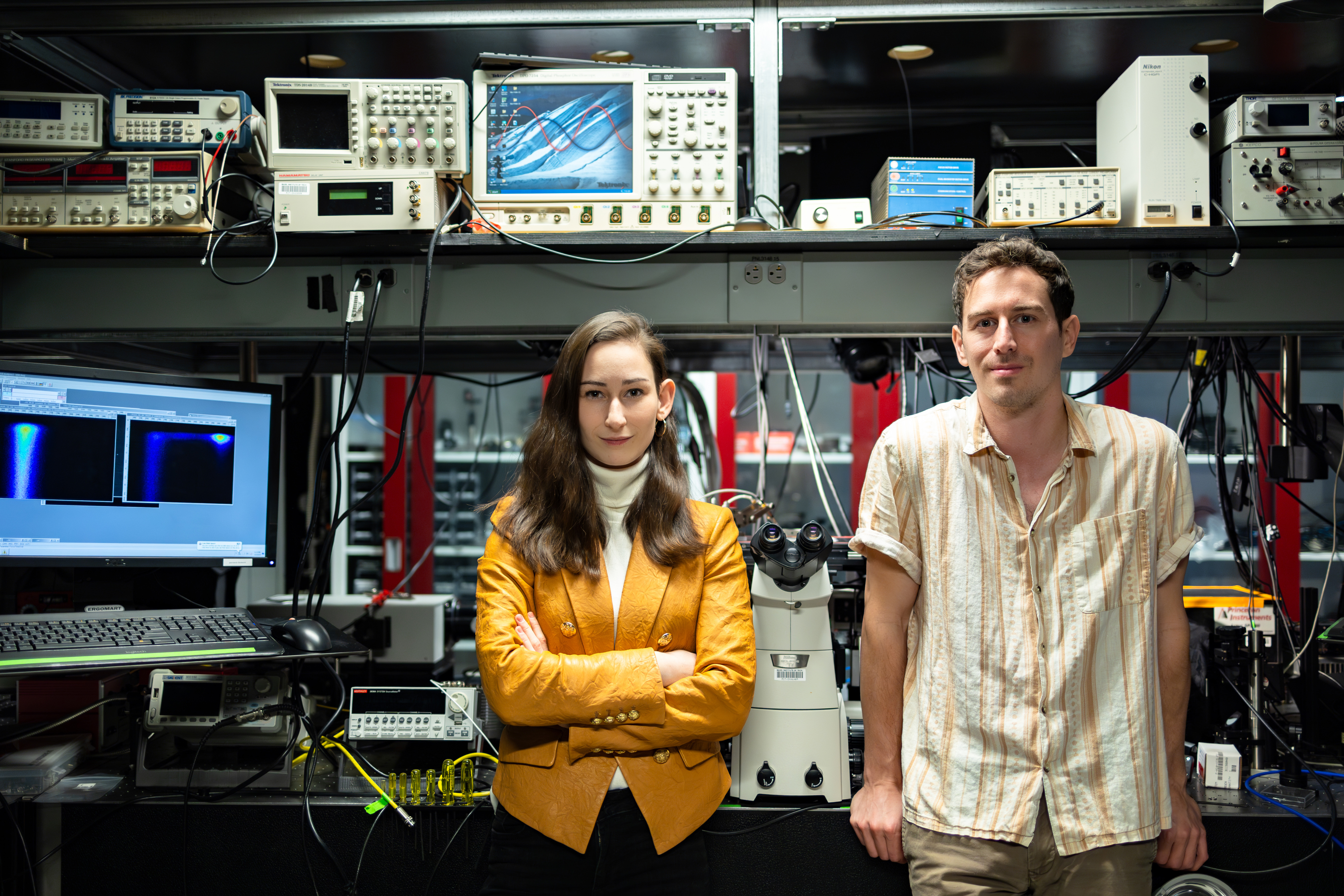
A team of MIT researchers and several other institutions has revealed ways to optimize efficiency and better control degradation, by engineering the nanoscale structure of perovskite devices. Team members include Madeleine Laitz, left, and lead author Dane deQuilettes.
Titanium alloys are essential structural materials for a wide variety of applications, from aerospace and energy infrastructure to biomedical equipment. But like most metals, optimizing their properties tends to involve a tradeoff between two key characteristics: strength and ductility. Stronger materials tend to be less deformable, and deformable materials tend to be mechanically weak.
Now, researchers at MIT, collaborating with researchers at ATI Specialty Materials, have discovered an approach for creating new titanium alloys that can exceed this historical tradeoff, leading to new alloys with exceptional combinations of strength and ductility, which might lead to new applications.
The findings are described in the journal Advanced Materials, in a paper by Shaolou Wei ScD ’22, Professor C. Cem Tasan, postdoc Kyung-Shik Kim, and John Foltz from ATI Inc. The improvements, the team says, arise from tailoring the chemical composition and the lattice structure of the alloy, while also adjusting the processing techniques used to produce the material at industrial scale.
Titanium alloys have been important because of their exceptional mechanical properties, corrosion resistance, and light weight when compared to steels for example. Through careful selection of the alloying elements and their relative proportions, and of the way the material is processed, “you can create various different structures, and this creates a big playground for you to get good property combinations, both for cryogenic and elevated temperatures,” Tasan says.
But that big assortment of possibilities in turn requires a way to guide the selections to produce a material that meets the specific needs of a particular application. The analysis and experimental results described in the new study provide that guidance.
The structure of titanium alloys, all the way down to atomic scale, governs their properties, Tasan explains. And in some titanium alloys, this structure is even more complex, made up of two different intermixed phases, known as the alpha and beta phases.
“The key strategy in this design approach is to take considerations of different scales,” he says. “One scale is the structure of individual crystal. For example, by choosing the alloying elements carefully, you can have a more ideal crystal structure of the alpha phase that enables particular deformation mechanisms. The other scale is the polycrystal scale, that involves interactions of the alpha and beta phases. So, the approach that’s followed here involves design considerations for both.”
In addition to choosing the right alloying materials and proportions, steps in the processing turned out to play an important role. A technique called cross-rolling is another key to achieving the exceptional combination of strength and ductility, the team found.
Working together with ATI researchers, the team tested a variety of alloys under a scanning electron microscope as they were being deformed, revealing details of how their microstructures respond to external mechanical load. They found that there was a particular set of parameters — of composition, proportions, and processing method — that yielded a structure where the alpha and beta phases shared the deformation uniformly, mitigating the cracking tendency that is likely to occur between the phases when they respond differently. “The phases deform in harmony,” Tasan says. This cooperative response to deformation can yield a superior material, they found.
“We looked at the structure of the material to understand these two phases and their morphologies, and we looked at their chemistries by carrying out local chemical analysis at the atomic scale. We adopted a wide variety of techniques to quantify various properties of the material across multiple length scales, says Tasan, who is the POSCO Professor of Materials Science and Engineering and an associate professor of metallurgy. “When we look at the overall properties” of the titanium alloys produced according to their system, “the properties are really much better than comparable alloys.”
This was industry-supported academic research aimed at proving design principles for alloys that can be commercially produced at scale, according to Tasan. “What we do in this collaboration is really toward a fundamental understanding of crystal plasticity,” he says. “We show that this design strategy is validated, and we show scientifically how it works,” he adds, noting that there remains significant room for further improvement.
As for potential applications of these findings, he says, “for any aerospace application where an improved combination of strength and ductility are useful, this kind of invention is providing new opportunities.”
The work was supported by ATI Specialty Rolled Products and used facilities of MIT.nano and the Center for Nanoscale Systems at Harvard University.
Metals get softer when they are heated, which is how blacksmiths can form iron into complex shapes by heating it red hot. And anyone who compares a copper wire with a steel coat hanger will quickly discern that copper is much more pliable than steel.
But scientists at MIT have discovered that when metal is struck by an object moving at a super high velocity, the opposite happens: The hotter the metal, the stronger it is. Under those conditions, which put extreme stress on the metal, copper can actually be just as strong as steel. The new discovery could lead to new approaches to designing materials for extreme environments, such as shields that protect spacecraft or hypersonic aircraft, or equipment for high-speed manufacturing processes.
The findings are described in a paper appearing today in the journal Nature, by Ian Dowding, an MIT graduate student, and Christopher Schuh, former head of MIT’s Department of Materials Science and Engineering, now dean of engineering at Northwestern University and visiting professor at MIT.
The new finding, the authors write, “is counterintuitive and at odds with decades of studies in less extreme conditions.” The unexpected results could affect a variety of applications because the extreme velocities involved in these impacts occur routinely in meteorite impacts on spacecraft in orbit and in high-speed machining operations used in manufacturing, sandblasting, and some additive manufacturing (3D printing) processes.
The experiments the researchers used to find this effect involved shooting tiny particles of sapphire, just millionths of a meter across, at flat sheets of metal. Propelled by laser beams, the particles reached high velocities, on the order of a few hundred meters per second. While other researchers have occasionally done experiments at similarly high velocities, they have tended to use larger impactors, at the scale of centimeters or larger. Because these larger impacts were dominated by effects of the shock of the impact, there was no way to separate out the mechanical and thermal effects.
The tiny particles in the new study don’t create a significant pressure wave when they hit the target. But it has taken a decade of research at MIT to develop methods of propelling such microscopic particles at such high velocities. “We’ve taken advantage of that,” Schuh says, along with other new techniques for observing the high-speed impact itself.
The team used extremely high-speed cameras “to watch the particles as they come in and as they fly away,” he says. As the particles bounce off the surface, the difference between the incoming and outgoing velocities “tells you how much energy was deposited” into the target, which is an indicator of the surface strength.
The tiny particles they used were made of alumina, or sapphire, and are “very hard,” Dowding says. At 10 to 20 microns (millionths of a meter) across, these are between one-tenth and one-fifth of the thickness of a human hair. When the launchpad behind those particles is hit by a laser beam, part of the material vaporizes, creating a jet of vapor that propels the particle in the opposite direction.
The researchers shot the particles at samples of copper, titanium, and gold, and they expect their results should apply to other metals as well. They say their data provide the first direct experimental evidence for this anomalous thermal effect of increased strength with greater heat, although hints of such an effect had been reported before.
The surprising effect appears to result from the way the orderly arrays of atoms that make up the crystalline structure of metals move under different conditions, according to the researchers’ analysis. They show that there are three separate effects governing how metal deforms under stress, and while two of these follow the predicted trajectory of increasing deformation at higher temperatures, it is the third effect, called drag strengthening, that reverses its effect when the deformation rate crosses a certain threshold.
Beyond this crossover point, the higher temperature increases the activity of phonons — waves of sound or heat — within the material, and these phonons interact with dislocations in the crystalline lattice in a way that limits their ability to slip and deform. The effect increases with increased impact speed and temperature, Dowding says, so that “the faster you go, the less the dislocations are able to respond.”
Of course, at some point the increased temperature will begin to melt the metal, and at that point the effect will reverse again and lead to softening. “There will be a limit” to this strengthening effect, Dowding says, “but we don’t know what it is.”
The findings could lead to different choices of materials when designing devices that may encounter such extreme stresses, Schuh says. For example, metals that may ordinarily be much weaker, but that are less expensive or easier to process, might be useful in situations where nobody would have thought to use them before.
The extreme conditions the researchers studied are not confined to spacecraft or extreme manufacturing methods. “If you are flying a helicopter in a sandstorm, a lot of these sand particles will reach high velocities as they hit the blades,” Dowding says, and under desert conditions they may reach the high temperatures where these hardening effects kick in.
The techniques the researchers used to uncover this phenomenon could be applied to a variety of other materials and situations, including other metals and alloys. Designing materials to be used in extreme conditions by simply extrapolating from known properties at less extreme conditions could lead to seriously mistaken expectations about how materials will behave under extreme stresses, they say.
The research was supported by the U.S. Department of Energy.
MIT scientists discovered that when metals are deformed at an extreme rate by an object moving at high velocities, hotter temperatures make the metal stronger, not weaker. Here, 3 particles are hitting a metallic surface at about the same velocity. As the initial temperature of the metal is increased, the rebound is faster, and the particle bounces higher because the metal becomes harder not softer, too.
Engineers at MIT, Nanyang Technological University, and several companies have developed a compact and inexpensive technology for detecting and measuring lead concentrations in water, potentially enabling a significant advance in tackling this persistent global health issue.
The World Health Organization estimates that 240 million people worldwide are exposed to drinking water that contains unsafe amounts of toxic lead, which can affect brain development in children, cause birth defects, and produce a variety of neurological, cardiac, and other damaging effects. In the United States alone, an estimated 10 million households still get drinking water delivered through lead pipes.
“It’s an unaddressed public health crisis that leads to over 1 million deaths annually,” says Jia Xu Brian Sia, an MIT postdoc and the senior author of the paper describing the new technology.
But testing for lead in water requires expensive, cumbersome equipment and typically requires days to get results. Or, it uses simple test strips that simply reveal a yes-or-no answer about the presence of lead but no information about its concentration. Current EPA regulations require drinking water to contain no more that 15 parts per billion of lead, a concentration so low it is difficult to detect.
The new system, which could be ready for commercial deployment within two or three years, could detect lead concentrations as low as 1 part per billion, with high accuracy, using a simple chip-based detector housed in a handheld device. The technology gives nearly instant quantitative measurements and requires just a droplet of water.
The findings are described in a paper appearing today in the journal Nature Communications, by Sia, MIT graduate student and lead author Luigi Ranno, Professor Juejun Hu, and 12 others at MIT and other institutions in academia and industry.
The team set out to find a simple detection method based on the use of photonic chips, which use light to perform measurements. The challenging part was finding a way to attach to the photonic chip surface certain ring-shaped molecules known as crown ethers, which can capture specific ions such as lead. After years of effort, they were able to achieve that attachment via a chemical process known as Fischer esterification. “That is one of the essential breakthroughs we have made in this technology,” Sia says.
In testing the new chip, the researchers showed that it can detect lead in water at concentrations as low as one part per billion. At much higher concentrations, which may be relevant for testing environmental contamination such as mine tailings, the accuracy is within 4 percent.
The device works in water with varying levels of acidity, ranging from pH values of 6 to 8, “which covers most environmental samples,” Sia says. They have tested the device with seawater as well as tap water, and verified the accuracy of the measurements.
In order to achieve such levels of accuracy, current testing requires a device called an inductive coupled plasma mass spectrometer. “These setups can be big and expensive,” Sia says. The sample processing can take days and requires experienced technical personnel.
While the new chip system they developed is “the core part of the innovation,” Ranno says, further work will be needed to develop this into an integrated, handheld device for practical use. “For making an actual product, you would need to package it into a usable form factor,” he explains. This would involve having a small chip-based laser coupled to the photonic chip. “It’s a matter of mechanical design, some optical design, some chemistry, and figuring out the supply chain,” he says. While that takes time, he says, the underlying concepts are straightforward.
The system can be adapted to detect other similar contaminants in water, including cadmium, copper, lithium, barium, cesium, and radium, Ranno says. The device could be used with simple cartridges that can be swapped out to detect different elements, each using slightly different crown ethers that can bind to a specific ion.
“There’s this problem that people don’t measure their water enough, especially in the developing countries,” Ranno says. “And that’s because they need to collect the water, prepare the sample, and bring it to these huge instruments that are extremely expensive.” Instead, “having this handheld device, something compact that even untrained personnel can just bring to the source for on-site monitoring, at low costs,” could make regular, ongoing widespread testing feasible.
Hu, who is the John F. Elliott Professor of Materials Science and Engineering, says, “I’m hoping this will be quickly implemented, so we can benefit human society. This is a good example of a technology coming from a lab innovation where it may actually make a very tangible impact on society, which is of course very fulfilling.”
“If this study can be extended to simultaneous detection of multiple metal elements, especially the presently concerning radioactive elements, its potential would be immense,” says Hou Wang, an associate professor of environmental science and engineering at Hunan University in China, who was not associated with this work.
Wang adds, “This research has engineered a sensor capable of instantaneously detecting lead concentration in water. This can be utilized in real-time to monitor the lead pollution concentration in wastewater discharged from industries such as battery manufacturing and lead smelting, facilitating the establishment of industrial wastewater monitoring systems. I think the innovative aspects and developmental potential of this research are quite commendable.”
Wang Qian, a principal research scientist at A*STAR’s Institute of Materials Research in Singapore, who also was not affiliated with this work, says, “The ability for the pervasive, portable, and quantitative detection of lead has proved to be challenging primarily due to cost concerns. This work demonstrates the potential to do so in a highly integrated form factor and is compatible with large-scale, low-cost manufacturing.”
The team included researchers at MIT, at Nanyang Technological University and Temasek Laboratories in Singapore, at the University of Southampton in the U.K., and at companies Fingate Technologies, in Singapore, and Vulcan Photonics, headquartered in Malaysia. The work used facilities at MIT.nano, the Harvard University Center for Nanoscale Systems, NTU’s Center for Micro- and Nano-Electronics, and the Nanyang Nanofabrication Center.
Artist’s impression of the chip surface, showing the on-chip light interferometer used to sense the presence of lead. The lead binding process to the crown ether is shown in the inset.
It’s the most fundamental of processes — the evaporation of water from the surfaces of oceans and lakes, the burning off of fog in the morning sun, and the drying of briny ponds that leaves solid salt behind. Evaporation is all around us, and humans have been observing it and making use of it for as long as we have existed.
And yet, it turns out, we’ve been missing a major part of the picture all along.
In a series of painstakingly precise experiments, a team of researchers at MIT has demonstrated that heat isn’t alone in causing water to evaporate. Light, striking the water’s surface where air and water meet, can break water molecules away and float them into the air, causing evaporation in the absence of any source of heat.
The astonishing new discovery could have a wide range of significant implications. It could help explain mysterious measurements over the years of how sunlight affects clouds, and therefore affect calculations of the effects of climate change on cloud cover and precipitation. It could also lead to new ways of designing industrial processes such as solar-powered desalination or drying of materials.
The findings, and the many different lines of evidence that demonstrate the reality of the phenomenon and the details of how it works, are described today in the journal PNAS, in a paper by Carl Richard Soderberg Professor of Power Engineering Gang Chen, postdocs Guangxin Lv and Yaodong Tu, and graduate student James Zhang.
The authors say their study suggests that the effect should happen widely in nature— everywhere from clouds to fogs to the surfaces of oceans, soils, and plants — and that it could also lead to new practical applications, including in energy and clean water production. “I think this has a lot of applications,” Chen says. “We’re exploring all these different directions. And of course, it also affects the basic science, like the effects of clouds on climate, because clouds are the most uncertain aspect of climate models.”
A newfound phenomenon
The new work builds on research reported last year, which described this new “photomolecular effect” but only under very specialized conditions: on the surface of specially prepared hydrogels soaked with water. In the new study, the researchers demonstrate that the hydrogel is not necessary for the process; it occurs at any water surface exposed to light, whether it’s a flat surface like a body of water or a curved surface like a droplet of cloud vapor.
Because the effect was so unexpected, the team worked to prove its existence with as many different lines of evidence as possible. In this study, they report 14 different kinds of tests and measurements they carried out to establish that water was indeed evaporating — that is, molecules of water were being knocked loose from the water’s surface and wafted into the air — due to the light alone, not by heat, which was long assumed to be the only mechanism involved.
One key indicator, which showed up consistently in four different kinds of experiments under different conditions, was that as the water began to evaporate from a test container under visible light, the air temperature measured above the water’s surface cooled down and then leveled off, showing that thermal energy was not the driving force behind the effect.
Other key indicators that showed up included the way the evaporation effect varied depending on the angle of the light, the exact color of the light, and its polarization. None of these varying characteristics should happen because at these wavelengths, water hardly absorbs light at all — and yet the researchers observed them.
The effect is strongest when light hits the water surface at an angle of 45 degrees. It is also strongest with a certain type of polarization, called transverse magnetic polarization. And it peaks in green light — which, oddly, is the color for which water is most transparent and thus interacts the least.
Chen and his co-researchers have proposed a physical mechanism that can explain the angle and polarization dependence of the effect, showing that the photons of light can impart a net force on water molecules at the water surface that is sufficient to knock them loose from the body of water. But they cannot yet account for the color dependence, which they say will require further study.
They have named this the photomolecular effect, by analogy with the photoelectric effect that was discovered by Heinrich Hertz in 1887 and finally explained by Albert Einstein in 1905. That effect was one of the first demonstrations that light also has particle characteristics, which had major implications in physics and led to a wide variety of applications, including LEDs. Just as the photoelectric effect liberates electrons from atoms in a material in response to being hit by a photon of light, the photomolecular effect shows that photons can liberate entire molecules from a liquid surface, the researchers say.
“The finding of evaporation caused by light instead of heat provides new disruptive knowledge of light-water interaction,” says Xiulin Ruan, professor of mechanical engineering at Purdue University, who was not involved in the study. “It could help us gain new understanding of how sunlight interacts with cloud, fog, oceans, and other natural water bodies to affect weather and climate. It has significant potential practical applications such as high-performance water desalination driven by solar energy. This research is among the rare group of truly revolutionary discoveries which are not widely accepted by the community right away but take time, sometimes a long time, to be confirmed.”
Solving a cloud conundrum
The finding may solve an 80-year-old mystery in climate science. Measurements of how clouds absorb sunlight have often shown that they are absorbing more sunlight than conventional physics dictates possible. The additional evaporation caused by this effect could account for the longstanding discrepancy, which has been a subject of dispute since such measurements are difficult to make.
“Those experiments are based on satellite data and flight data,“ Chen explains. “They fly an airplane on top of and below the clouds, and there are also data based on the ocean temperature and radiation balance. And they all conclude that there is more absorption by clouds than theory could calculate. However, due to the complexity of clouds and the difficulties of making such measurements, researchers have been debating whether such discrepancies are real or not. And what we discovered suggests that hey, there’s another mechanism for cloud absorption, which was not accounted for, and this mechanism might explain the discrepancies.”
Chen says he recently spoke about the phenomenon at an American Physical Society conference, and one physicist there who studies clouds and climate said they had never thought about this possibility, which could affect calculations of the complex effects of clouds on climate. The team conducted experiments using LEDs shining on an artificial cloud chamber, and they observed heating of the fog, which was not supposed to happen since water does not absorb in the visible spectrum. “Such heating can be explained based on the photomolecular effect more easily,” he says.
Lv says that of the many lines of evidence, “the flat region in the air-side temperature distribution above hot water will be the easiest for people to reproduce.” That temperature profile “is a signature” that demonstrates the effect clearly, he says.
Zhang adds: “It is quite hard to explain how this kind of flat temperature profile comes about without invoking some other mechanism” beyond the accepted theories of thermal evaporation. “It ties together what a whole lot of people are reporting in their solar desalination devices,” which again show evaporation rates that cannot be explained by the thermal input.
The effect can be substantial. Under the optimum conditions of color, angle, and polarization, Lv says, “the evaporation rate is four times the thermal limit.”
Already, since publication of the first paper, the team has been approached by companies that hope to harness the effect, Chen says, including for evaporating syrup and drying paper in a paper mill. The likeliest first applications will come in the areas of solar desalinization systems or other industrial drying processes, he says. “Drying consumes 20 percent of all industrial energy usage,” he points out.
Because the effect is so new and unexpected, Chen says, “This phenomenon should be very general, and our experiment is really just the beginning.” The experiments needed to demonstrate and quantify the effect are very time-consuming. “There are many variables, from understanding water itself, to extending to other materials, other liquids and even solids,” he says.
“The observations in the manuscript points to a new physical mechanism that foundationally alters our thinking on the kinetics of evaporation,” says Shannon Yee, an associate professor of mechanical engineering at Georgia Tech, who was not associated with this work. He adds, “Who would have thought that we are still learning about something as quotidian as water evaporating?”
“I think this work is very significant scientifically because it presents a new mechanism,” says University of Alberta Distinguished Professor Janet A.W. Elliott, who also was not associated with this work. “It may also turn out to be practically important for technology and our understanding of nature, because evaporation of water is ubiquitous and the effect appears to deliver significantly higher evaporation rates than the known thermal mechanism. … My overall impression is this work is outstanding. It appears to be carefully done with many precise experiments lending support for one another.”
The work was partly supported by an MIT Bose Award. The authors are currently working on ways to make use of this effect for water desalination, in a project funded by the Abdul Latif Jameel Water and Food Systems Lab and the MIT-UMRP program.
Researchers at MIT have discovered a new phenomenon: that light can cause evaporation of water from its surface without the need for heat. Pictured is a lab device designed to measure the “photomolecular effect,” using laser beams.
Neutrons are subatomic particles that have no electric charge, unlike protons and electrons. That means that while the electromagnetic force is responsible for most of the interactions between radiation and materials, neutrons are essentially immune to that force.
Instead, neutrons are held together inside an atom’s nucleus solely by something called the strong force, one of the four fundamental forces of nature. As its name implies, the force is indeed very strong, but only at very close range — it drops off so rapidly as to be negligible beyond 1/10,000 the size of an atom. But now, researchers at MIT have found that neutrons can actually be made to cling to particles called quantum dots, which are made up of tens of thousands of atomic nuclei, held there just by the strong force.
The new finding may lead to useful new tools for probing the basic properties of materials at the quantum level, including those arising from the strong force, as well as exploring new kinds of quantum information processing devices. The work is reported this week in the journal ACS Nano, in a paper by MIT graduate students Hao Tang and Guoqing Wang and MIT professors Ju Li and Paola Cappellaro of the Department of Nuclear Science and Engineering.
Neutrons are widely used to probe material properties using a method called neutron scattering, in which a beam of neutrons is focused on a sample, and the neutrons that bounce off the material’s atoms can be detected to reveal the material’s internal structure and dynamics.
But until this new work, nobody thought that these neutrons might actually stick to the materials they were probing. “The fact that [the neutrons] can be trapped by the materials, nobody seems to know about that,” says Li, who is also a professor of materials science and engineering. “We were surprised that this exists, and that nobody had talked about it before, among the experts we had checked with,” he says.
The reason this new finding is so surprising, Li explains, is because neutrons don’t interact with electromagnetic forces. Of the four fundamental forces, gravity and the weak force “are generally not important for materials,” he says. “Pretty much everything is electromagnetic interaction, but in this case, since the neutron doesn’t have a charge, the interaction here is through the strong interaction, and we know that is very short-range. It is effective at a range of 10 to the minus 15 power,” or one quadrillionth, of a meter.
“It’s very small, but it’s very intense,” he says of this force that holds the nuclei of atoms together. “But what’s interesting is we’ve got these many thousands of nuclei in this neutronic quantum dot, and that’s able to stabilize these bound states, which have much more diffuse wavefunctions at tens of nanometers [billionths of a meter]. These neutronic bound states in a quantum dot are actually quite akin to Thomson’s plum pudding model of an atom, after his discovery of the electron.”
It was so unexpected, Li calls it “a pretty crazy solution to a quantum mechanical problem.” The team calls the newly discovered state an artificial “neutronic molecule.”
These neutronic molecules are made from quantum dots, which are tiny crystalline particles, collections of atoms so small that their properties are governed more by the exact size and shape of the particles than by their composition. The discovery and controlled production of quantum dots were the subject of the 2023 Nobel Prize in Chemistry, awarded to MIT Professor Moungi Bawendi and two others.
“In conventional quantum dots, an electron is trapped by the electromagnetic potential created by a macroscopic number of atoms, thus its wavefunction extends to about 10 nanometers, much larger than a typical atomic radius,” says Cappellaro. “Similarly, in these nucleonic quantum dots, a single neutron can be trapped by a nanocrystal, with a size well beyond the range of the nuclear force, and display similar quantized energies.” While these energy jumps give quantum dots their colors, the neutronic quantum dots could be used for storing quantum information.
This work is based on theoretical calculations and computational simulations. “We did it analytically in two different ways, and eventually also verified it numerically,” Li says. Although the effect had never been described before, he says, in principle there’s no reason it couldn’t have been found much sooner: “Conceptually, people should have already thought about it,” he says, but as far as the team has been able to determine, nobody did.
Part of the difficulty in doing the computations is the very different scales involved: The binding energy of a neutron to the quantum dots they were attaching to is about one-trillionth that of previously known conditions where the neutron is bound to a small group of nucleons. For this work, the team used an analytical tool called Green’s function to demonstrate that the strong force was sufficient to capture neutrons with a quantum dot with a minimum radius of 13 nanometers.
Then, the researchers did detailed simulations of specific cases, such as the use of a lithium hydride nanocrystal, a material being studied as a possible storage medium for hydrogen. They showed that the binding energy of the neutrons to the nanocrystal is dependent on the exact dimensions and shape of the crystal, as well as the nuclear spin polarizations of the nuclei compared to that of the neutron. They also calculated similar effects for thin films and wires of the material as opposed to particles.
But Li says that actually creating such neutronic molecules in the lab, which among other things requires specialized equipment to maintain temperatures in the range of a few thousandths of a Kelvin above absolute zero, is something that other researchers with the appropriate expertise will have to undertake.
Li notes that “artificial atoms” made up of assemblages of atoms that share properties and can behave in many ways like a single atom have been used to probe many properties of real atoms. Similarly, he says, these artificial molecules provide “an interesting model system” that might be used to study “interesting quantum mechanical problems that one can think about,” such as whether these neutronic molecules will have a shell structure that mimics the electron shell structure of atoms.
“One possible application,” he says, “is maybe we can precisely control the neutron state. By changing the way the quantum dot oscillates, maybe we can shoot the neutron off in a particular direction.” Neutrons are powerful tools for such things as triggering both fission and fusion reactions, but so far it has been difficult to control individual neutrons. These new bound states could provide much greater degrees of control over individual neutrons, which could play a role in the development of new quantum information systems, he says.
“One idea is to use it to manipulate the neutron, and then the neutron will be able to affect other nuclear spins,” Li says. In that sense, he says, the neutronic molecule could serve as a mediator between the nuclear spins of separate nuclei — and this nuclear spin is a property that is already being used as a basic storage unit, or qubit, in developing quantum computer systems.
“The nuclear spin is like a stationary qubit, and the neutron is like a flying qubit,” he says. “That’s one potential application.” He adds that this is “quite different from electromagnetics-based quantum information processing, which is so far the dominant paradigm. So, regardless of whether it’s superconducting qubits or it’s trapped ions or nitrogen vacancy centers, most of these are based on electromagnetic interactions.” In this new system, instead, “we have neutrons and nuclear spin. We’re just starting to explore what we can do with it now.”
Another possible application, he says, is for a kind of imaging, using neutral activation analysis. “Neutron imaging complements X-ray imaging because neutrons are much more strongly interacting with light elements,” Li says. It can also be used for materials analysis, which can provide information not only about elemental composition but even about the different isotopes of those elements. “A lot of the chemical imaging and spectroscopy doesn’t tell us about the isotopes,” whereas the neutron-based method could do so, he says.
The research was supported by the U.S. Office of Naval Research.
MIT researchers discovered “neutronic” molecules, in which neutrons can be made to cling to quantum dots, held just by the strong force. The finding may lead to new tools for probing material properties at the quantum level and exploring new kinds of quantum information processing devices. Here, the red item represents a bound neutron, the sphere is a hydride nanoparticle, and the yellow field represents a neutron wavefunction.
Perovskites, a broad class of compounds with a particular kind of crystal structure, have long been seen as a promising alternative or supplement to today’s silicon or cadmium telluride solar panels. They could be far more lightweight and inexpensive, and could be coated onto virtually any substrate, including paper or flexible plastic that could be rolled up for easy transport.
In their efficiency at converting sunlight to electricity, perovskites are becoming comparable to silicon, whose manufacture still requires long, complex, and energy-intensive processes. One big remaining drawback is longevity: They tend to break down in a matter of months to years, while silicon solar panels can last more than two decades. And their efficiency over large module areas still lags behind silicon. Now, a team of researchers at MIT and several other institutions has revealed ways to optimize efficiency and better control degradation, by engineering the nanoscale structure of perovskite devices.
The study reveals new insights on how to make high-efficiency perovskite solar cells, and also provides new directions for engineers working to bring these solar cells to the commercial marketplace. The work is described today in the journal Nature Energy, in a paper by Dane deQuilettes, a recent MIT postdoc who is now co-founder and chief science officer of the MIT spinout Optigon, along with MIT professors Vladimir Bulovic and Moungi Bawendi, and 10 others at MIT and in Washington state, the U.K., and Korea.
“Ten years ago, if you had asked us what would be the ultimate solution to the rapid development of solar technologies, the answer would have been something that works as well as silicon but whose manufacturing is much simpler,” Bulovic says. “And before we knew it, the field of perovskite photovoltaics appeared. They were as efficient as silicon, and they were as easy to paint on as it is to paint on a piece of paper. The result was tremendous excitement in the field.”
Nonetheless, “there are some significant technical challenges of handling and managing this material in ways we’ve never done before,” he says. But the promise is so great that many hundreds of researchers around the world have been working on this technology. The new study looks at a very small but key detail: how to “passivate” the material’s surface, changing its properties in such a way that the perovskite no longer degrades so rapidly or loses efficiency.
“The key is identifying the chemistry of the interfaces, the place where the perovskite meets other materials,” Bulovic says, referring to the places where different materials are stacked next to perovskite in order to facilitate the flow of current through the device.
Engineers have developed methods for passivation, for example by using a solution that creates a thin passivating coating. But they’ve lacked a detailed understanding of how this process works — which is essential to make further progress in finding better coatings. The new study “addressed the ability to passivate those interfaces and elucidate the physics and science behind why this passivation works as well as it does,” Bulovic says.
The team used some of the most powerful instruments available at laboratories around the world to observe the interfaces between the perovskite layer and other materials, and how they develop, in unprecedented detail. This close examination of the passivation coating process and its effects resulted in “the clearest roadmap as of yet of what we can do to fine-tune the energy alignment at the interfaces of perovskites and neighboring materials,” and thus improve their overall performance, Bulovic says.
While the bulk of a perovskite material is in the form of a perfectly ordered crystalline lattice of atoms, this order breaks down at the surface. There may be extra atoms sticking out or vacancies where atoms are missing, and these defects cause losses in the material’s efficiency. That’s where the need for passivation comes in.
“This paper is essentially revealing a guidebook for how to tune surfaces, where a lot of these defects are, to make sure that energy is not lost at surfaces,” deQuilettes says. “It’s a really big discovery for the field,” he says. “This is the first paper that demonstrates how to systematically control and engineer surface fields in perovskites.”
The common passivation method is to bathe the surface in a solution of a salt called hexylammonium bromide, a technique developed at MIT several years ago by Jason Jungwan Yoo PhD ’20, who is a co-author of this paper, that led to multiple new world-record efficiencies. By doing that “you form a very thin layer on top of your defective surface, and that thin layer actually passivates a lot of the defects really well,” deQuilettes says. “And then the bromine, which is part of the salt, actually penetrates into the three-dimensional layer in a controllable way.” That penetration helps to prevent electrons from losing energy to defects at the surface.
These two effects, produced by a single processing step, produces the two beneficial changes simultaneously. “It’s really beautiful because usually you need to do that in two steps,” deQuilettes says.
The passivation reduces the energy loss of electrons at the surface after they have been knocked loose by sunlight. These losses reduce the overall efficiency of the conversion of sunlight to electricity, so reducing the losses boosts the net efficiency of the cells.
That could rapidly lead to improvements in the materials’ efficiency in converting sunlight to electricity, he says. The recent efficiency records for a single perovskite layer, several of them set at MIT, have ranged from about 24 to 26 percent, while the maximum theoretical efficiency that could be reached is about 30 percent, according to deQuilettes.
An increase of a few percent may not sound like much, but in the solar photovoltaic industry such improvements are highly sought after. “In the silicon photovoltaic industry, if you’re gaining half of a percent in efficiency, that’s worth hundreds of millions of dollars on the global market,” he says. A recent shift in silicon cell design, essentially adding a thin passivating layer and changing the doping profile, provides an efficiency gain of about half of a percent. As a result, “the whole industry is shifting and rapidly trying to push to get there.” The overall efficiency of silicon solar cells has only seen very small incremental improvements for the last 30 years, he says.
The record efficiencies for perovskites have mostly been set in controlled laboratory settings with small postage-stamp-size samples of the material. “Translating a record efficiency to commercial scale takes a long time,” deQuilettes says. “Another big hope is that with this understanding, people will be able to better engineer large areas to have these passivating effects.”
There are hundreds of different kinds of passivating salts and many different kinds of perovskites, so the basic understanding of the passivation process provided by this new work could help guide researchers to find even better combinations of materials, the researchers suggest. “There are so many different ways you could engineer the materials,” he says.
“I think we are on the doorstep of the first practical demonstrations of perovskites in the commercial applications,” Bulovic says. “And those first applications will be a far cry from what we’ll be able to do a few years from now.” He adds that perovskites “should not be seen as a displacement of silicon photovoltaics. It should be seen as an augmentation — yet another way to bring about more rapid deployment of solar electricity.”
“A lot of progress has been made in the last two years on finding surface treatments that improve perovskite solar cells,” says Michael McGehee, a professor of chemical engineering at the University of Colorado who was not associated with this research. “A lot of the research has been empirical with the mechanisms behind the improvements not being fully understood. This detailed study shows that treatments can not only passivate defects, but can also create a surface field that repels carriers that should be collected at the other side of the device. This understanding might help further improve the interfaces.”
The team included researchers at the Korea Research Institute of Chemical Technology, Cambridge University, the University of Washington in Seattle, and Sungkyunkwan University in Korea. The work was supported by the Tata Trust, the MIT Institute for Soldier Nanotechnologies, the U.S. Department of Energy, and the U.S. National Science Foundation.
A team of MIT researchers and several other institutions has revealed ways to optimize efficiency and better control degradation, by engineering the nanoscale structure of perovskite devices. Team members include Madeleine Laitz, left, and lead author Dane deQuilettes.
Engineers at MIT, Nanyang Technological University, and several companies have developed a compact and inexpensive technology for detecting and measuring lead concentrations in water, potentially enabling a significant advance in tackling this persistent global health issue.
The World Health Organization estimates that 240 million people worldwide are exposed to drinking water that contains unsafe amounts of toxic lead, which can affect brain development in children, cause birth defects, and produce a variety of neurological, cardiac, and other damaging effects. In the United States alone, an estimated 10 million households still get drinking water delivered through lead pipes.
“It’s an unaddressed public health crisis that leads to over 1 million deaths annually,” says Jia Xu Brian Sia, an MIT postdoc and the senior author of the paper describing the new technology.
But testing for lead in water requires expensive, cumbersome equipment and typically requires days to get results. Or, it uses simple test strips that simply reveal a yes-or-no answer about the presence of lead but no information about its concentration. Current EPA regulations require drinking water to contain no more that 15 parts per billion of lead, a concentration so low it is difficult to detect.
The new system, which could be ready for commercial deployment within two or three years, could detect lead concentrations as low as 1 part per billion, with high accuracy, using a simple chip-based detector housed in a handheld device. The technology gives nearly instant quantitative measurements and requires just a droplet of water.
The findings are described in a paper appearing today in the journal Nature Communications, by Sia, MIT graduate student and lead author Luigi Ranno, Professor Juejun Hu, and 12 others at MIT and other institutions in academia and industry.
The team set out to find a simple detection method based on the use of photonic chips, which use light to perform measurements. The challenging part was finding a way to attach to the photonic chip surface certain ring-shaped molecules known as crown ethers, which can capture specific ions such as lead. After years of effort, they were able to achieve that attachment via a chemical process known as Fischer esterification. “That is one of the essential breakthroughs we have made in this technology,” Sia says.
In testing the new chip, the researchers showed that it can detect lead in water at concentrations as low as one part per billion. At much higher concentrations, which may be relevant for testing environmental contamination such as mine tailings, the accuracy is within 4 percent.
The device works in water with varying levels of acidity, ranging from pH values of 6 to 8, “which covers most environmental samples,” Sia says. They have tested the device with seawater as well as tap water, and verified the accuracy of the measurements.
In order to achieve such levels of accuracy, current testing requires a device called an inductive coupled plasma mass spectrometer. “These setups can be big and expensive,” Sia says. The sample processing can take days and requires experienced technical personnel.
While the new chip system they developed is “the core part of the innovation,” Ranno says, further work will be needed to develop this into an integrated, handheld device for practical use. “For making an actual product, you would need to package it into a usable form factor,” he explains. This would involve having a small chip-based laser coupled to the photonic chip. “It’s a matter of mechanical design, some optical design, some chemistry, and figuring out the supply chain,” he says. While that takes time, he says, the underlying concepts are straightforward.
The system can be adapted to detect other similar contaminants in water, including cadmium, copper, lithium, barium, cesium, and radium, Ranno says. The device could be used with simple cartridges that can be swapped out to detect different elements, each using slightly different crown ethers that can bind to a specific ion.
“There’s this problem that people don’t measure their water enough, especially in the developing countries,” Ranno says. “And that’s because they need to collect the water, prepare the sample, and bring it to these huge instruments that are extremely expensive.” Instead, “having this handheld device, something compact that even untrained personnel can just bring to the source for on-site monitoring, at low costs,” could make regular, ongoing widespread testing feasible.
Hu, who is the John F. Elliott Professor of Materials Science and Engineering, says, “I’m hoping this will be quickly implemented, so we can benefit human society. This is a good example of a technology coming from a lab innovation where it may actually make a very tangible impact on society, which is of course very fulfilling.”
“If this study can be extended to simultaneous detection of multiple metal elements, especially the presently concerning radioactive elements, its potential would be immense,” says Hou Wang, an associate professor of environmental science and engineering at Hunan University in China, who was not associated with this work.
Wang adds, “This research has engineered a sensor capable of instantaneously detecting lead concentration in water. This can be utilized in real-time to monitor the lead pollution concentration in wastewater discharged from industries such as battery manufacturing and lead smelting, facilitating the establishment of industrial wastewater monitoring systems. I think the innovative aspects and developmental potential of this research are quite commendable.”
Wang Qian, a principal research scientist at the Institute of Materials Research in Singapore, who also was not affiliated with this work, says, “The ability for the pervasive, portable, and quantitative detection of lead has proved to be challenging primarily due to cost concerns. This work demonstrates the potential to do so in a highly integrated form factor and is compatible with large-scale, low-cost manufacturing.”
The team included researchers at MIT, at Nanyang Technological University and Temasek Laboratories in Singapore, at the University of Southampton in the U.K., and at companies Fingate Technologies, in Singapore, and Vulcan Photonics, headquartered in Malaysia. The work used facilities at MIT.nano, the Harvard University Center for Nanoscale Systems, NTU’s Center for Micro- and Nano-Electronics, and the Nanyang Nanofabrication Center.
Artist’s impression of the chip surface, showing the on-chip light interferometer used to sense the presence of lead. The lead binding process to the crown ether is shown in the inset.
It’s the most fundamental of processes — the evaporation of water from the surfaces of oceans and lakes, the burning off of fog in the morning sun, and the drying of briny ponds that leaves solid salt behind. Evaporation is all around us, and humans have been observing it and making use of it for as long as we have existed.
And yet, it turns out, we’ve been missing a major part of the picture all along.
In a series of painstakingly precise experiments, a team of researchers at MIT has demonstrated that heat isn’t alone in causing water to evaporate. Light, striking the water’s surface where air and water meet, can break water molecules away and float them into the air, causing evaporation in the absence of any source of heat.
The astonishing new discovery could have a wide range of significant implications. It could help explain mysterious measurements over the years of how sunlight affects clouds, and therefore affect calculations of the effects of climate change on cloud cover and precipitation. It could also lead to new ways of designing industrial processes such as solar-powered desalination or drying of materials.
The findings, and the many different lines of evidence that demonstrate the reality of the phenomenon and the details of how it works, are described today in the journal PNAS, in a paper by Carl Richard Soderberg Professor of Power Engineering Gang Chen, postdocs Guangxin Lv and Yaodong Tu, and graduate student James Zhang.
The authors say their study suggests that the effect should happen widely in nature— everywhere from clouds to fogs to the surfaces of oceans, soils, and plants — and that it could also lead to new practical applications, including in energy and clean water production. “I think this has a lot of applications,” Chen says. “We’re exploring all these different directions. And of course, it also affects the basic science, like the effects of clouds on climate, because clouds are the most uncertain aspect of climate models.”
A newfound phenomenon
The new work builds on research reported last year, which described this new “photomolecular effect” but only under very specialized conditions: on the surface of specially prepared hydrogels soaked with water. In the new study, the researchers demonstrate that the hydrogel is not necessary for the process; it occurs at any water surface exposed to light, whether it’s a flat surface like a body of water or a curved surface like a droplet of cloud vapor.
Because the effect was so unexpected, the team worked to prove its existence with as many different lines of evidence as possible. In this study, they report 14 different kinds of tests and measurements they carried out to establish that water was indeed evaporating — that is, molecules of water were being knocked loose from the water’s surface and wafted into the air — due to the light alone, not by heat, which was long assumed to be the only mechanism involved.
One key indicator, which showed up consistently in four different kinds of experiments under different conditions, was that as the water began to evaporate from a test container under visible light, the air temperature measured above the water’s surface cooled down and then leveled off, showing that thermal energy was not the driving force behind the effect.
Other key indicators that showed up included the way the evaporation effect varied depending on the angle of the light, the exact color of the light, and its polarization. None of these varying characteristics should happen because at these wavelengths, water hardly absorbs light at all — and yet the researchers observed them.
The effect is strongest when light hits the water surface at an angle of 45 degrees. It is also strongest with a certain type of polarization, called transverse magnetic polarization. And it peaks in green light — which, oddly, is the color for which water is most transparent and thus interacts the least.
Chen and his co-researchers have proposed a physical mechanism that can explain the angle and polarization dependence of the effect, showing that the photons of light can impart a net force on water molecules at the water surface that is sufficient to knock them loose from the body of water. But they cannot yet account for the color dependence, which they say will require further study.
They have named this the photomolecular effect, by analogy with the photoelectric effect that was discovered by Heinrich Hertz in 1887 and finally explained by Albert Einstein in 1905. That effect was one of the first demonstrations that light also has particle characteristics, which had major implications in physics and led to a wide variety of applications, including LEDs. Just as the photoelectric effect liberates electrons from atoms in a material in response to being hit by a photon of light, the photomolecular effect shows that photons can liberate entire molecules from a liquid surface, the researchers say.
“The finding of evaporation caused by light instead of heat provides new disruptive knowledge of light-water interaction,” says Xiulin Ruan, professor of mechanical engineering at Purdue University, who was not involved in the study. “It could help us gain new understanding of how sunlight interacts with cloud, fog, oceans, and other natural water bodies to affect weather and climate. It has significant potential practical applications such as high-performance water desalination driven by solar energy. This research is among the rare group of truly revolutionary discoveries which are not widely accepted by the community right away but take time, sometimes a long time, to be confirmed.”
Solving a cloud conundrum
The finding may solve an 80-year-old mystery in climate science. Measurements of how clouds absorb sunlight have often shown that they are absorbing more sunlight than conventional physics dictates possible. The additional evaporation caused by this effect could account for the longstanding discrepancy, which has been a subject of dispute since such measurements are difficult to make.
“Those experiments are based on satellite data and flight data,“ Chen explains. “They fly an airplane on top of and below the clouds, and there are also data based on the ocean temperature and radiation balance. And they all conclude that there is more absorption by clouds than theory could calculate. However, due to the complexity of clouds and the difficulties of making such measurements, researchers have been debating whether such discrepancies are real or not. And what we discovered suggests that hey, there’s another mechanism for cloud absorption, which was not accounted for, and this mechanism might explain the discrepancies.”
Chen says he recently spoke about the phenomenon at an American Physical Society conference, and one physicist there who studies clouds and climate said they had never thought about this possibility, which could affect calculations of the complex effects of clouds on climate. The team conducted experiments using LEDs shining on an artificial cloud chamber, and they observed heating of the fog, which was not supposed to happen since water does not absorb in the visible spectrum. “Such heating can be explained based on the photomolecular effect more easily,” he says.
Lv says that of the many lines of evidence, “the flat region in the air-side temperature distribution above hot water will be the easiest for people to reproduce.” That temperature profile “is a signature” that demonstrates the effect clearly, he says.
Zhang adds: “It is quite hard to explain how this kind of flat temperature profile comes about without invoking some other mechanism” beyond the accepted theories of thermal evaporation. “It ties together what a whole lot of people are reporting in their solar desalination devices,” which again show evaporation rates that cannot be explained by the thermal input.
The effect can be substantial. Under the optimum conditions of color, angle, and polarization, Lv says, “the evaporation rate is four times the thermal limit.”
Already, since publication of the first paper, the team has been approached by companies that hope to harness the effect, Chen says, including for evaporating syrup and drying paper in a paper mill. The likeliest first applications will come in the areas of solar desalinization systems or other industrial drying processes, he says. “Drying consumes 20 percent of all industrial energy usage,” he points out.
Because the effect is so new and unexpected, Chen says, “This phenomenon should be very general, and our experiment is really just the beginning.” The experiments needed to demonstrate and quantify the effect are very time-consuming. “There are many variables, from understanding water itself, to extending to other materials, other liquids and even solids,” he says.
“The observations in the manuscript points to a new physical mechanism that foundationally alters our thinking on the kinetics of evaporation,” says Shannon Yee, an associate professor of mechanical engineering at Georgia Tech, who was not associated with this work. He adds, “Who would have thought that we are still learning about something as quotidian as water evaporating?”
“I think this work is very significant scientifically because it presents a new mechanism,” says University of Alberta Distinguished Professor Janet A.W. Elliott, who also was not associated with this work. “It may also turn out to be practically important for technology and our understanding of nature, because evaporation of water is ubiquitous and the effect appears to deliver significantly higher evaporation rates than the known thermal mechanism. … My overall impression is this work is outstanding. It appears to be carefully done with many precise experiments lending support for one another.”
The work was partly supported by an MIT Bose Award. The authors are currently working on ways to make use of this effect for water desalination, in a project funded by the Abdul Latif Jameel Water and Food Systems Lab and the MIT-UMRP program.
Researchers at MIT have discovered a new phenomenon: that light can cause evaporation of water from its surface without the need for heat. Pictured is a lab device designed to measure the “photomolecular effect,” using laser beams.
Neutrons are subatomic particles that have no electric charge, unlike protons and electrons. That means that while the electromagnetic force is responsible for most of the interactions between radiation and materials, neutrons are essentially immune to that force.
Instead, neutrons are held together inside an atom’s nucleus solely by something called the strong force, one of the four fundamental forces of nature. As its name implies, the force is indeed very strong, but only at very close range — it drops off so rapidly as to be negligible beyond 1/10,000 the size of an atom. But now, researchers at MIT have found that neutrons can actually be made to cling to particles called quantum dots, which are made up of tens of thousands of atomic nuclei, held there just by the strong force.
The new finding may lead to useful new tools for probing the basic properties of materials at the quantum level, including those arising from the strong force, as well as exploring new kinds of quantum information processing devices. The work is reported this week in the journal ACS Nano, in a paper by MIT graduate students Hao Tang and Guoqing Wang and MIT professors Ju Li and Paola Cappellaro of the Department of Nuclear Science and Engineering.
Neutrons are widely used to probe material properties using a method called neutron scattering, in which a beam of neutrons is focused on a sample, and the neutrons that bounce off the material’s atoms can be detected to reveal the material’s internal structure and dynamics.
But until this new work, nobody thought that these neutrons might actually stick to the materials they were probing. “The fact that [the neutrons] can be trapped by the materials, nobody seems to know about that,” says Li, who is also a professor of materials science and engineering. “We were surprised that this exists, and that nobody had talked about it before, among the experts we had checked with,” he says.
The reason this new finding is so surprising, Li explains, is because neutrons don’t interact with electromagnetic forces. Of the four fundamental forces, gravity and the weak force “are generally not important for materials,” he says. “Pretty much everything is electromagnetic interaction, but in this case, since the neutron doesn’t have a charge, the interaction here is through the strong interaction, and we know that is very short-range. It is effective at a range of 10 to the minus 15 power,” or one quadrillionth, of a meter.
“It’s very small, but it’s very intense,” he says of this force that holds the nuclei of atoms together. “But what’s interesting is we’ve got these many thousands of nuclei in this neutronic quantum dot, and that’s able to stabilize these bound states, which have much more diffuse wavefunctions at tens of nanometers [billionths of a meter]. These neutronic bound states in a quantum dot are actually quite akin to Thomson’s plum pudding model of an atom, after his discovery of the electron.”
It was so unexpected, Li calls it “a pretty crazy solution to a quantum mechanical problem.” The team calls the newly discovered state an artificial “neutronic molecule.”
These neutronic molecules are made from quantum dots, which are tiny crystalline particles, collections of atoms so small that their properties are governed more by the exact size and shape of the particles than by their composition. The discovery and controlled production of quantum dots were the subject of the 2023 Nobel Prize in Chemistry, awarded to MIT Professor Moungi Bawendi and two others.
“In conventional quantum dots, an electron is trapped by the electromagnetic potential created by a macroscopic number of atoms, thus its wavefunction extends to about 10 nanometers, much larger than a typical atomic radius,” says Cappellaro. “Similarly, in these nucleonic quantum dots, a single neutron can be trapped by a nanocrystal, with a size well beyond the range of the nuclear force, and display similar quantized energies.” While these energy jumps give quantum dots their colors, the neutronic quantum dots could be used for storing quantum information.
This work is based on theoretical calculations and computational simulations. “We did it analytically in two different ways, and eventually also verified it numerically,” Li says. Although the effect had never been described before, he says, in principle there’s no reason it couldn’t have been found much sooner: “Conceptually, people should have already thought about it,” he says, but as far as the team has been able to determine, nobody did.
Part of the difficulty in doing the computations is the very different scales involved: The binding energy of a neutron to the quantum dots they were attaching to is about one-trillionth that of previously known conditions where the neutron is bound to a small group of nucleons. For this work, the team used an analytical tool called Green’s function to demonstrate that the strong force was sufficient to capture neutrons with a quantum dot with a minimum radius of 13 nanometers.
Then, the researchers did detailed simulations of specific cases, such as the use of a lithium hydride nanocrystal, a material being studied as a possible storage medium for hydrogen. They showed that the binding energy of the neutrons to the nanocrystal is dependent on the exact dimensions and shape of the crystal, as well as the nuclear spin polarizations of the nuclei compared to that of the neutron. They also calculated similar effects for thin films and wires of the material as opposed to particles.
But Li says that actually creating such neutronic molecules in the lab, which among other things requires specialized equipment to maintain temperatures in the range of a few thousandths of a Kelvin above absolute zero, is something that other researchers with the appropriate expertise will have to undertake.
Li notes that “artificial atoms” made up of assemblages of atoms that share properties and can behave in many ways like a single atom have been used to probe many properties of real atoms. Similarly, he says, these artificial molecules provide “an interesting model system” that might be used to study “interesting quantum mechanical problems that one can think about,” such as whether these neutronic molecules will have a shell structure that mimics the electron shell structure of atoms.
“One possible application,” he says, “is maybe we can precisely control the neutron state. By changing the way the quantum dot oscillates, maybe we can shoot the neutron off in a particular direction.” Neutrons are powerful tools for such things as triggering both fission and fusion reactions, but so far it has been difficult to control individual neutrons. These new bound states could provide much greater degrees of control over individual neutrons, which could play a role in the development of new quantum information systems, he says.
“One idea is to use it to manipulate the neutron, and then the neutron will be able to affect other nuclear spins,” Li says. In that sense, he says, the neutronic molecule could serve as a mediator between the nuclear spins of separate nuclei — and this nuclear spin is a property that is already being used as a basic storage unit, or qubit, in developing quantum computer systems.
“The nuclear spin is like a stationary qubit, and the neutron is like a flying qubit,” he says. “That’s one potential application.” He adds that this is “quite different from electromagnetics-based quantum information processing, which is so far the dominant paradigm. So, regardless of whether it’s superconducting qubits or it’s trapped ions or nitrogen vacancy centers, most of these are based on electromagnetic interactions.” In this new system, instead, “we have neutrons and nuclear spin. We’re just starting to explore what we can do with it now.”
Another possible application, he says, is for a kind of imaging, using neutral activation analysis. “Neutron imaging complements X-ray imaging because neutrons are much more strongly interacting with light elements,” Li says. It can also be used for materials analysis, which can provide information not only about elemental composition but even about the different isotopes of those elements. “A lot of the chemical imaging and spectroscopy doesn’t tell us about the isotopes,” whereas the neutron-based method could do so, he says.
The research was supported by the U.S. Office of Naval Research.
MIT researchers discovered “neutronic” molecules, in which neutrons can be made to cling to quantum dots, held just by the strong force. The finding may lead to new tools for probing material properties at the quantum level and exploring new kinds of quantum information processing devices. Here, the red item represents a bound neutron, the sphere is a hydride nanoparticle, and the yellow field represents a neutron wavefunction.
Perovskites, a broad class of compounds with a particular kind of crystal structure, have long been seen as a promising alternative or supplement to today’s silicon or cadmium telluride solar panels. They could be far more lightweight and inexpensive, and could be coated onto virtually any substrate, including paper or flexible plastic that could be rolled up for easy transport.
In their efficiency at converting sunlight to electricity, perovskites are becoming comparable to silicon, whose manufacture still requires long, complex, and energy-intensive processes. One big remaining drawback is longevity: They tend to break down in a matter of months to years, while silicon solar panels can last more than two decades. And their efficiency over large module areas still lags behind silicon. Now, a team of researchers at MIT and several other institutions has revealed ways to optimize efficiency and better control degradation, by engineering the nanoscale structure of perovskite devices.
The study reveals new insights on how to make high-efficiency perovskite solar cells, and also provides new directions for engineers working to bring these solar cells to the commercial marketplace. The work is described today in the journal Nature Energy, in a paper by Dane deQuilettes, a recent MIT postdoc who is now co-founder and chief science officer of the MIT spinout Optigon, along with MIT professors Vladimir Bulovic and Moungi Bawendi, and 10 others at MIT and in Washington state, the U.K., and Korea.
“Ten years ago, if you had asked us what would be the ultimate solution to the rapid development of solar technologies, the answer would have been something that works as well as silicon but whose manufacturing is much simpler,” Bulovic says. “And before we knew it, the field of perovskite photovoltaics appeared. They were as efficient as silicon, and they were as easy to paint on as it is to paint on a piece of paper. The result was tremendous excitement in the field.”
Nonetheless, “there are some significant technical challenges of handling and managing this material in ways we’ve never done before,” he says. But the promise is so great that many hundreds of researchers around the world have been working on this technology. The new study looks at a very small but key detail: how to “passivate” the material’s surface, changing its properties in such a way that the perovskite no longer degrades so rapidly or loses efficiency.
“The key is identifying the chemistry of the interfaces, the place where the perovskite meets other materials,” Bulovic says, referring to the places where different materials are stacked next to perovskite in order to facilitate the flow of current through the device.
Engineers have developed methods for passivation, for example by using a solution that creates a thin passivating coating. But they’ve lacked a detailed understanding of how this process works — which is essential to make further progress in finding better coatings. The new study “addressed the ability to passivate those interfaces and elucidate the physics and science behind why this passivation works as well as it does,” Bulovic says.
The team used some of the most powerful instruments available at laboratories around the world to observe the interfaces between the perovskite layer and other materials, and how they develop, in unprecedented detail. This close examination of the passivation coating process and its effects resulted in “the clearest roadmap as of yet of what we can do to fine-tune the energy alignment at the interfaces of perovskites and neighboring materials,” and thus improve their overall performance, Bulovic says.
While the bulk of a perovskite material is in the form of a perfectly ordered crystalline lattice of atoms, this order breaks down at the surface. There may be extra atoms sticking out or vacancies where atoms are missing, and these defects cause losses in the material’s efficiency. That’s where the need for passivation comes in.
“This paper is essentially revealing a guidebook for how to tune surfaces, where a lot of these defects are, to make sure that energy is not lost at surfaces,” deQuilettes says. “It’s a really big discovery for the field,” he says. “This is the first paper that demonstrates how to systematically control and engineer surface fields in perovskites.”
The common passivation method is to bathe the surface in a solution of a salt called hexylammonium bromide, a technique developed at MIT several years ago by Jason Jungwan Yoo PhD ’20, who is a co-author of this paper, that led to multiple new world-record efficiencies. By doing that “you form a very thin layer on top of your defective surface, and that thin layer actually passivates a lot of the defects really well,” deQuilettes says. “And then the bromine, which is part of the salt, actually penetrates into the three-dimensional layer in a controllable way.” That penetration helps to prevent electrons from losing energy to defects at the surface.
These two effects, produced by a single processing step, produces the two beneficial changes simultaneously. “It’s really beautiful because usually you need to do that in two steps,” deQuilettes says.
The passivation reduces the energy loss of electrons at the surface after they have been knocked loose by sunlight. These losses reduce the overall efficiency of the conversion of sunlight to electricity, so reducing the losses boosts the net efficiency of the cells.
That could rapidly lead to improvements in the materials’ efficiency in converting sunlight to electricity, he says. The recent efficiency records for a single perovskite layer, several of them set at MIT, have ranged from about 24 to 26 percent, while the maximum theoretical efficiency that could be reached is about 30 percent, according to deQuilettes.
An increase of a few percent may not sound like much, but in the solar photovoltaic industry such improvements are highly sought after. “In the silicon photovoltaic industry, if you’re gaining half of a percent in efficiency, that’s worth hundreds of millions of dollars on the global market,” he says. A recent shift in silicon cell design, essentially adding a thin passivating layer and changing the doping profile, provides an efficiency gain of about half of a percent. As a result, “the whole industry is shifting and rapidly trying to push to get there.” The overall efficiency of silicon solar cells has only seen very small incremental improvements for the last 30 years, he says.
The record efficiencies for perovskites have mostly been set in controlled laboratory settings with small postage-stamp-size samples of the material. “Translating a record efficiency to commercial scale takes a long time,” deQuilettes says. “Another big hope is that with this understanding, people will be able to better engineer large areas to have these passivating effects.”
There are hundreds of different kinds of passivating salts and many different kinds of perovskites, so the basic understanding of the passivation process provided by this new work could help guide researchers to find even better combinations of materials, the researchers suggest. “There are so many different ways you could engineer the materials,” he says.
“I think we are on the doorstep of the first practical demonstrations of perovskites in the commercial applications,” Bulovic says. “And those first applications will be a far cry from what we’ll be able to do a few years from now.” He adds that perovskites “should not be seen as a displacement of silicon photovoltaics. It should be seen as an augmentation — yet another way to bring about more rapid deployment of solar electricity.”
“A lot of progress has been made in the last two years on finding surface treatments that improve perovskite solar cells,” says Michael McGehee, a professor of chemical engineering at the University of Colorado who was not associated with this research. “A lot of the research has been empirical with the mechanisms behind the improvements not being fully understood. This detailed study shows that treatments can not only passivate defects, but can also create a surface field that repels carriers that should be collected at the other side of the device. This understanding might help further improve the interfaces.”
The team included researchers at the Korea Research Institute of Chemical Technology, Cambridge University, the University of Washington in Seattle, and Sungkyunkwan University in Korea. The work was supported by the Tata Trust, the MIT Institute for Soldier Nanotechnologies, the U.S. Department of Energy, and the U.S. National Science Foundation.
A team of MIT researchers and several other institutions has revealed ways to optimize efficiency and better control degradation, by engineering the nanoscale structure of perovskite devices. Team members include Madeleine Laitz, left, and lead author Dane deQuilettes.
Evaporation is happening all around us all the time, from the sweat cooling our bodies to the dew burning off in the morning sun. But science’s understanding of this ubiquitous process may have been missing a piece all this time.
In recent years, some researchers have been puzzled upon finding that water in their experiments, which was held in a sponge-like material known as a hydrogel, was evaporating at a higher rate than could be explained by the amount of heat, or thermal energy, that the water was receiving. And the excess has been significant — a doubling, or even a tripling or more, of the theoretical maximum rate.
After carrying out a series of new experiments and simulations, and reexamining some of the results from various groups that claimed to have exceeded the thermal limit, a team of researchers at MIT has reached a startling conclusion: Under certain conditions, at the interface where water meets air, light can directly bring about evaporation without the need for heat, and it actually does so even more efficiently than heat. In these experiments, the water was held in a hydrogel material, but the researchers suggest that the phenomenon may occur under other conditions as well.
The findings are published this week in a paper in PNAS, by MIT postdoc Yaodong Tu, professor of mechanical engineering Gang Chen, and four others.
The phenomenon might play a role in the formation and evolution of fog and clouds, and thus would be important to incorporate into climate models to improve their accuracy, the researchers say. And it might play an important part in many industrial processes such as solar-powered desalination of water, perhaps enabling alternatives to the step of converting sunlight to heat first.
The new findings come as a surprise because water itself does not absorb light to any significant degree. That’s why you can see clearly through many feet of clean water to the surface below. So, when the team initially began exploring the process of solar evaporation for desalination, they first put particles of a black, light-absorbing material in a container of water to help convert the sunlight to heat.
Then, the team came across the work of another group that had achieved an evaporation rate double the thermal limit — which is the highest possible amount of evaporation that can take place for a given input of heat, based on basic physical principles such as the conservation of energy. It was in these experiments that the water was bound up in a hydrogel. Although they were initially skeptical, Chen and Tu starting their own experiments with hydrogels, including a piece of the material from the other group. “We tested it under our solar simulator, and it worked,” confirming the unusually high evaporation rate, Chen says. “So, we believed them now.” Chen and Tu then began making and testing their own hydrogels.
They began to suspect that the excess evaporation was being caused by the light itself —that photons of light were actually knocking bundles of water molecules loose from the water’s surface. This effect would only take place right at the boundary layer between water and air, at the surface of the hydrogel material — and perhaps also on the sea surface or the surfaces of droplets in clouds or fog.
In the lab, they monitored the surface of a hydrogel, a JELL-O-like matrix consisting mostly of water bound by a sponge-like lattice of thin membranes. They measured its responses to simulated sunlight with precisely controlled wavelengths.
The researchers subjected the water surface to different colors of light in sequence and measured the evaporation rate. They did this by placing a container of water-laden hydrogel on a scale and directly measuring the amount of mass lost to evaporation, as well as monitoring the temperature above the hydrogel surface. The lights were shielded to prevent them from introducing extra heat. The researchers found that the effect varied with color and peaked at a particular wavelength of green light. Such a color dependence has no relation to heat, and so supports the idea that it is the light itself that is causing at least some of the evaporation.
The researchers tried to duplicate the observed evaporation rate with the same setup but using electricity to heat the material, and no light. Even though the thermal input was the same as in the other test, the amount of water that evaporated never exceeded the thermal limit. However, it did so when the simulated sunlight was on, confirming that light was the cause of the extra evaporation.
Though water itself does not absorb much light, and neither does the hydrogel material itself, when the two combine they become strong absorbers, Chen says. That allows the material to harness the energy of the solar photons efficiently and exceed the thermal limit, without the need for any dark dyes for absorption.
Having discovered this effect, which they have dubbed the photomolecular effect, the researchers are now working on how to apply it to real-world needs. They have a grant from MIT’s Abdul Latif Jameel Water and Food Systems Lab to study the use of this phenomenon to improve the efficiency of solar-powered desalination systems, and a Bose Grant to explore the phenomenon’s effects on climate change modeling.
Tu explains that in standard desalination processes, “it normally has two steps: First we evaporate the water into vapor, and then we need to condense the vapor to liquify it into fresh water.” With this discovery, he says, potentially “we can achieve high efficiency on the evaporation side.” The process also could turn out to have applications in processes that require drying a material.
Chen says that in principle, he thinks it may be possible to increase the limit of water produced by solar desalination, which is currently 1.5 kilograms per square meter, by as much as three- or fourfold using this light-based approach. “This could potentially really lead to cheap desalination,” he says.
Tu adds that this phenomenon could potentially also be leveraged in evaporative cooling processes, using the phase change to provide a highly efficient solar cooling system.
Meanwhile, the researchers are also working closely with other groups who are attempting to replicate the findings, hoping to overcome skepticism that has faced the unexpected findings and the hypothesis being advanced to explain them.
The research team also included Jiawei Zhou, Shaoting Lin, Mohammed Alshrah, and Xuanhe Zhao, all in MIT’s Department of Mechanical Engineering.
After exposure in space aboard the International Space Station, a new kind of surface treatment significantly reduced the growth of biofilms, scientists report. Biofilms are mats of microbial or fungal growth that can clog hoses or filters in water processing systems, or potentially cause illness in people.
In the experiment, researchers investigated a variety of surfaces treated in different ways and exposed to a bacteria called Pseudomonas aeruginosa, which is an opportunistic pathogen than can cause infections in humans, especially in hospitals. The surfaces were incubated for three days aboard the space station, starting in 2019. The results show that textured surfaces impregnated with a lubricant were highly successful at preventing biofilm growth during their long exposure in space. The findings are described in a paper in the journal Nature Microgravity, by Samantha McBride PhD ’20 and Kripa Varanasi of MIT, Pamela Flores and Luis Zea at the University of Colorado, and Jonathan Galakza at NASA Ames Research Center.
Clogs in water recovery system hoses aboard the ISS have been so severe at times, the hoses had to be sent back to Earth for cleaning and refurbishing. And while it isn’t known whether biofilms have directly contributed to astronaut illnesses, on Earth, biofilms are associated with 65 percent of microbial infections, and 80 percent of chronic infections, the researchers say.
One approach to preventing biofilms is to use surfaces coated with certain metals or oxides that kill microbes, but this approach can fail when a layer of dead microbes builds up on the surface and allows biofilm to form above it. But this was not the case with the liquid-infused surface that performed well in the ISS experiments: Rather than killing the microbes, it prevented them from adhering to the surface in the first place.
The specific surface used was made of silicon that was etched to produce a nanoscale forest of pillars. This spiky surface is then infused with a silicon oil, which is drawn into the texture and held in place by capillary action, leaving a smooth and highly slippery surface that significantly reduces the adhesion of microbes and prevents them from forming a biofilm.
Identical experiments were conducted on Earth as well as on the space station to determine the differences produced by the microgravity environment in orbit. To the researchers' surprise, the liquid-infused surface performed even better in space than it did on Earth at preventing microbial adhesion.
On previous and current space stations, including the USSR’s Mir station, Salyut 6, and Salyut 7, as well as the International Space Station, “they’ve seen these biofilms, and they jeopardize a variety of instruments or equipment, including space suits, recycling units, radiators, and water treatment facilities, so it’s a very important problem that needed to be understood,” says Varanasi, a professor of mechanical engineering and founder of a company called LiquiGlide, which makes liquid-impregnated surfaces for containers to help their contents slide out.
Previous tests on Earth had shown that these treated surfaces could significantly reduce biofilm adhesion. When the samples from the space station were retrieved and tested, “we found that these surfaces are extremely good at preventing biofilm formation in the space station as well,” Varanasi says. This is important because past work has found that microgravity can have a significant influence on biofilm morphologies, attachment behavior, and gene expression, according to McBride. Thus, strategies that work well on Earth for biofilm mitigation may not necessarily be applicable to microgravity situations.
Preventing biofilms will be especially important for future long-duration missions, such as to the moon or Mars, where the option of quickly returning fouled equipment or sick astronauts to Earth will not be available, the team says. If further testing confirms its long-term stability and successful biofilm prevention, coatings based on the liquid-treated surface concept could be applied to a variety of critical components that are known to be susceptible to biofilm fouling, such as water treatment hoses and filters, or to parts that come in close contact with astronauts, such as gloves or food preparation surfaces.
In the terrestrial samples, biofilm formation was reduced by about 74 percent, while the space station samples showed a reduction of about 86 percent, says Flores, who did much of the testing of the ISS-exposed samples. “The results we got were surprising,” she says, because earlier tests carried out by others had shown biofilm formation was actually greater in space than on Earth. “We actually found the opposite on these samples,” she says.
While the tests used a specific and well-studied gram-negative kind of bacteria, she says, the results should apply to any kind of gram-negative bacteria, and likely to gram-positive bacteria as well. They found that the areas of the surface where no bacterial growth took place were covered by a thin layer of nucleic acids, which have a slight negative electric charge that may have helped to prevent microbes from adhering. Both gram-positive and gram-negative bacteria have a slight negative charge, which could repel them from that negatively charged surface, Flores says.
Other types of anti-fouling surfaces, Varanasi says, “work mostly on a biocidal property, which usually only works for a first layer of cells because after those cells die they can form a deposit, and microbes can grow on top of them. So, usually it’s been a very hard problem.” But with the liquid-impregnated surface, where what is exposed is mostly just the liquid itself, there are very few defects or points where the bacteria can find a footing, he says.
Although the test material was on the space station for more than a year, the actual tests were only performed over a three-day period because they required active participation by the astronauts whose schedules are always very busy. But one recommendation the team has made, based on these initial results, is that longer-duration tests should be carried out on a future mission. In these first tests, Flores says, the results after the third day looked the same as after the first and second days. “We don’t know for how long it will be able to keep up this performance, so we definitely recommend a longer time of incubation, and also, if possible, a continuous analysis, and not just end points.”
Zea, who initiated the project with NASA, says that this was the first time the agency has conducted tests that involved joint participation by two of its science programs, biology and physical sciences. “I think it stresses the importance of multidisciplinarity because we need to be able to combine these different disciplines to find solutions to real world problems.”
Biofilms are also a significant medical issue on Earth, especially on medical devices or implants including catheters, where they can lead to significant disease problems. The same kind of liquid-impregnated surfaces may have a role to play in helping to address these issues, Varanasi says.
The project was supported by NASA and used facilities provided by several other companies and organizations.
Inside these vials are chambers containing the new surface material and the microbes. They were launched in stasis to ISS to avoid bacterial growth before reaching microgravity conditions. Once in ISS, the astronauts activated the samples by combining the various chambers in the vials.
Perovskites, a broad class of compounds with a particular kind of crystal structure, have long been seen as a promising alternative or supplement to today’s silicon or cadmium telluride solar panels. They could be far more lightweight and inexpensive, and could be coated onto virtually any substrate, including paper or flexible plastic that could be rolled up for easy transport.
In their efficiency at converting sunlight to electricity, perovskites are becoming comparable to silicon, whose manufacture still requires long, complex, and energy-intensive processes. One big remaining drawback is longevity: They tend to break down in a matter of months to years, while silicon solar panels can last more than two decades. And their efficiency over large module areas still lags behind silicon. Now, a team of researchers at MIT and several other institutions has revealed ways to optimize efficiency and better control degradation, by engineering the nanoscale structure of perovskite devices.
The study reveals new insights on how to make high-efficiency perovskite solar cells, and also provides new directions for engineers working to bring these solar cells to the commercial marketplace. The work is described today in the journal Nature Energy, in a paper by Dane deQuilettes, a recent MIT postdoc who is now co-founder and chief science officer of the MIT spinout Optigon, along with MIT professors Vladimir Bulovic and Moungi Bawendi, and 10 others at MIT and in Washington state, the U.K., and Korea.
“Ten years ago, if you had asked us what would be the ultimate solution to the rapid development of solar technologies, the answer would have been something that works as well as silicon but whose manufacturing is much simpler,” Bulovic says. “And before we knew it, the field of perovskite photovoltaics appeared. They were as efficient as silicon, and they were as easy to paint on as it is to paint on a piece of paper. The result was tremendous excitement in the field.”
Nonetheless, “there are some significant technical challenges of handling and managing this material in ways we’ve never done before,” he says. But the promise is so great that many hundreds of researchers around the world have been working on this technology. The new study looks at a very small but key detail: how to “passivate” the material’s surface, changing its properties in such a way that the perovskite no longer degrades so rapidly or loses efficiency.
“The key is identifying the chemistry of the interfaces, the place where the perovskite meets other materials,” Bulovic says, referring to the places where different materials are stacked next to perovskite in order to facilitate the flow of current through the device.
Engineers have developed methods for passivation, for example by using a solution that creates a thin passivating coating. But they’ve lacked a detailed understanding of how this process works — which is essential to make further progress in finding better coatings. The new study “addressed the ability to passivate those interfaces and elucidate the physics and science behind why this passivation works as well as it does,” Bulovic says.
The team used some of the most powerful instruments available at laboratories around the world to observe the interfaces between the perovskite layer and other materials, and how they develop, in unprecedented detail. This close examination of the passivation coating process and its effects resulted in “the clearest roadmap as of yet of what we can do to fine-tune the energy alignment at the interfaces of perovskites and neighboring materials,” and thus improve their overall performance, Bulovic says.
While the bulk of a perovskite material is in the form of a perfectly ordered crystalline lattice of atoms, this order breaks down at the surface. There may be extra atoms sticking out or vacancies where atoms are missing, and these defects cause losses in the material’s efficiency. That’s where the need for passivation comes in.
“This paper is essentially revealing a guidebook for how to tune surfaces, where a lot of these defects are, to make sure that energy is not lost at surfaces,” deQuilettes says. “It’s a really big discovery for the field,” he says. “This is the first paper that demonstrates how to systematically control and engineer surface fields in perovskites.”
The common passivation method is to bathe the surface in a solution of a salt called hexylammonium bromide, a technique developed at MIT several years ago by Jason Jungwan Yoo PhD ’20, who is a co-author of this paper, that led to multiple new world-record efficiencies. By doing that “you form a very thin layer on top of your defective surface, and that thin layer actually passivates a lot of the defects really well,” deQuilettes says. “And then the bromine, which is part of the salt, actually penetrates into the three-dimensional layer in a controllable way.” That penetration helps to prevent electrons from losing energy to defects at the surface.
These two effects, produced by a single processing step, produces the two beneficial changes simultaneously. “It’s really beautiful because usually you need to do that in two steps,” deQuilettes says.
The passivation reduces the energy loss of electrons at the surface after they have been knocked loose by sunlight. These losses reduce the overall efficiency of the conversion of sunlight to electricity, so reducing the losses boosts the net efficiency of the cells.
That could rapidly lead to improvements in the materials’ efficiency in converting sunlight to electricity, he says. The recent efficiency records for a single perovskite layer, several of them set at MIT, have ranged from about 24 to 26 percent, while the maximum theoretical efficiency that could be reached is about 30 percent, according to deQuilettes.
An increase of a few percent may not sound like much, but in the solar photovoltaic industry such improvements are highly sought after. “In the silicon photovoltaic industry, if you’re gaining half of a percent in efficiency, that’s worth hundreds of millions of dollars on the global market,” he says. A recent shift in silicon cell design, essentially adding a thin passivating layer and changing the doping profile, provides an efficiency gain of about half of a percent. As a result, “the whole industry is shifting and rapidly trying to push to get there.” The overall efficiency of silicon solar cells has only seen very small incremental improvements for the last 30 years, he says.
The record efficiencies for perovskites have mostly been set in controlled laboratory settings with small postage-stamp-size samples of the material. “Translating a record efficiency to commercial scale takes a long time,” deQuilettes says. “Another big hope is that with this understanding, people will be able to better engineer large areas to have these passivating effects.”
There are hundreds of different kinds of passivating salts and many different kinds of perovskites, so the basic understanding of the passivation process provided by this new work could help guide researchers to find even better combinations of materials, the researchers suggest. “There are so many different ways you could engineer the materials,” he says.
“I think we are on the doorstep of the first practical demonstrations of perovskites in the commercial applications,” Bulovic says. “And those first applications will be a far cry from what we’ll be able to do a few years from now.” He adds that perovskites “should not be seen as a displacement of silicon photovoltaics. It should be seen as an augmentation — yet another way to bring about more rapid deployment of solar electricity.”
“A lot of progress has been made in the last two years on finding surface treatments that improve perovskite solar cells,” says Michael McGehee, a professor of chemical engineering at the University of Colorado who was not associated with this research. “A lot of the research has been empirical with the mechanisms behind the improvements not being fully understood. This detailed study shows that treatments can not only passivate defects, but can also create a surface field that repels carriers that should be collected at the other side of the device. This understanding might help further improve the interfaces.”
The team included researchers at the Korea Research Institute of Chemical Technology, Cambridge University, the University of Washington in Seattle, and Sungkyunkwan University in Korea. The work was supported by the Tata Trust, the MIT Institute for Soldier Nanotechnologies, the U.S. Department of Energy, and the U.S. National Science Foundation.
A team of MIT researchers and several other institutions has revealed ways to optimize efficiency and better control degradation, by engineering the nanoscale structure of perovskite devices. Team members include Madeleine Laitz, left, and lead author Dane deQuilettes.
Evaporation is happening all around us all the time, from the sweat cooling our bodies to the dew burning off in the morning sun. But science’s understanding of this ubiquitous process may have been missing a piece all this time.
In recent years, some researchers have been puzzled upon finding that water in their experiments, which was held in a sponge-like material known as a hydrogel, was evaporating at a higher rate than could be explained by the amount of heat, or thermal energy, that the water was receiving. And the excess has been significant — a doubling, or even a tripling or more, of the theoretical maximum rate.
After carrying out a series of new experiments and simulations, and reexamining some of the results from various groups that claimed to have exceeded the thermal limit, a team of researchers at MIT has reached a startling conclusion: Under certain conditions, at the interface where water meets air, light can directly bring about evaporation without the need for heat, and it actually does so even more efficiently than heat. In these experiments, the water was held in a hydrogel material, but the researchers suggest that the phenomenon may occur under other conditions as well.
The findings are published this week in a paper in PNAS, by MIT postdoc Yaodong Tu, professor of mechanical engineering Gang Chen, and four others.
The phenomenon might play a role in the formation and evolution of fog and clouds, and thus would be important to incorporate into climate models to improve their accuracy, the researchers say. And it might play an important part in many industrial processes such as solar-powered desalination of water, perhaps enabling alternatives to the step of converting sunlight to heat first.
The new findings come as a surprise because water itself does not absorb light to any significant degree. That’s why you can see clearly through many feet of clean water to the surface below. So, when the team initially began exploring the process of solar evaporation for desalination, they first put particles of a black, light-absorbing material in a container of water to help convert the sunlight to heat.
Then, the team came across the work of another group that had achieved an evaporation rate double the thermal limit — which is the highest possible amount of evaporation that can take place for a given input of heat, based on basic physical principles such as the conservation of energy. It was in these experiments that the water was bound up in a hydrogel. Although they were initially skeptical, Chen and Tu starting their own experiments with hydrogels, including a piece of the material from the other group. “We tested it under our solar simulator, and it worked,” confirming the unusually high evaporation rate, Chen says. “So, we believed them now.” Chen and Tu then began making and testing their own hydrogels.
They began to suspect that the excess evaporation was being caused by the light itself —that photons of light were actually knocking bundles of water molecules loose from the water’s surface. This effect would only take place right at the boundary layer between water and air, at the surface of the hydrogel material — and perhaps also on the sea surface or the surfaces of droplets in clouds or fog.
In the lab, they monitored the surface of a hydrogel, a JELL-O-like matrix consisting mostly of water bound by a sponge-like lattice of thin membranes. They measured its responses to simulated sunlight with precisely controlled wavelengths.
The researchers subjected the water surface to different colors of light in sequence and measured the evaporation rate. They did this by placing a container of water-laden hydrogel on a scale and directly measuring the amount of mass lost to evaporation, as well as monitoring the temperature above the hydrogel surface. The lights were shielded to prevent them from introducing extra heat. The researchers found that the effect varied with color and peaked at a particular wavelength of green light. Such a color dependence has no relation to heat, and so supports the idea that it is the light itself that is causing at least some of the evaporation.
The researchers tried to duplicate the observed evaporation rate with the same setup but using electricity to heat the material, and no light. Even though the thermal input was the same as in the other test, the amount of water that evaporated never exceeded the thermal limit. However, it did so when the simulated sunlight was on, confirming that light was the cause of the extra evaporation.
Though water itself does not absorb much light, and neither does the hydrogel material itself, when the two combine they become strong absorbers, Chen says. That allows the material to harness the energy of the solar photons efficiently and exceed the thermal limit, without the need for any dark dyes for absorption.
Having discovered this effect, which they have dubbed the photomolecular effect, the researchers are now working on how to apply it to real-world needs. They have a grant from MIT’s Abdul Latif Jameel Water and Food Systems Lab to study the use of this phenomenon to improve the efficiency of solar-powered desalination systems, and a Bose Grant to explore the phenomenon’s effects on climate change modeling.
Tu explains that in standard desalination processes, “it normally has two steps: First we evaporate the water into vapor, and then we need to condense the vapor to liquify it into fresh water.” With this discovery, he says, potentially “we can achieve high efficiency on the evaporation side.” The process also could turn out to have applications in processes that require drying a material.
Chen says that in principle, he thinks it may be possible to increase the limit of water produced by solar desalination, which is currently 1.5 kilograms per square meter, by as much as three- or fourfold using this light-based approach. “This could potentially really lead to cheap desalination,” he says.
Tu adds that this phenomenon could potentially also be leveraged in evaporative cooling processes, using the phase change to provide a highly efficient solar cooling system.
Meanwhile, the researchers are also working closely with other groups who are attempting to replicate the findings, hoping to overcome skepticism that has faced the unexpected findings and the hypothesis being advanced to explain them.
The research team also included Jiawei Zhou, Shaoting Lin, Mohammed Alshrah, and Xuanhe Zhao, all in MIT’s Department of Mechanical Engineering.