In March, India announced a major investment to establish a semiconductor-manufacturing industry. With US $15 billion in investments from companies, state governments, and the central government, India now has plans for several chip-packaging plants and the country’s first modern chip fab as part of a larger effort to grow its electronics industry.
But turning India into a chipmaking powerhouse will also require a substantial investment in R&D. And so the Indian government turned to IEEE Fellow and retired Georgia Tech professor Rao Tummala, a pioneer of some of the chip-packaging technologies that have become critical to modern computers. Tummala spoke with IEEE Spectrum during the IEEE Electronic Component Technology Conference in Denver, Colo., in May.
Rao Tummala
Rao Tummala is a pioneer of semiconductor packaging and a longtime research leader at Georgia Tech.
What are you helping the government of India to develop?
Rao Tummala: I’m helping to develop the R&D side of India’s semiconductor efforts. We picked 12 strategic research areas. If you explore research in those areas, you can make almost any electronic system. For each of those 12 areas, there’ll be one primary center of excellence. And that’ll be typically at an IIT (Indian Institute of Technology) campus. Then there’ll be satellite centers attached to those throughout India. So when we’re done with it, in about five years, I expect to see probably almost all the institutions involved.
Why did you decide to spend your retirement doing this?
Tummala: It’s my giving back. India gave me the best education possible at the right time.
I’ve been going to India and wanting to help for 20 years. But I wasn’t successful until the current government decided they’re going to make manufacturing and semiconductors important for the country. They asked themselves: What would be the need for semiconductors, in 10 years, 20 years, 30 years? And they quickly concluded that if you have 1.4 billion people, each consuming, say, $5,000 worth of electronics each year, it requires billions and billions of dollars’ worth of semiconductors.
“It’s my giving back. India gave me the best education possible at the right time.” —Rao Tummala, advisor to the government of India
What advantages does India have in the global semiconductor space?
Tummala: India has the best educational system in the world for the masses. It produces the very best students in science and engineering at the undergrad level and lots of them. India is already a success in design and software. All the major U.S. tech companies have facilities in India. And they go to India for two reasons. It has a lot of people with a lot of knowledge in the design and software areas, and those people are cheaper [to employ].
What are India’s weaknesses, and is the government response adequate to overcoming them?
Tummala: India is clearly behind in semiconductor manufacturing. It’s behind in knowledge and behind in infrastructure. Government doesn’t solve these problems. All that the government does is set the policies and give the money. This has given companies incentives to come to India, and therefore the semiconductor industry is beginning to flourish.
Will India ever have leading-edge chip fabs?
Tummala: Absolutely. Not only will it have leading-edge fabs, but in about 20 years, it will have the most comprehensive system-level approach of any country, including the United States. In about 10 years, the size of the electronics industry in India will probably have grown about 10 times.
This article appears in the August 2024 print issue as “5 Questions for Rao Tummala.”
For years, Nvidia has dominated many machine learning benchmarks, and now there are two more notches in its belt.
MLPerf, the AI benchmarking suite sometimes called “the Olympics of machine learning,” has released a new set of training tests to help make more and better apples-to-apples comparisons between competing computer systems. One of MLPerf’s new tests concerns fine-tuning of large language models, a process that takes an existing trained model and trains it a bit more with specialized knowledge to make it fit for a particular purpose. The other is for graph neural networks, a type of machine learning behind some literature databases, fraud detection in financial systems, and social networks.
Even with the additions and the participation of computers using Google’s and Intel’s AI accelerators, systems powered by Nvidia’s Hopper architecture dominated the results once again. One system that included 11,616 Nvidia H100 GPUs—the largest collection yet—topped each of the nine benchmarks, setting records in five of them (including the two new benchmarks).
“If you just throw hardware at the problem, it’s not a given that you’re going to improve.” —Dave Salvator, Nvidia
The 11,616-H100 system is “the biggest we’ve ever done,” says Dave Salvator, director of accelerated computing products at Nvidia. It smashed through the GPT-3 training trial in less than 3.5 minutes. A 512-GPU system, for comparison, took about 51 minutes. (Note that the GPT-3 task is not a full training, which could take weeks and cost millions of dollars. Instead, the computers train on a representative portion of the data, at an agreed-upon point well before completion.)
Compared to Nvidia’s largest entrant on GPT-3 last year, a 3,584 H100 computer, the 3.5-minute result represents a 3.2-fold improvement. You might expect that just from the difference in the size of these systems, but in AI computing that isn’t always the case, explains Salvator. “If you just throw hardware at the problem, it’s not a given that you’re going to improve,” he says.
“We are getting essentially linear scaling,” says Salvator. By that he means that twice as many GPUs lead to a halved training time. “[That] represents a great achievement from our engineering teams,” he adds.
Competitors are also getting closer to linear scaling. This round Intel deployed a system using 1,024 GPUs that performed the GPT-3 task in 67 minutes versus a computer one-fourth the size that took 224 minutes six months ago. Google’s largest GPT-3 entry used 12-times the number of TPU v5p accelerators as its smallest entry and performed its task nine times as fast.
Linear scaling is going to be particularly important for upcoming “AI factories” housing 100,000 GPUs or more, Salvator says. He says to expect one such data center to come online this year, and another, using Nvidia’s next architecture, Blackwell, to startup in 2025.
Nvidia’s streak continues
Nvidia continued to boost training times despite using the same architecture, Hopper, as it did in last year’s training results. That’s all down to software improvements, says Salvator. “Typically, we’ll get a 2-2.5x [boost] from software after a new architecture is released,” he says.
For GPT-3 training, Nvidia logged a 27 percent improvement from the June 2023 MLPerf benchmarks. Salvator says there were several software changes behind the boost. For example, Nvidia engineers tuned up Hopper’s use of less accurate, 8-bit floating point operations by trimming unnecessary conversions between 8-bit and 16-bit numbers and better targeting of which layers of a neural network could use the lower precision number format. They also found a more intelligent way to adjust the power budget of each chip’s compute engines, and sped communication among GPUs in a way that Salvator likened to “buttering your toast while it’s still in the toaster.”
Additionally, the company implemented a scheme called flash attention. Invented in the Stanford University laboratory of Samba Nova founder Chris Re, flash attention is an algorithm that speeds transformer networks by minimizing writes to memory. When it first showed up in MLPerf benchmarks, flash attention shaved as much as 10 percent from training times. (Intel, too, used a version of flash attention but not for GPT-3. It instead used the algorithm for one of the new benchmarks, fine-tuning.)
Using other software and network tricks, Nvidia delivered an 80 percent speedup in the text-to-image test, Stable Diffusion, versus its submission in November 2023.
New benchmarks
MLPerf adds new benchmarks and upgrades old ones to stay relevant to what’s happening in the AI industry. This year saw the addition of fine-tuning and graph neural networks.
Fine tuning takes an already trained LLM and specializes it for use in a particular field. Nvidia, for example took a trained 43-billion-parameter model and trained it on the GPU-maker’s design files and documentation to create ChipNeMo, an AI intended to boost the productivity of its chip designers. At the time, the company’s chief technology officer Bill Dally said that training an LLM was like giving it a liberal arts education, and fine tuning was like sending it to graduate school.
The MLPerf benchmark takes a pretrained Llama-2-70B model and asks the system to fine tune it using a dataset of government documents with the goal of generating more accurate document summaries.
There are several ways to do fine-tuning. MLPerf chose one called low-rank adaptation (LoRA). The method winds up training only a small portion of the LLM’s parameters leading to a 3-fold lower burden on hardware and reduced use of memory and storage versus other methods, according to the organization.
The other new benchmark involved a graph neural network (GNN). These are for problems that can be represented by a very large set of interconnected nodes, such as a social network or a recommender system. Compared to other AI tasks, GNNs require a lot of communication between nodes in a computer.
The benchmark trained a GNN on a database that shows relationships about academic authors, papers, and institutes—a graph with 547 million nodes and 5.8 billion edges. The neural network was then trained to predict the right label for each node in the graph.
Future fights
Training rounds in 2025 may see head-to-head contests comparing new accelerators from AMD, Intel, and Nvidia. AMD’s MI300 series was launched about six months ago, and a memory-boosted upgrade the MI325x is planned for the end of 2024, with the next generation MI350 slated for 2025. Intel says its Gaudi 3, generally available to computer makers later this year, will appear in MLPerf’s upcoming inferencing benchmarks. Intel executives have said the new chip has the capacity to beat H100 at training LLMs. But the victory may be short-lived, as Nvidia has unveiled a new architecture, Blackwell, which is planned for late this year.
Chipmakers continue to claw for every spare nanometer to continue scaling down circuits, but a technology involving things that are much bigger—hundreds or thousands of nanometers across—could be just as significant over the next five years.
Called hybrid bonding, that technology stacks two or more chips atop one another in the same package. That allows chipmakers to increase the number of transistors in their processors and memories despite a general slowdown in the shrinking of transistors, which once drove Moore’s Law. At the
IEEE Electronic Components and Technology Conference (ECTC) this past May in Denver, research groups from around the world unveiled a variety of hard-fought improvements to the technology, with a few showing results that could lead to a record density of connections between 3D stacked chips: some 7 million links per square millimeter of silicon.
All those connections are needed because of the new nature of progress in
semiconductors, Intel’s Yi Shi told engineers at ECTC. Moore’s Law is now governed by a concept called system technology co-optimization, or STCO, whereby a chip’s functions, such as cache memory, input/output, and logic, are fabricated separately using the best manufacturing technology for each. Hybrid bonding and other advanced packaging tech can then be used to assemble these subsystems so that they work every bit as well as a single piece of silicon. But that can happen only when there’s a high density of connections that can shuttle bits between the separate pieces of silicon with little delay or energy consumption.
Out of all the advanced-packaging technologies, hybrid bonding provides the highest density of vertical connections. Consequently, it is the fastest growing segment of the advanced-packaging industry, says
Gabriella Pereira, technology and market analyst at Yole Group. The overall market is set to more than triple to US $38 billion by 2029, according to Yole, which projects that hybrid bonding will make up about half the market by then, although today it’s just a small portion.
In hybrid bonding, copper pads are built on the top face of each chip. The copper is surrounded by insulation, usually silicon oxide, and the pads themselves are slightly recessed from the surface of the insulation. After the oxide is chemically modified, the two chips are then pressed together face-to-face, so that the recessed pads on each align. This sandwich is then slowly heated, causing the copper to expand across the gap and fuse, connecting the two chips.
Making Hybrid Bonding Better
Hybrid bonding starts with two wafers or a chip and a wafer facing each other. The mating surfaces are covered in oxide insulation and slightly recessed copper pads connected to the chips’ interconnect layers.
The wafers are pressed together to form an initial bond between the oxides.
The stacked wafers are then heated slowly, strongly linking the oxides and expanding the copper to form an electrical connection.
To form more secure bonds, engineers are flattening the last few nanometers of oxide. Even slight bulges or warping can break dense connections.
The copper must be recessed from the surface of the oxide just the right amount. Too much and it will fail to form a connection. Too little and it will push the wafers apart. Researchers are working on ways to control the level of copper down to single atomic layers.
The initial links between the wafers are weak hydrogen bonds. After annealing, the links are strong covalent bonds [below]. Researchers expect that using different types of surfaces, such as silicon carbonitride, which has more locations to form chemical bonds, will lead to stronger links between the wafers.
The final step in hybrid bonding can take hours and require high temperatures. Researchers hope to lower the temperature and shorten the process time.
Although the copper from both wafers presses together to form an electrical connection, the metal’s grain boundaries generally do not cross from one side to the other. Researchers are trying to cause large single grains of copper to form across the boundary to improve conductance and stability.
Hybrid bonding can either attach individual chips of one size to a wafer full of chips of a larger size or bond two full wafers of chips of the same size. Thanks in part to its use in camera chips, the latter process is more mature than the former, Pereira says. For example, engineers at the European microelectronics-research institute
Imec have created some of the most dense wafer-on-wafer bonds ever, with a bond-to-bond distance (or pitch) of just 400 nanometers. But Imec managed only a 2-micrometer pitch for chip-on-wafer bonding.
The latter is a huge improvement over the advanced 3D chips in production today, which have connections about 9 μm apart. And it’s an even bigger leap over the predecessor technology: “microbumps” of solder, which have pitches in the tens of micrometers.
“With the equipment available, it’s easier to align wafer to wafer than chip to wafer. Most processes for microelectronics are made for [full] wafers,” says
Jean-Charles Souriau, scientific leader in integration and packaging at the French research organization CEA Leti. But it’s chip-on-wafer (or die-to-wafer) that’s making a splash in high-end processors such as those from AMD, where the technique is used to assemble compute cores and cache memory in its advanced CPUs and AI accelerators.
In pushing for tighter and tighter pitches for both scenarios, researchers are focused on making surfaces flatter, getting bound wafers to stick together better, and cutting the time and complexity of the whole process. Getting it right could revolutionize how chips are designed.
WoW, Those Are Some Tight Pitches
The recent wafer-on-wafer (WoW) research that achieved the tightest pitches—from 360 nm to 500 nm—involved a lot of effort on one thing: flatness. To bond two wafers together with 100-nm-level accuracy, the whole wafer has to be nearly perfectly flat. If it’s bowed or warped to the slightest degree, whole sections won’t connect.
Flattening wafers is the job of a process called chemical mechanical planarization, or CMP. It’s essential to chipmaking generally, especially for producing the layers of interconnects above the
transistors.
“CMP is a key parameter we have to control for hybrid bonding,” says Souriau. The results presented at ECTC show CMP being taken to another level, not just flattening across the wafer but reducing mere nanometers of roundness on the insulation between the copper pads to ensure better connections.
“It’s difficult to say what the limit will be. Things are moving very fast.” —Jean-Charles Souriau, CEA Leti
Other researchers focused on ensuring those flattened parts stick together strongly enough. They did so by experimenting with different surface materials such as silicon carbonitride instead of silicon oxide and by using different schemes to chemically activate the surface. Initially, when wafers or dies are pressed together, they are held in place with relatively weak hydrogen bonds, and the concern is whether everything will stay in place during further processing steps. After attachment, wafers and chips are then heated slowly, in a process called annealing, to form stronger chemical bonds. Just how strong these bonds are—and even how to figure that out—was the subject of much of the research presented at ECTC.
Part of that final bond strength comes from the copper connections. The annealing step expands the copper across the gap to form a conductive bridge. Controlling the size of that gap is key, explains Samsung’s
Seung Ho Hahn. Too little expansion, and the copper won’t fuse. Too much, and the wafers will be pushed apart. It’s a matter of nanometers, and Hahn reported research on a new chemical process that he hopes to use to get it just right by etching away the copper a single atomic layer at a time.
The quality of the connection counts, too. The metals in chip interconnects are not a single crystal; instead they’re made up of many grains, crystals oriented in different directions. Even after the copper expands, the metal’s grain boundaries often don’t cross from one side to another. Such a crossing should reduce a connection’s electrical resistance and boost its reliability. Researchers at Tohoku University in Japan reported a new metallurgical scheme that could finally generate large, single grains of copper that cross the boundary. “This is a drastic change,” says
Takafumi Fukushima, an associate professor at Tohoku. “We are now analyzing what underlies it.”
Other experiments discussed at ECTC focused on streamlining the bonding process. Several sought to reduce the annealing temperature needed to form bonds—typically around 300 °C—as to minimize any risk of damage to the chips from the prolonged heating. Researchers from
Applied Materials presented progress on a method to radically reduce the time needed for annealing—from hours to just 5 minutes.
CoWs That Are Outstanding in the Field
Imec used plasma etching to dice up chips and give them chamfered corners. The technique relieves mechanical stress that could interfere with bonding.Imec
Chip-on-wafer (CoW) hybrid bonding is more useful to makers of advanced CPUs and GPUs at the moment: It allows chipmakers to stack
chiplets of different sizes and to test each chip before it’s bound to another, ensuring that they aren’t dooming an expensive CPU with a single flawed part.
But CoW comes with all of the difficulties of WoW and fewer of the options to alleviate them. For example, CMP is designed to flatten wafers, not individual dies. Once dies have been cut from their source wafer and tested, there’s less that can be done to improve their readiness for bonding.
Nevertheless, researchers at
Intel reported CoW hybrid bonds with a 3-μm pitch, and, as mentioned, a team at Imec managed 2 μm, largely by making the transferred dies very flat while they were still attached to the wafer and keeping them extra clean throughout the process. Both groups used plasma etching to dice up the dies instead of the usual method, which uses a specialized blade. Unlike a blade, plasma etching doesn’t lead to chipping at the edges, which creates debris that could interfere with connections. It also allowed the Imec group to shape the die, making chamfered corners that relieve mechanical stress that could break connections.
CoW hybrid bonding is going to be critical to the future of high-bandwidth memory (HBM), according to several researchers at ECTC. HBM is a stack of DRAM dies—currently 8 to 12 dies high—atop a control-logic chip. Often placed within the same package as high-end
GPUs, HBM is crucial to handling the tsunami of data needed to run large language models like ChatGPT. Today, HBM dies are stacked using microbump technology, so there are tiny balls of solder surrounded by an organic filler between each layer.
But with AI pushing memory demand even higher, DRAM makers want to stack 20 layers or more in HBM chips. The volume that microbumps take up means that these stacks will soon be too tall to fit properly in the package with GPUs. Hybrid bonding would shrink the height of HBMs and also make it easier to remove excess heat from the package, because there would be less thermal resistance between its layers.
“I think it’s possible to make a more-than-20-layer stack using this technology.” —Hyeonmin Lee, Samsung
At ECTC, Samsung engineers showed that hybrid bonding could yield a 16-layer HBM stack. “I think it’s possible to make a more-than-20-layer stack using this technology,” says
Hyeonmin Lee, a senior engineer at Samsung. Other new CoW technology could also help bring hybrid bonding to high-bandwidth memory. Researchers at CEA Leti are exploring what’s known as self-alignment technology, says Souriau. That would help ensure good CoW connections using just chemical processes. Some parts of each surface would be made hydrophobic and some hydrophilic, resulting in surfaces that would slide into place automatically.
At ECTC, researchers from Tohoku University and Yamaha Robotics reported work on a similar scheme, using the surface tension of water to align 5-μm pads on experimental DRAM chips with better than 50-nm accuracy.
The Bounds of Hybrid Bonding
Researchers will almost certainly keep reducing the pitch of hybrid-bonding connections. A 200-nm WoW pitch is not just possible but desirable,
Han-Jong Chia, a project manager for pathfinding systems at Taiwan Semiconductor Manufacturing Co. , told engineers at ECTC. Within two years, TSMC plans to introduce a technology called backside power delivery. (Intel plans the same for the end of this year.) That’s a technology that puts the chip’s chunky power-delivery interconnects below the surface of the silicon instead of above it. With those power conduits out of the way, the uppermost levels can connect better to smaller hybrid-bonding bond pads, TSMC researchers calculate. Backside power delivery with 200-nm bond pads would cut down the capacitance of 3D connections so much that a measure of energy efficiency and signal speed would be as much as eight times better than what can be achieved with 400-nm bond pads.
Chip-on-wafer hybrid bonding is more useful than wafer-on-wafer bonding, in that it can place dies of one size onto a wafer of larger dies. However, the density of connections that can be achieved is lower than for wafer-on-wafer bonding.Imec
At some point in the future, if bond pitches narrow even further, Chia suggests, it might become practical to “fold” blocks of circuitry so they are built across two wafers. That way some of what are now long connections within the block might be able to take a vertical shortcut, potentially speeding computations and lowering power consumption.
And hybrid bonding may not be limited to silicon. “Today there is a lot of development in silicon-to-silicon wafers, but we are also looking to do hybrid bonding between gallium nitride and silicon wafers and glass wafers…everything on everything,” says CEA Leti’s Souriau. His organization even presented research on hybrid bonding for quantum-computing chips, which involves aligning and bonding superconducting niobium instead of copper.
“It’s difficult to say what the limit will be,” Souriau says. “Things are moving very fast.”
This article was updated on 11 August 2024.
This article appears in the September 2024 print issue as “The Copper Connection.”
At TSMC’s North American Technology Symposium on Wednesday, the company detailed both its semiconductor technology and chip-packaging technology road maps. While the former is key to keeping the traditional part of Moore’s Law going, the latter could accelerate a trend toward processors made from more and more silicon, leading quickly to systems the size of a full silicon wafer. Such a system, Tesla’s next generation Dojo training tile is already in production, TSMC says. And in 2027 the foundry plans to offer technology for more complex wafer-scale systems than Tesla’s that could deliver 40 times as much computing power as today’s systems.
For decades chipmakers increased the density of logic on processors largely by scaling down the area that transistors take up and the size of interconnects. But that scheme has been running out of steam for a while now. Instead, the industry is turning to advanced packaging technology that allows a single processor to be made from a larger amount of silicon. The size of a single chip is hemmed in by the largest pattern that lithography equipment can make. Called the reticle limit, that’s currently about 800 square millimeters. So if you want more silicon in your GPU you need to make it from two or more dies. The key is connecting those dies so that signals can go from one to the other as quickly and with as little energy as if they were all one big piece of silicon.
TSMC already makes a wafer-size AI accelerator for Cerebras, but that arrangement appears to be unique and is different from what TSMC is now offering with what it calls System-on-Wafer.
In 2027, you will get a full-wafer integration that delivers 40 times as much compute power, more than 40 reticles’ worth of silicon, and room for more than 60 high-bandwidth memory chips, TSMC predicts
For Cerebras, TSMC makes a wafer full of identical arrays of AI cores that are smaller than the reticle limit. It connects these arrays across the “scribe lines,” the areas between dies that are usually left blank, so the wafer can be diced up into chips. No chipmaking process is perfect, so there are always flawed parts on every wafer. But Cerebras designed in enough redundancy that it doesn’t matter to the finished computer.
However, with its first round of System-on-Wafer, TSMC is offering a different solution to the problems of both reticle limit and yield. It starts with already tested logic dies to minimize defects. (Tesla’s Dojo contains a 5-by-5 grid of pretested processors.) These are placed on a carrier wafer, and the blank spots between the dies are filled in. Then a layer of high-density interconnects is constructed to connect the logic using TSMC’s integrated fan-outtechnology. The aim is to make data bandwidth among the dies so high that they effectively act like a single large chip.
By 2027, TSMC plans to offer wafer-scale integration based on its more advanced packaging technology, chip-on-wafer-on-substrate (CoWoS). In that technology, pretested logic and, importantly, high-bandwidth memory, is attached to a silicon substrate that’s been patterned with high-density interconnects and shot through with vertical connections called through-silicon vias. The attached logic chips can also take advantage of the company’s 3D-chip technology called system-on-integrated chips (SoIC).
The wafer-scale version of CoWoS is the logical endpoint of an expansion of the packaging technology that’s already visible in top-end GPUs. Nvidia’s next GPU, Blackwell, uses CoWos to integrate more than 3 reticle sizes’ worth of silicon, including 8 high-bandwidth memory (HBM) chips. By 2026, the company plans to expand that to 5.5 reticles, including 12 HBMs. TSMC says that would translate to more than 3.5 times as much compute power as its 2023 tech allows. But in 2027, you can get a full wafer integration that delivers 40 times as much compute, more than 40 reticles’ worth of silicon and room for more than 60 HBMs, TSMC predicts.
Since then, they’ve been working to make the interconnects on the wafer more dense and to add other features to the technology. “If you want this as a full technology infrastructure, it needs to do many other things beyond just providing fine-pitch connectivity,” says Gupta, also an IEEE Fellow. “One of the biggest pain points for these large systems is going to be delivering power.” So the UCLA team is working on ways to add good-quality capacitors and inductors to the silicon substrate and integrating gallium nitride power transistors.
AI training is the obvious first application for wafer-scale technology, but it is not the only one, and it may not even be the best, says University of Illinois Urbana-Champaign computer architect and IEEE Fellow Rakesh Kumar. At the International Symposium on Computer Architecture in June, his team is presenting a design for a wafer-scale network switch for data centers. Such a system could cut the number of advanced network switches in a very large—16,000-rack—data center from 4,608 to just 48, the researchers report. A much smaller, enterprise-scale, data center for say 8,000 servers could get by using a single wafer-scale switch.
Although the race to power the massive ambitions of AI companies might seem like it’s all about Nvidia, there is a real competition going in AI accelerator chips. The latest example: At
Intel’s Vision 2024 event this week in Phoenix, Ariz., the company gave the first architectural details of its third-generation AI accelerator, Gaudi 3.
With the predecessor chip, the company had touted how close to parity its performance was to Nvidia’s top chip of the time, H100, and claimed a superior ratio of price versus performance. With Gaudi 3, it’s pointing to large-language-model (LLM) performance where it can claim outright superiority. But, looming in the background is Nvidia’s next GPU, the Blackwell B200, expected to arrive later this year.
Gaudi Architecture Evolution
Gaudi 3 doubles down on its predecessor Gaudi 2’s architecture, literally in some cases. Instead of Gaudi 2’s single chip, Gaudi 3 is made up of two identical silicon dies joined by a high-bandwidth connection. Each has a central region of 48 megabytes of cache memory. Surrounding that are the chip’s AI workforce—four engines for matrix multiplication and 32 programmable units called tensor processor cores. All that is surrounded by connections to memory and capped with media processing and network infrastructure at one end.
Intel says that all that combines to produce double the AI compute of Gaudi 2 using 8-bit floating-point infrastructure that has emerged as
key to training transformer models. It also provides a fourfold boost for computations using the BFloat 16 number format.
Gaudi 3 LLM Performance
Intel projects a 40 percent faster training time for the GPT-3 175B large language model versus the H100 and even better results for the 7-billion and 8-billion parameter versions of Llama2.
For inferencing, the contest was much closer, according to Intel, where the new chip delivered 95 to 170 percent of the performance of H100 for two versions of Llama. Though for the Falcon 180B model, Gaudi 3 achieved as much as a fourfold advantage. Unsurprisingly, the advantage was smaller against the Nvidia H200—80 to 110 percent for Llama and 3.8x for Falcon.
Intel claims more dramatic results when measuring power efficiency, where it projects as much as 220 percent H100’s value on Llama and 230 percent on Falcon.
“Our customers are telling us that what they find limiting is getting enough power to the data center,” says Intel’s Habana Labs chief operating officer Eitan Medina.
The energy-efficiency results were best when the LLMs were tasked with delivering a longer output. Medina puts that advantage down to the Gaudi architecture’s large-matrix math engines. These are 512 bits across. Other architectures use many smaller engines to perform the same calculation, but Gaudi’s supersize version “needs almost an order of magnitude less memory bandwidth to feed it,” he says.
Gaudi 3 Versus Blackwell
It’s speculation to compare accelerators before they’re in hand, but there are a couple of data points to compare, particular in memory and memory bandwidth. Memory has always been important in AI, and as generative AI has taken hold and popular models reach the tens of billions of parameters in size it’s become even more critical.
Both make use of high-bandwidth memory (HBM), which is a stack of DRAM memory dies atop a control chip. In high-end accelerators, it sits inside the same package as the logic silicon, surrounding it on at least two sides. Chipmakers use advanced packaging, such as Intel’s EMIB silicon bridges or TSMC’s chip-on-wafer-on-silicon (CoWoS), to provide a high-bandwidth path between the logic and memory.
As the chart shows, Gaudi 3 has more HBM than H100, but less than H200, B200, or AMD’s MI300. It’s memory bandwidth is also superior to H100’s. Possibly of importance to Gaudi’s price competitiveness, it uses the less expensive HBM2e versus the others’ HBM3 or HBM3e, which are thought to be a
significant fraction of the tens of thousands of dollars the accelerators reportedly sell for.
One more point of comparison is that Gaudi 3 is made using
TSMC’s N5 (sometimes called 5-nanometer) process technology. Intel has basically been a process node behind Nvidia for generations of Gaudi, so it’s been stuck comparing its latest chip to one that was at least one rung higher on the Moore’s Law ladder. With Gaudi 3, that part of the race is narrowing slightly. The new chip uses the same process as H100 and H200. What’s more, instead of moving to 3-nm technology, the coming competitor Blackwell is done on a process called N4P. TSMC describes N4P as being in the same 5-nm family as N5 but delivering an 11 percent performance boost, 22 percent better efficiency, and 6 percent higher density.
In terms of Moore’s Law, the big question is what technology the next generation of Gaudi, currently code-named Falcon Shores, will use. So far the product has relied on TSMC technology while Intel gets its foundry business up and running. But next year Intel will begin offering its
18A technology to foundry customers and will already be using 20A internally. These two nodes bring the next generation of transistor technology, nanosheets, with backside power delivery, a combination TSMC is not planning until 2026.
The government of India has approved a major investment in semiconductor and electronics production that will include the country’s first state-of-the-art semiconductor fab. It announced that three plants—one semiconductor fab and two packaging and test facilities—will break ground within 100 days. The government has approved 1.26 trillion Indian rupees (US $15.2 billion) for the projects.
India’s is the latest in a string of efforts to boost domestic chip manufacturing in the hope of making nations and regions more independent in what’s seen as a strategically critical industry. “On one end India has a large and growing domestic demand and on the other end global customers are looking at India for supply-chain resilience,” Frank Hong, chairman of Taiwan-based foundry Powerchip Semiconductor (PSMC), a partner in the new fab, said in a press release. “There could not have been a better time for India to make its entry into the semiconductor manufacturing industry.”
The country’s first fab will be an $11 billion joint venture between PSMC and Tata Electronics, a branch of the $370 billion Indian conglomerate. Through the partnership, it will be capable of 28-, 40-, 55-, and 110-nanometer chip production, with a capacity of 50,000 wafers per month. Far from the cutting edge, these technology nodes nevertheless are used in the bulk of chipmaking, with 28 nm being the most advanced node using planar CMOS transistors instead of the more advanced FinFET devices.
“The announcement is clear progress toward creating a semiconductor manufacturing presence in India,” says Rakesh Kumar, a professor of electrical and computer engineering at University of Illinois Urbana-Champaign and author of Reluctant Technophiles: India’s Complicated Relationship with Technology. “The choice of 28-nm, 40-nm, 55-nm, 90-nm, and 110-nm also seems sensible, since it limits the cost to the government and the players, who are taking a clear risk.”
According to Tata, the fab will make chips for applications such as power management, display drivers, microcontrollers, as well as and high-performance computing logic. Both the fab’s technological capability and target applications point toward products that were at the heart of the pandemic-era chip shortage.
The fab is in a new industrial zone in Dholera, in Gujarat, Prime Minister Narendra Modhi’s home state. Tata projects it will directly or indirectly lead to more than 20,000 skilled jobs in the region.
Chip Packaging Push
In addition to the chip fab, the government approved investments in two assembly, test, and packaging facilities, a sector of the semiconductor industry currently concentrated in Southeast Asia.
Tata Electronics will build a $3.25 billion plant at Jagiroad, in the eastern state of Assam. The company says it will offer a range of packaging technologies: wire bond and flip-chip, as well as system-in-package. It plans to expand into advanced packaging tech “in the future.” Advanced packaging, such as 3D integration, has emerged as a critical technology as the traditional transistor scaling of Moore’s Law has slowed and become increasingly expensive. Tata plans to start production at Jagiroad in 2025, and it predicts the plant will add 27,000 direct and indirect jobs to the local economy.
There’s already a chip-packaging plant in the works in Sanand from a previous agreement. U.S.-based memory and storage maker Micron agreed last June to build a packaging and test facility there. Micron plans to spend $825 million in two phases on the plant. Gujarat and the Indian federal government is set to cover a further $1.925 billion. Micron expects the first phase to be operational by the end of 2024.
Generous Incentives
After an initial overture failed to attract chip companies, the government upped its ante. According to Stephen Ezzell at the Washington, D.C.–based policy-research organization the Information Technology and Innovation Foundation (IT&IF), India’s semiconductor incentives are now among the most attractive in the world.
In a report issued two weeks before the India fab announcement, Ezzell explained that for an approved silicon fab worth at least $2.5 billion and making 40,000 wafer starts per month the federal government will reimburse 50 percent of the fab cost with a state partner expected to add 20 percent. For a chip fab making smaller-volume products, such as sensors, silicon photonics, or compound semiconductors, the same formula holds, except that the minimum investment is $13 million. For a test and packaging facility, it’s just $6.5 million.
India is a rapidly growing consumer of semiconductors. Its market was worth $22 billion in 2019 and is expected to nearly triple to $64 billion by 2026, according to Counterpoint Technology Market Research. The country’s minister of state for IT and electronics, Rajeev Chandrasekhar projects further growth to $110 billion by 2030. At that point, it would account for 10 percent of global consumption, according to the IT&IF report.
About 20 percent of the world’s semiconductor design engineers are in India, according to the IT&IF report. And between March 2019 and 2023 semiconductor job openings in the country increased 7 percent. The hope is that the investment will be a draw for new engineering students.
“I think it is a big boost for the Indian semiconductor industry and will benefit not just students but the entire academic system in India,” says Saurabh N. Mehta, a professor and chief academic officer at Vidyalankar Institute of Technology, in Mumbai. “It will boost many startups, jobs, and product-development initiatives, especially in the defense and power sectors. Many talented students will join the electronics and allied courses, making India the next semiconductor hub.”
Last week at the IEEE International Solid-State Circuits Conference (ISSCC), researchers introduced several technologies to fight even the sneakiest hack attacks. Engineers invented a way to detect a hacker placing a probe on the circuit board to attempt to read digital traffic in a computer. Other researchers invented new ways to obfuscate electromagnetic emissions radiating from an active processor that might reveal its secrets. Still other groups created new ways for chips to generate their own unique digital fingerprints, ensuring their authenticity. And if even those are compromised, one team came up with a chip-fingerprint self-destruct scheme.
A Probe-Attack Alarm
Some of the most difficult-to-defend-against attacks involve when a hacker has physical access to a system’s circuit board and can put a probe at various points. A probe attack in the right place can not only steal critical information and monitor traffic. It can also take over the whole system.
“It can be a starting point of some dangerous attacks,” Mao Li, a student in Mingoo Seok’s lab at Columbia University, told engineers at ISSCC.
The Columbia team, which included Intel director of circuit technology research Vivek De, invented a circuit that’s attached to the printed-circuit-board traces that link a processor to its memory. Called PACTOR, the circuit periodically scans for the telltale sign of a probe being touched to the interconnect—a change in capacitance that can be as small as 0.5 picofarads. If it picks up that signal, it engages what Lao called a protection engine, logic that can guard against the attack by, for example, instructing the processor to encrypt its data traffic.
Triggering defenses rather than having those defenses constantly engaged could have benefits for a computer’s performance, Li contended. “In comparison to…always-on protection, the detection-driven protection incurs less delay and less energy overhead,” he said.
The initial circuit was sensitive to temperature, something a skilled attacker could exploit. At high temperatures, the circuit would put up false alarms, and below room temperature, it would miss real attacks. The team solved this by adding a temperature-sensing circuit that sets a different threshold for the probe-sensing circuit depending on which side of room temperature the system is on.
Electromagnetic Assault
“Security-critical circuit modules may leak sensitive information through side channels such as power and [electromagnetic] emission. And attackers may exploit these side channels to gain access to sensitive information,” said Sirish Oruganti a doctoral student at the University of Texas at Austin.
For, example, hackers aware of the timing of a key computation, SMA, in the AES encryption process can glean secrets from a chip. Oruganti and colleagues at UT Austin and at Intel came up with a new way to counter that theft by obscuring those signals.
One innovation was to take SMA and break it into four parallel steps. Then the timing of each substep was shifted slightly, blurring the side-channel signals. Another was to insert what Oruganti called tunable replica circuits. These are designed to mimic the observable side-channel signal of the SMAs. The tunable replica circuits operate for a realistic but random amount of time, obscuring the real signal from any eavesdropping attackers.
Using an electromagnetic scanner fine enough to discern signals from different parts of an IC, the Texas and Intel team was unable to crack the key in their test chip, even after 40 million attempts. It generally took only about 500 tries to grab the key from an unprotected version of the chip.
This Circuit Will Self-Destruct in…
Physically unclonable functions, or PUFs, exploit tiny differences in the electronic characteristics of individual transistors to create a unique code that can act like a digital fingerprint for each chip. A University of Vermont team led by Eric Hunt-Schroeder and involving Marvell Technology took their PUF a step farther. If it’s somehow compromised, this PUF can actually destroy itself. It’s extra-thorough at it, too; the system uses not one but two methods of circuit suicide.
Both stem from pumping up the voltage in the lines connecting to the encryption key’s bit-generating circuits. One effect is to boost in current in the circuit’s longest interconnects. That leads to electromigration, a phenomenon where current in very narrow interconnects literally blows metal atoms out of place, leading to voids and open circuits.
The second method relies on the increased voltage’s effect on a transistor’s gate dielectric, a tiny piece of insulation crucial to the ability to turn transistors on and off. In the advanced chipmaking technology that Hunt-Schroeder’s team uses, transistors are built to operate at less than 1 volt, but the self-destruct method subjects them to 2.5 V. Essentially, this accelerates an aging effect called time-dependent dielectric breakdown, which results in short circuits across the gate dielectric that kill the device.
Hunt-Schroeder was motivated to make these key-murdering circuits by reports that researchers had been able to clone SRAM-based PUFs using a scanning electron microscope, he said. Such a self-destruct system could also prevent counterfeit chips entering the market, Hunt-Schroeder said. “When you’re done with a part, it’s destroyed in a way that renders it useless.”
CMOS, the silicon logic technology behind decades and decades of smaller transistors and faster computers, is entering a new phase. CMOS uses two types of transistors in pairs to limit a circuit’s power consumption. In this new phase, “CMOS 2.0,” that part’s not going to change, but how processors and other complex CMOS chips are made will. Julien Ryckaert, vice president of logic technologies at Imec, the Belgium-based nanotechnology research center, told IEEE Spectrum where things are headed.
Julien Ryckaert
Julien Ryckaert is vice president of logic technologies at Imec, in Belgium, where he’s been involved in exploring new technologies for 3D chips, among other topics.
Why is CMOS entering a new phase?
Julien Ryckaert: CMOS was the technology answer to build microprocessors in the 1960s. Making things smaller—transistors and interconnects—to make them better worked for 60, 70 years. But that has started to break down.
Why has CMOS scaling been breaking down?
Ryckaert: Over the years, people have made system-on-chips (SoCs)—such as CPUs and GPUs—more and more complex. That is, they have integrated more and more operations onto the same silicon die. That makes sense, because it is so much more efficient to move data on a silicon die than to move it from chip to chip in a computer.
For a long time, the scaling down of CMOS transistors and interconnects made all those operations work better. But now, it’s starting to be difficult to build the whole SoC, to make all of it better by just scaling the device and the interconnect. For example, SRAM [the system’s cache memory] no longer scales as well as logic.
What’s the solution?
Ryckaert: Seeing that something different needs to happen, we at Imec asked: Why do we scale? At the end of the day, Moore’s law is not about delivering smaller transistors and interconnects, it’s about achieving more functionality per unit area.
So what you are starting to see is breaking out certain functions, such as logic and SRAM, building them on separate chiplets using technologies that give each the best advantage, and then reintegrating them using advanced 3D packaging technologies. You can connect two functions that are built on the different substrates and achieve an efficiency in communication between those two functions that is competitive with how efficient they were when the two functions were on the same substrate. This is an evolution to what we call smart disintegration, or system technology co-optimization.
So is that CMOS 2.0?
Ryckaert: What we’re doing in CMOS 2.0 is pushing that idea further, with much finer-grained disintegration of functions and stacking of many more dies. A first sign of CMOS 2.0 is the imminent arrival of backside-power-delivery networks. On chips today, all interconnects—both those carrying data and those delivering power—are on the front side of the silicon [above the transistors]. Those two types of interconnect have different functions and different requirements, but they have had to exist in a compromise until now. Backside power moves the power-delivery interconnects to beneath the silicon, essentially turning the die into an active transistor layer which is sandwiched between two interconnect stacks, each stack having a different functionality.
Will transistors and interconnects still have to keep scaling in CMOS 2.0?
Ryckaert: Yes, because somewhere in that stack, you will still have a layer that still needs more transistors per unit area. But now, because you have removed all the other constraints that it once had, you are letting that layer nicely scale with the technology that is perfectly suited for it. I see fascinating times ahead.
This article appears in the March print issue as “5 Questions for Julien Ryckaert.”
There are many constraints on the design of augmented-reality systems. Not the least of which is that “you have to look presentable when you’re walking around,” Meta research scientist Tony Wu told engineers Tuesday at the IEEE International Solid State Circuits Conference (ISSCC). “You can’t have a shoebox on your face all the time.”
An AR system also must be lightweight and can’t throw off a lot of heat. And it needs to be miserly with power because nobody wants to have to recharge wearable electronics every couple of hours. Then again, if you’ve got a flaming-hot shoebox on your face, you might be grateful for a short battery life.
The 3D chip could track two hands simultaneously using 40 percent less energy than a single die could do with only one hand. What’s more, it did so 40 percent faster.
Wu is part of the Meta team working on the silicon smarts to make an AR system, called Aria, that’s as little like a hot shoebox as they can make it. A big part of the solution, Wu told engineers, is 3D chip integration technology. At ISSCC, Meta detailed how the company’s prototype AR processor uses 3D to do more in the same area and with the same amount or less energy.
Meta’s prototype chip has both logic and memory on each silicon die. They’re bonded face-to-face, and through-silicon vias carry data and power to both.Meta
The prototype chip is two ICs of equal size—4.1 by 3.7 millimeters. They’re bonded together in a process called face-to-face wafer-to-wafer hybrid bonding. As the name implies, it involves flipping two fully processed wafers so they’re facing each other and bonding them so their interconnects link together directly. (The “hybrid bonding” part means it’s a direct copper-to-copper connection. No solder needed.)
The TSMC technology used for this meant the two pieces of silicon could form a vertical connection roughly every 2 micrometers. The prototype didn’t fully make use of this density: It required around 33,000 signal connections between the two pieces of silicon and 6 million power connections. The bottom die uses through-silicon vias (TSVs)—vertical connections bored down through the silicon—to get signals out of the chip and power in.
3D stacking meant the team could increase the chip’s computing power—letting it handle bigger tasks—without adding to its size. The chip’s machine-learning unit has four compute cores on the bottom die and 1 megabyte of local memory, but the top die adds another 3 MB, accessible through 27,000 vertical data channels at the same speed and energy—0.15 picojoules per byte— as if they were one big piece of silicon.
The team tested the chip on a machine-learning task critical for augmented reality, hand tracking. The 3D chip was able to track two hands simultaneously using 40 percent less energy than a single die could do with only one hand. What’s more, it did so 40 percent faster.
In addition to machine learning, the chip can do image-processing tasks. 3D made a big difference here, again. While the 2D version was limited to compressed images, the 3D chip can do full HD using the same amount of energy.
In an exclusive interview ahead of an invite-only event today in San Jose, Intel outlined new chip technologies it will offer its foundry customers by sharing a glimpse into its future data-center processors. The advances include more dense logic and a 16-fold increase in the connectivity within 3D-stacked chips, and they will be among the first top-end technologies the company has ever shared with chip architects from other companies.
The new technologies will arrive at the culmination of a years-long transformation for Intel. The processor maker is moving from being a company that produces only its own chips to becoming a foundry, making chips for others and considering its own product teams as just another customer. The San Jose event, IFS Direct Connect, is meant as a sort of coming-out party for the new business model.
Internally, Intel plans to use the combination of technologies in a server CPU code-named Clearwater Forest. The company considers the product, a system-on-a-chip with hundreds of billions of transistors, an example of what other customers of its foundry business will be able to achieve.
“Our objective is to get the compute to the best performance per watt we can achieve” from Clearwater Forest, said Eric Fetzer, director of data center technology and pathfinding at Intel. That means using the company’s most advanced fabrication technology available, Intel 18A.
3D stacking “improves the latency between compute and memory by shortening the hops, while at the same time enabling a larger cache” —Pushkar Ranade
“However, if we apply that technology throughout the entire system, you run into other potential problems,” he added. “Certain parts of the system don’t necessarily scale as well as others. Logic typically scales generation to generation very well with Moore’s Law.” But other features do not. SRAM, a CPU’s cache memory, has been lagging logic, for example. And the I/O circuits that connect a processor to the rest of a computer are even further behind.
Faced with these realities, as all makers of leading-edge processors are now, Intel broke Clearwater Forest’s system down into its core functions, chose the best-fit technology to build each, and stitched them back together using a suite of new technical tricks. The result is a CPU architecture capable of scaling to as many as 300 billion transistors.
In Clearwater Forest, billions of transistors are divided among three different types of silicon ICs, called dies or chiplets, interconnected and packaged together. The heart of the system is as many as 12 processor-core chiplets built using the Intel 18A process. These chiplets are 3D-stacked atop three “base dies” built using Intel 3, the process that makes compute cores for the Sierra Forest CPU, due out this year. Housed on the base die will be the CPU’s main cache memory, voltage regulators, and internal network. “The stacking improves the latency between compute and memory by shortening the hops, while at the same time enabling a larger cache,” says senior principal engineer Pushkar Ranade.
Finally, the CPU’s I/O system will be on two dies built using Intel 7, which in 2025 will be trailing the company’s most advanced process by a full four generations. In fact, the chiplets are basically the same as those going into the Sierra Forest and Granite Rapids CPUs, lessening the development expense.
Here’s a look at the new technologies involved and what they offer:
3D Hybrid Bonding
3D hybrid bonding links compute dies to base dies.Intel
Intel’s current chip-stacking interconnect technology, Foveros, links one die to another using a vastly scaled-down version of how dies have long been connected to their packages: tiny “microbumps” of solder that are briefly melted to join the chips. This lets today’s version of Foveros, which is used in the Meteor Lake CPU, make one connection roughly every 36 micrometers. Clearwater Forest will use new technology, Foveros Direct 3D, which departs from solder-based methods to bring a whopping 16-fold increase in the density of 3D connections.
Called “hybrid bonding,” it’s analogous to welding together the copper pads at the face of two chips. These pads are slightly recessed and surround by insulator. The insulator on one chip affixes to the other when they are pressed together. Then the stacked chips are heated, causing the copper to expand across the gap and bind together to form a permanent link. Competitor TSMC uses a version of hybrid bonding in certain AMD CPUs to connect extra cache memory to processor-core chiplets and, in AMD’s newest GPU, to link compute chiplets to the system’s base die.
“The hybrid bond interconnects enable a substantial increase in density” of connections, says Fetzer. “That density is very important for the server market, particularly because the density drives a very low picojoule-per-bit communication.” The energy involved in data crossing from one silicon die to another can easily consume a big chunk of a product’s power budget if the per-bit energy cost is too high. Foveros Direct 3D brings that cost down below 0.05 picojoules per bit, which puts it on the same scale as the energy needed to move bits around within a silicon die.
A lot of that energy savings comes from the data traversing less copper. Say you wanted to connect a 512-wire bus on one die to the same-size bus on another so the two dies can share a coherent set of information. On each chip, these buses might be as narrow as 10–20 wires per micrometer. To get that from one die to the other using today’s 36-micrometer-pitch microbump tech would mean scattering those signals across several hundred square micrometers of silicon on one side and then gathering them across the same area on the other. Charging up all that extra copper and solder “quickly becomes both a latency and a large power problem,” says Fetzer. Hybrid bonding, in contrast, could do the bus-to-bus connection in the same area that a few microbumps would occupy.
As great as those benefits might be, making the switch to hybrid bonding isn’t easy. To forge hybrid bonds requires linking an already-diced silicon die to one that’s still attached to its wafer. Aligning all the connections properly means the chip must be diced to much greater tolerances than is needed for microbump technologies. Repair and recovery, too, require different technologies. Even the predominant way connections fail is different, says Fetzer. With microbumps, you are more likely to get a short from one bit of solder connecting to a neighbor. But with hybrid bonding, the danger is defects that lead to open connections.
Backside power
One of the main distinctions the company is bringing to chipmaking this year with its Intel 20A process, the one that will precede Intel 18A, is backside power delivery. In processors today, all interconnects, whether they’re carrying power or data, are constructed on the “front side” of the chip, above the silicon substrate. Foveros and other 3D-chip-stacking tech require through-silicon vias, interconnects that drill down through the silicon to make connections from the other side. But back-side power delivery goes much further. It puts all of the power interconnects beneath the silicon, essentially sandwiching the layer containing the transistors between two sets of interconnects.
PowerVia puts the silicon’s power supply network below, leaving more room for data-carrying interconnects above.Intel
This arrangement makes a difference because power interconnects and data interconnects require different features. Power interconnects need to be wide to reduce resistance, while data interconnects should be narrow so they can be densely packed. Intel is set to be the first chipmaker to introduce back-side power delivery in a commercial chip, later this year with the release of the Arrow Lake CPU. Data released last summer by Intel showed that back-side power alone delivered a 6 percent performance boost.
The Intel 18A process technology’s back-side-power-delivery network technology will be fundamentally the same as what’s found in Intel 20A chips. However, it’s being used to greater advantage in Clearwater Forest. The upcoming CPU includes what’s called an “on-die voltage regulator” within the base die. Having the voltage regulation close to the logic it drives means the logic can run faster. The shorter distances let the regulator respond to changes in the demand for current more quickly, while consuming less power.
Because the logic dies use back-side power delivery, the resistance of the connection between the voltage regulator and the dies logic is that much lower. “The power via technology along with the Foveros stacking gives us a really efficient way to hook it up,” says Fetzer.
RibbonFET, the next generation
In addition to back-side power, the chipmaker is switching to a different transistor architecture with the Intel 20A process: RibbonFET. A form of nanosheet, or gate-all-around, transistor, RibbonFET replaces the FinFET, CMOS’s workhorse transistor since 2011. With Intel 18A, Clearwater Forest’s logic dies will be made with a second generation of RibbonFET process. While the devices themselves aren’t very different from the ones that will emerge from Intel 20A, there’s more flexibility to the design of the devices, says Fetzer.
RibbonFET is Intel’s take on nanowire transistors.Intel
“There’s a broader array of devices to support various foundry applications beyond just what was needed to enable a high-performance CPU,” which was what the Intel 20A process was designed for, he says.
RibbonFET’s nanowires can have different widths depending on the needs of a logic cell.Intel
Some of that variation stems from a degree of flexibility that was lost in the FinFET era. Before FinFETs arrived, transistors in the same process could be made in a range of widths, allowing a more-or-less continuous trade-off between performance—which came with higher current—and efficiency—which required better control over leakage current. Because the main part of a FinFET is a vertical silicon fin of a defined height and width, that trade-off now had to take the form of how many fins a device had. So, with two fins you could double current, but there was no way to increase it by 25 or 50 percent.
With nanosheet devices, the ability to vary transistor widths is back. “RibbonFET technology enables different sizes of ribbon within the same technology base,” says Fetzer. “When we go from Intel 20A to Intel 18A, we offer more flexibility in transistor sizing.”
That flexibility means that standard cells, basic logic blocks designers can use to build their systems, can contain transistors with different properties. And that enabled Intel to develop an “enhanced library” that includes standard cells that are smaller, better performing, or more efficient than those of the Intel 20A process.
2nd generation EMIB
In Clearwater Forest, the dies that handle input and output connect horizontally to the base dies—the ones with the cache memory and network—using the second generation of Intel’s EMIB. EMIB is a small piece of silicon containing a dense set of interconnects and microbumps designed to connect one die to another in the same plane. The silicon is embedded in the package itself to form a bridge between dies.
Dense 2D connections are formed by a small sliver of silicon called EMIB, which is embedded in the package substrate.Intel
The technology has been in commercial use in Intel CPUs since Sapphire Rapids was released in 2023. It’s meant as a less costly alternative to putting all the dies on a silicon interposer, a slice of silicon patterned with interconnects that is large enough for all of the system’s dies to sit on. Apart from the cost of the material, silicon interposers can be expensive to build, because they are usually several times larger than what standard silicon processes are designed to make.
The second generation of EMIB debuts this year with the Granite Rapids CPU, and it involves shrinking the pitch of microbump connections from 55 micrometers to 45 micrometers as well as boosting the density of the wires. The main challenge with such connections is that the package and the silicon expand at different rates when they heat up. This phenomenon could lead to warpage that breaks connections.
What’s more, in the case of Clearwater Forest “there were also some unique challenges, because we’re connecting EMIB on a regular die to EMIB on a Foveros Direct 3D base die and a stack,” says Fetzer. This situation, recently rechristened EMIB 3.5 technology (formerly called co-EMIB), requires special steps to ensure that the stresses and strains involved are compatible with the silicon in the Foveros stack, which is thinner than ordinary chips, he says.
Samuel K. Moore Hi. I’m Samuel K. Moore for IEEE Spectrum‘s Fixing the Future podcast. Before we start, I want to tell you that you can get the latest coverage from some of Spectrum‘s most important beats, including AI, climate change, and robotics, by signing up for one of our free newsletters. Just go to spectrum.ieee.org/newsletters to subscribe. The semiconductor industry is in the midst of a major expansion driven by the seemingly insatiable demands of AI, the addition of more intelligence in transportation, and national security concerns, among many other things. Governments and the industry itself are starting to worry what this expansion might mean for chip-making’s carbon footprint and its sustainability generally. Can we make everything in our world smarter without worsening climate change? I’m here with someone who’s helping figure out the answer. Lizzie Boakes is a life cycle analyst in the Sustainable Semiconductor Technologies and Systems Program at IMEC, the Belgium-based nanotech research organization. Welcome, Lizzie.
Lizzie Boakes: Hello.
Moore: Thanks very much for coming to talk with us.
Boakes: You’re welcome. Pleasure to be here.
Moore: So let’s start with, just how big is the carbon footprint of the semiconductor industry? And is it really big enough for us to worry about?
Boakes: Yeah. So quantifying the carbon footprint of the semiconductor industry is not an easy task at all, and that’s because semiconductors are now embedded in so many industries. So the most obvious industry is the ICT industry, which is estimated to be about approximately 3 percent of the global emissions. However, semiconductors can also be found in so many other industries, and their embedded nature is increasing dramatically. So they’re embedded in automotives, they’re embedded in healthcare applications, as far as aerospace and defense applications too. So their expansion and adoption of semiconductors in all of these different industries just makes it very hard to quantify.
And the global impact of the semiconductor chip manufacturing itself is expected to increase as well because of the fact that we need more and more of these chips. So the global chip market is projected to have a 7 percent compound annual growth rate in the next coming years. And bearing in mind that the manufacturing of the IC chips itself often accounts for the largest share of the life cycle climate impact, especially for consumer electronics, for instance. This increase in demand for so many chips and the demand for the manufacturing of those chips will have a significant impact on the climate impact of the semiconductor industry. So it’s really crucial that we focus on this and we identify the challenges and try to work towards reducing the impact to achieve any of our ambitions at reaching net zero before 2050.
Moore: Okay. So the way you looked at this, it was sort of a— it was cradle-to-gate life cycle. Can you sort of explain what that entails, what that really means?
Boakes: Yeah. So cradle to gate here means that we quantify the climate impacts, not only of the IC manufacturing processes that occur inside the semiconductor fab, but also we quantify the embedded impact of all of the energy and material flows that are entering the fab that are necessary for the fab to operate. So in other words, we try to quantify the climate impact of the value chain upstream to the fab itself, and that’s where the cradle begins. So the extraction of all of the materials that you need, all of the energy sources. For instance, the extraction of coal for electricity production. That’s the cradle. And the gate refers to the point where you stop the analysis, you stop the quantification of the impact. And in our case, that is the end of the processing of the silicon wafer for a specific technology node.
Moore: Okay. So it stops basically when you’ve got the die, but it hasn’t been packaged and put in a computer.
Boakes: Exactly.
Moore: And so why do you feel like you have to look at all the upstream stuff that a chip-maker may not really have any control over, like coal and such like that?
Boakes: So there is a big need to analyze your scope through what is called— in greenhouse gas protocol, you have three different scopes. Your scope one is your direct emissions. Your scope two is the emissions related to the electricity consumption and the production of electricity that you have consumed in your operation. And scope three is basically everything else, and a lot of people start with scope three, all of their upstream materials. And it does have— it’s obviously the largest scope because it’s everything else other than what you’re doing. And I think it’s necessary to coordinate your supply chain so that you make sure you’re doing the most sustainable solution that you can. So if there are— you have power in your purchasing, you have power over how you choose your supply chain. And if you can manipulate it in a way where you have reduced emissions, then that should be done. Often, scope three is the largest proportion of the total impact, A, because it’s one of the biggest groups, but B, because there is a lot of materials and things coming in. So yeah, it’s necessary to have a look up there and see how you can best reduce your emissions. And yeah, you can have power in your influence over what you choose in the end, in terms of what you’re purchasing.
Moore: All right. So in your analysis, what did you see as sort of the biggest contributors to the chip fabs carbon output?
Boakes: So without effective abatement, the processed gases that are released as direct emissions, they would really dominate the total emissions of the IC chip manufacturing. And this is because the processed gases that are often consumed in IC manufacturing, they have a very high GWP value. So if you do not abate them and you do not destroy them in a small abatement system, then their emissions and contribution to global warming are very large. However, you can drastically reduce that emission already by deploying effective abatements on specific process areas, the high-impact process areas. And if you do that, then this distribution shifts.
So then you would see that the direct emission-- the contribution of the direct emissions would reduce because you’ve reduced your direct emission output. But then the next-biggest contributor would be the electrical energy. So the scope to the emissions that are related to the production of the electricity that you’re consuming. And as you can imagine, IC manufacturing is very energy-intensive. So there’s a lot of electricity coming in, so it’s necessary then to try to start to decarbonize your electricity provider or reduce your carbon intensity of your electricity that you’re purchasing.
And then once you do that step, you would also see that again the distribution changes, and your scope three, your upstream materials, would then be the largest contributors to the total impact. And the materials that we’ve identified as being the most or the largest contributors to that impact would be, for instance, the silicon wafers themselves, the raw wafers before you start processing, as well as wet chemicals. So these are chemicals that are very specific to the semiconductor industry. There’s a lot of consumption there, and they’re very specific and have a high GWP value.
Moore: Okay. So if we could start with— unpack a few of those. First off, what are some of these chemicals, and are they generally abated well these days? Or is this sort of something that’s still a coming problem?
Boakes: Yeah. So they could be from specific photoresists to— there is a very heavy consumption of basic chemicals for neutralization of wastewater, these types of things. So there’s a combination of having in a high embedded GWP value, which means that it takes a very large amount of-- or has a very large impact to produce the chemical itself, or you just have a lot that you’re consuming of it. So it might have a low embedded impact, but you’re just using so much of it that, in the end, it’s the higher contributor anyway. So you have two kind of buckets there. And yeah, it would just be a matter of, you have to multiply through the amounts by your embedded emission to see which ones come on top. But yeah, we see that often, the wastewater treatment uses a lot of these chemicals just for neutralization and treatment of wastewater on site, as well as very specific chemicals for the semiconductor industry such as photoresists and CMP cleans, those types of very specific chemistries which, again, it’s difficult to quantify the embedded impact of because often there’s a proprietary— you don’t exactly know what goes into it, and it’s a lot of difficulty trying to actually characterize those chemicals appropriately. So often we apply a proxy value to those. So this is something that we would really like to improve in the future would be having more communication with our supply chain and really understanding what the real embedded impact of those chemicals would be. This is something that we really would need to work on to really identify the high-impact chemicals and try anything we can to reduce them.
Moore: Okay. And what about those direct greenhouse gas emission chemicals? Are those generally abated, or is that something that’s still being worked on?
Boakes: So there is quite, yeah, a substantial amount of work going into the abatement system. So we have the usual methane combustion of processed gases. There’s also now development in plasma abatement systems. So there are different abatement systems being developed, and their effectiveness is quite high. However, we don’t have such a good oversight at the moment on the amount of abatement that’s being deployed in high-volume manufacturing. This, again, is quite a sensitive topic to discuss from a research perspective when you don’t have insight into the fab itself. So asking particular questions about how much abatement is deployed on certain tools is not such easy data to come across.
So we often go with models. So we apply the IPCC Tier 2c model where, basically, you calculate the direct emissions by how much you’ve used. So it’s a mathematical model based on how much you’ve consumed. There is a model that generates the amounts that would be emitted directly into the atmosphere. So this is the model that we’ve applied. And we see that, yeah, it does correlate sometimes with the top-down reporting that comes from the industry. So yeah, I think there is a lot of way forward where we can start comparing top-down reporting to these bottom-up models that we’ve been generating from a kind of research perspective. So yeah, there’s still a lot of work to do to match those.
Moore: Okay. Are there any particular nasties in terms of what those chemicals are? I don’t think people are familiar with really what comes out of the smokestack of chip fab.
Boakes: So one of the highest GWP gases, for instance, would be the sulfur hexafluoride, so SF6. This has a GWP value of 25,200 kilograms of CO2 equivalent. So that really means that it has over 25,000 times more damaging effects to the climate compared to a CO2, so the equivalent CO2 molecule. So this is extremely high. But there’s also others like NF4 that— these also have over 1,000 times more damaging to the climate than CO2. However, they can be abated. So in these abatement systems, you can destroy them and they’re no longer being released.
There are also efforts going into replacing high GWP gases such as these that I’ve mentioned to use alternatives which have a lower GWP value. However, this is going to take a lot of process development and a lot of effort to go into changing those process flows to adapt to these new alternatives. And this will then be a slow adoption into the high-volume fabs because, as we know, this industry is quite rigid to any changes that you suggest. So yeah, it will be a slow adoption if there are any alternatives. And for the meantime, effective abatement can destroy quite a lot. But it would really be having to employ and really have those abatement systems on those high-impact process areas.
Moore: As Moore’s Law continues, each step or manufacturing node might have a different carbon footprint. What were some of the big trends your research revealed regarding that?
Boakes: So in our model, we’ve assumed a constant fab operation condition, and this means that we’ve assumed the same abatement systems, the same electrical carbon intensities, for all of the different technology nodes, which-- yeah. So we see that there is a general increase in total emissions under these assumptions, and we double in total climate impact from N28 to A14. So when we evolve in that technology node, we do see it doubling between N28 and A14. And this can be attributed to the increased process complexity as well as the increased number of steps, in process steps, as well as the different chemistries being used, different materials that are being embedded in the chips. This all contributes to it. So generally, there is an increase because of the process complexities that’s required to really reach those aggressive pitches in the more advanced technology nodes.
Moore: I see. Okay. So as things are progressing, they’re also kind of getting worse in some ways. Is there anything—?
Boakes: Yeah.
Moore: Is this inevitable, or is there—?
Boakes: [laughter] Yeah. If you make things more complicated, it will probably take more energy and more materials to do it. Also, when you make things smaller, you need to change your processes and use-- yeah, for instance, with interconnect metals, we’ve really reached the physical limits sometimes because it’s gotten so small that the physical limits of really traditional metals like copper or tungsten has been reached. And now they’re looking for new alternatives like ruthenium, yeah, or platinum. Different types of metals which-- again, if it’s a platinum group metal, of course it’s going to have a higher embedded impact. So when we hit those limits, physical limits or limits to the current technology and we need to change it in a way that makes it more complicated, more energy-intensive— again, the move to EUV. EUV is an extremely energy-intensive tool compared to DUV.
But an interesting point there on the EUV topic would be that it’s really important to keep this holistic view because even though moving from a DUV tool to an EUV tool, it has a large jump in energy intensity per kilowatt hour. The power intensity of the tool is much higher. However, you’re able to reduce the number of total steps to achieve a certain deposition or edge. So you’re able to overall reduce your emissions, or you’re able to reduce your energy intensity of the process flow. So even though we make all these changes and we might think, “Oh, that’s a very powerful tool,” it could go and cut down on process steps in the holistic view. So it’s always good to keep a kind of life cycle perspective to be able to see, “Okay, if I implement this tool, it does have a higher power intensity, but I can reduce half of the number of steps to achieve the same result. So it’s overall better. So it’s always good to keep that kind of holistic view when we’re doing any type of sustainability assessment.
Moore: Oh, that’s interesting. That’s interesting. So you also looked at— as sort of the nodes get more advanced and processes get more complex. What did that do to water consumption?
Boakes: Also, so again, the number of steps in a similar sense. If you’re increasing your number of process steps, there would be an increase in the number of those wet clean steps as well that are often the high-water-consumption steps. So if you have an increased number of those particular process steps, then you’re going to have a higher water consumption in the end. So it is just based on the number of steps and the complexity of the process as we advance into the more advanced technology nodes.
Moore: Okay. So it sounds like complexity is kind of king in this field.
Boakes: Yeah.
Moore: What should the industry be focusing on most to achieve its carbon goals going forward?
Boakes: Yeah. So I think to start off, you need to think of the largest contributors and prioritize those. So of course, if you’re looking at the total impact and we’re looking at a system that doesn’t have effective abatement, then of course, direct emissions would be the first thing that you want to try to focus on and reducing, as they would be the largest contributors. However, once you start moving into a system which already has effective abatement, then your next objective would be to decarbonize your electricity production, go for a lower-carbon-intensity electricity provider, so you’re moving more towards green energy.
And at the same time, you would also want to try to target your high-impact value chain. So your materials and energy that are coming into the fab, you need to look at the ones that are the most highly impacting and then try to find a way to find a provider that does a kind of decarbonized version of the same material or try to design a way where you don’t need that certain material. So not necessarily that it has to be done in a sequential order. Of course, you can do it all in parallel. It would be better. So it doesn’t have to be one, two, three, but the idea and the prioritizing comes from targeting the largest contributors. And that would be direct emissions, decarbonizing your electricity production, and then looking at your supply chain and looking into those high-impact materials.
Moore: Okay. And as a researcher, I’m sure there’s data you would love to have that you probably don’t have. What could industry do better about providing that kind of data to make these models work?
Boakes: So for a lot of our a lot of our scope three, so that upstream, that cradle-to-fab, let’s call it— those impacts. We’ve had to use quite a lot— we had to rely quite a lot on life cycle assessment literature or life cycle assessment databases, which are available through purchasing, or sometimes if you’re lucky, you have a free database. So I would say-- and that’s also because my role in my research group is more looking at that LCA and upstream materials and quantifying the environmental impact of that. So from my perspective, I really think that this industry needs to work on providing data through the supply chain, which is standardized in a way that people can understand, which is product-specific so that we can really allocate embedded impact to a specific product and multiply that through then by our inventory, which we have data on. So for me, it’s really having a standardized way of communicating sustainability impact of production, upstream production, throughout the supply chain. Not only tier one, but all the way up to the cradle, the beginning of the value chain. So this is something-- and I know it is evolving and it will be slow, and it does need a lot of cooperation. But I do think that that would be very, very useful for really making our work more realistic, more representative. And then people can rely on it better when they start using our data in their product carbon footprints, for instance.
Moore: Okay. And speaking of sort of your work, can you tell me what imec.netzero is and how that works?
Boakes: Yeah. This is a web app that’s been developed in our program, so the SSTS program at IMEC. And this web app is a way for people to interact with the model that we’ve been building, the LCA model. So it’s based on life cycle assessment, and it’s really what we’ve been talking about with this cradle-to-gate model of the IC-chip-manufacturing process. It tries to model a generic fab. So we don’t necessarily point to any specific fab or process flow from a certain company. But we try to make a very generic industry average that people can use to estimate and get a more realistic view on the modern IC chip. Because we noticed that, in literature and what’s available in LCA databases, the semiconductor data is extremely old, and we know that this industry moves very quickly. So there is a huge gap between what’s happening now and what is going into your phones and what’s going into the computers and the LCA data that’s available to try to quantify that from a sustainability perspective. So imec.netzero, we work with all of— we have the benefit of being connected with the industry and now a position in IMEC, and we have a view on those more advanced technology nodes.
So not only do we have models for the nodes that are being generated and produced today, but we also predict the future nodes. And we have models to predict what will happen in 5 years’ time, in 10 years’ time. So it’s a really powerful tool, and it’s available publicly. We have a public version, which is a limited-- it has limited functionality in comparison to the program partner version. So we work with our program partners who have access to a much more complicated and, yeah, deep way of using the web app, as well as the other work that we do in our program. And our program partners also contribute data to the model, and we’re constantly evolving the model to improve always. So that’s a bit of an overview.
Moore: Cool. Cool. Thank you very much, Lizzie. I have been speaking to Lizzie Boakes, a life cycle analyst in the Sustainable Semiconductor Technologies and Systems Program at IMEC, the Belgium-based nanotech research organization. Thank you again, Lizzie. This has been fantastic.


 Imec used plasma etching to dice up chips and give them chamfered corners. The technique relieves mechanical stress that could interfere with bonding.Imec
 Chip-on-wafer hybrid bonding is more useful than wafer-on-wafer bonding, in that it can place dies of one size onto a wafer of larger dies. However, the density of connections that can be achieved is lower than for wafer-on-wafer bonding.Imec


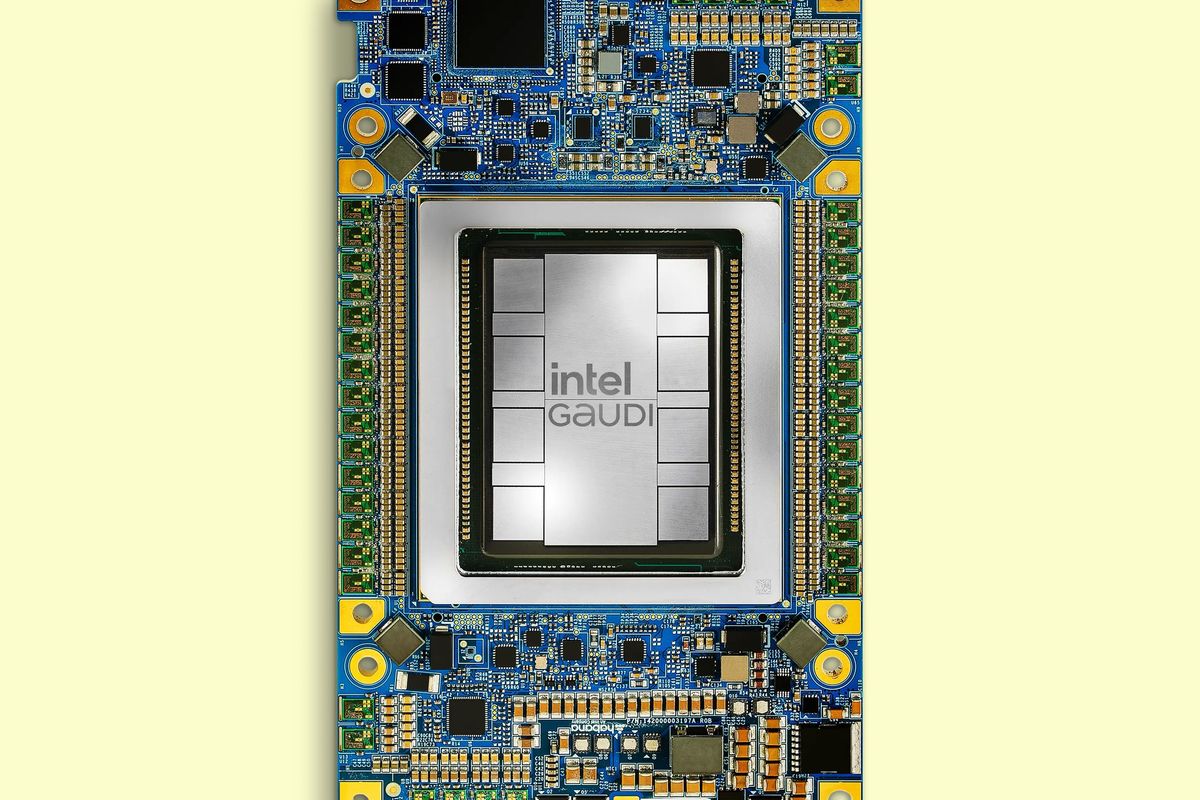
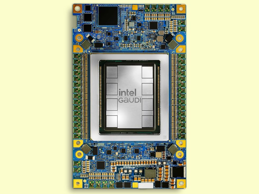


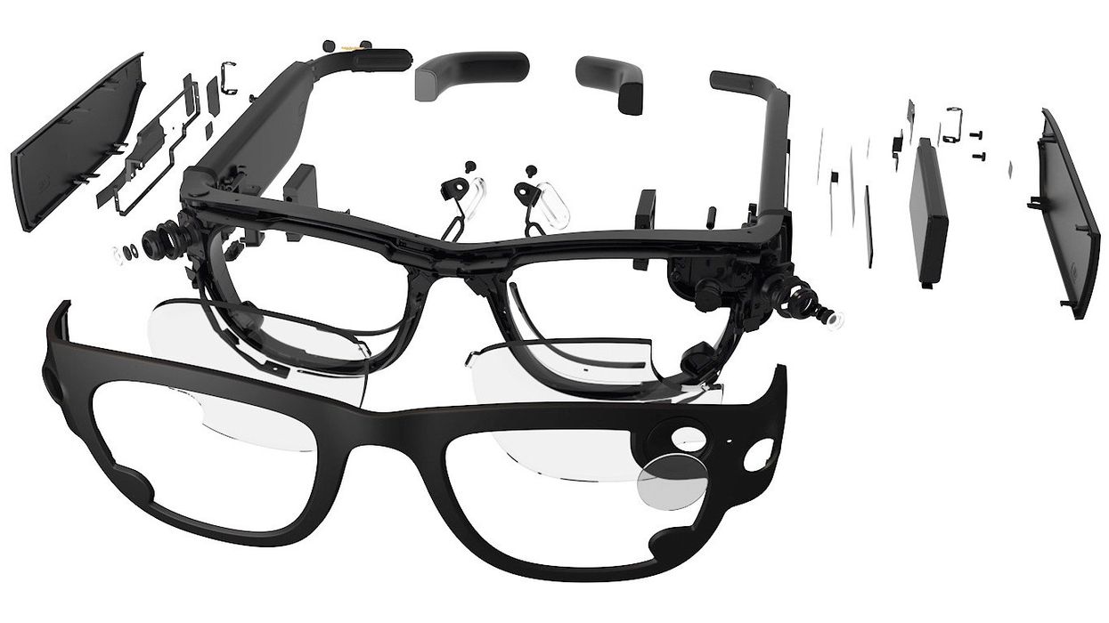
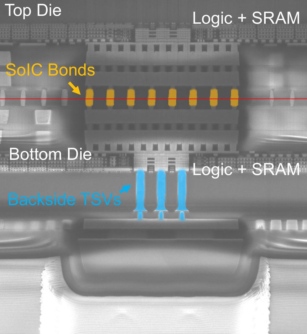 Meta’s prototype chip has both logic and memory on each silicon die. They’re bonded face-to-face, and through-silicon vias carry data and power to both.Meta
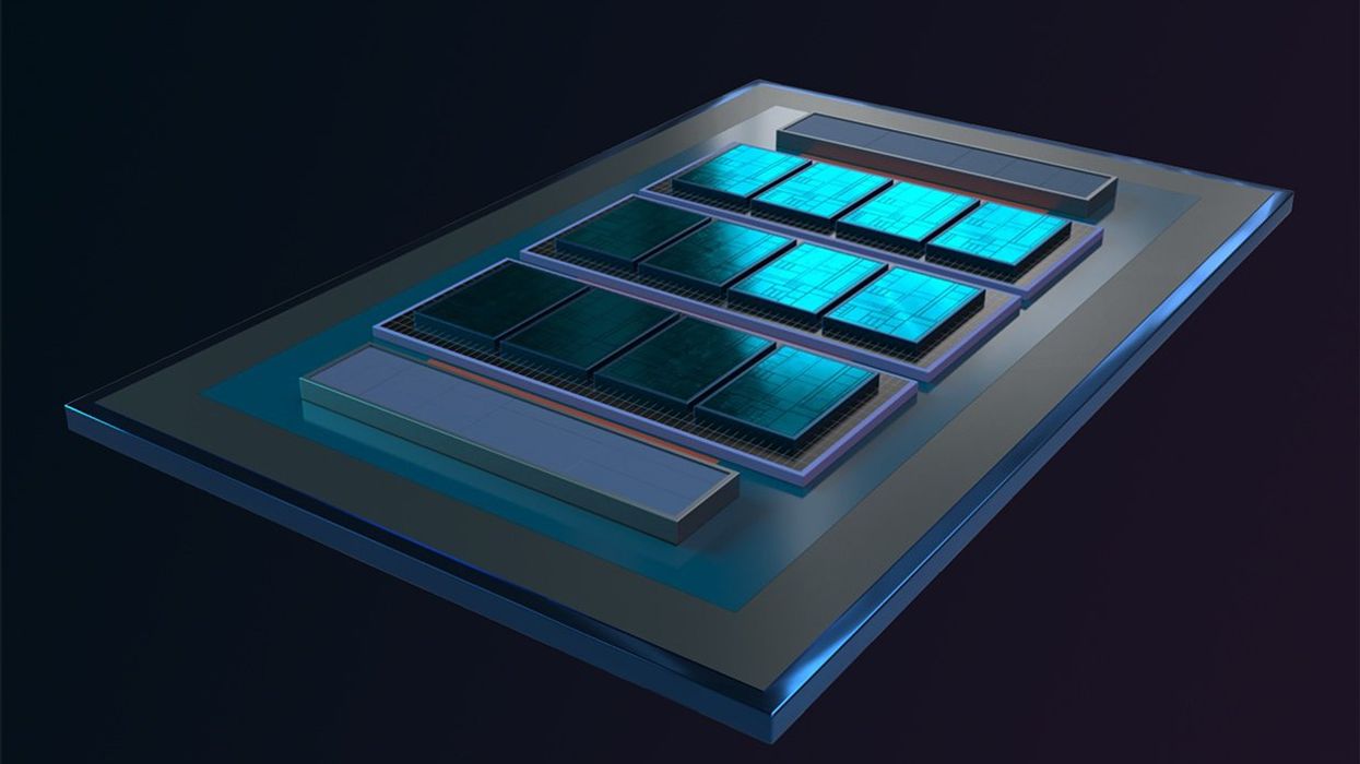
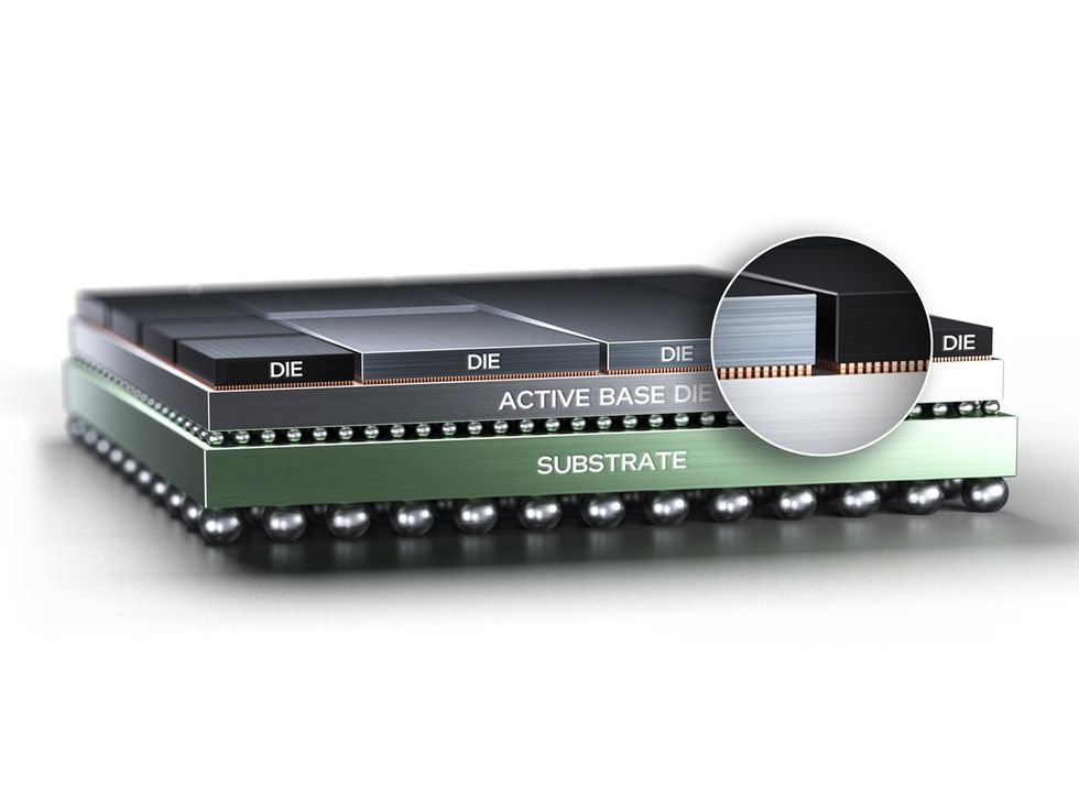 3D hybrid bonding links compute dies to base dies.Intel
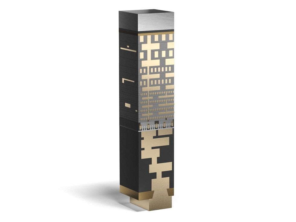 PowerVia puts the silicon’s power supply network below, leaving more room for data-carrying interconnects above.Intel
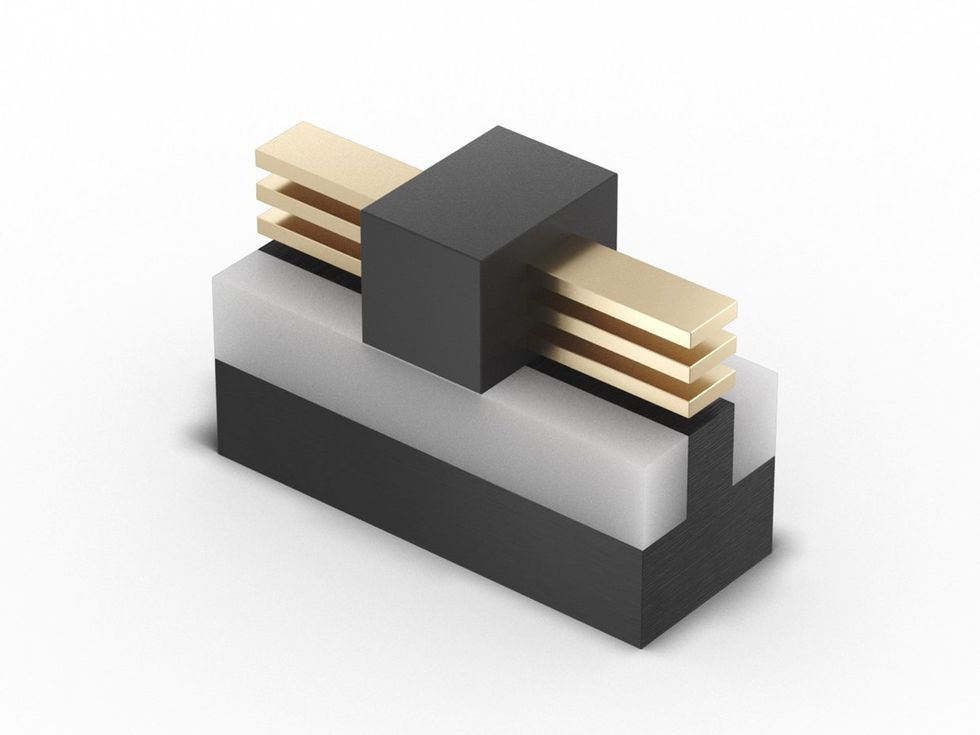 RibbonFET is Intel’s take on nanowire transistors.Intel
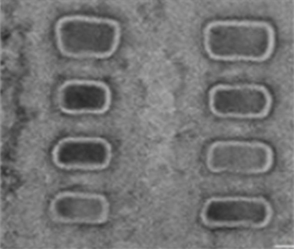 RibbonFET’s nanowires can have different widths depending on the needs of a logic cell.Intel
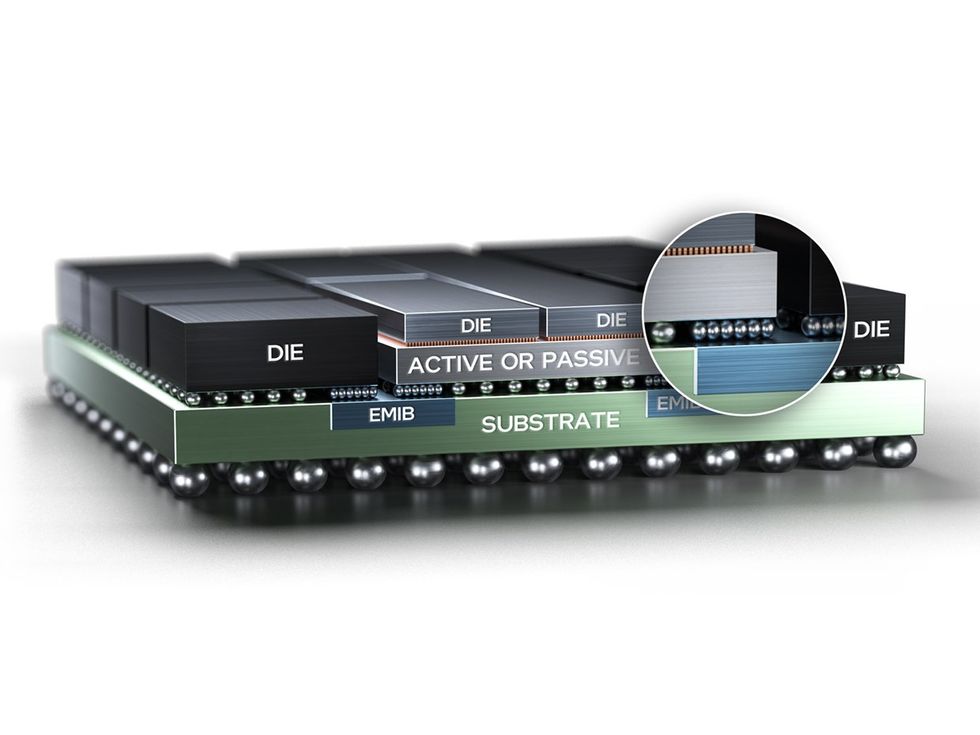 Dense 2D connections are formed by a small sliver of silicon called EMIB, which is embedded in the package substrate.Intel