Next-Gen Brain Implant Uses a Graphene Chip

A Barcelona-based startup called Inbrain Neuroelectronics has produced a novel brain implant made of graphene and is gearing up for its first in-human test this summer.
The technology is a type of brain-computer interface. BCIs have garnered interest because they record signals from the brain and transmit them to a computer for analysis. They have been used for medical diagnostics, as communication devices for people who can’t speak, and to control external equipment, including robotic limbs. But Inbrain intends to transform its BCI technology into a therapeutic tool for patients with neurological issues such as Parkinson’s disease.
Because Inbrain’s chip is made of graphene, the neural interface has some interesting properties, including the ability to be used to both record from and stimulate the brain. That bidirectionality comes from addressing a key problem with the metallic chips typically used in BCI technology: Faradaic reactions. Faradaic reactions are a particular type of electrochemical processes that occurs between a metal electrode and an electrolyte solution. As it so happens, neural tissue is largely composed of aqueous electrolytes. Over time, these Faradaic reactions reduce the effectiveness of the metallic chips.
That’s why Inbrain replaced the metals typically used in such chips with graphene, a material with great electrical conductivity. “Metals have Faraday reactions that actually make all the electrons interact with each other, degrading their effectiveness...for transmitting signals back to the brain,” said Carolina Aguilar, CEO and cofounder of Inbrain.
Because graphene is essentially carbon and not a metal, Aguilar says the chip can inject 200 times as much charge without creating a Faradic reaction. As a result, the material is stable over the millions of pulses of stimulation required of a therapeutic tool. While Inbrain is not yet testing the chip for brain stimulation, the company expects to reach that goal in due time.
The graphene-based chip is produced on a wafer using traditional semiconductor technology, according to Aguilar. At clean-room facilities, Inbrain fabricates a 10-micrometer-thick chip. The chip consists of what Aguilar terms “graphene dots” (not to be confused with graphene quantum dots) that range in size from 25 to 300 micrometers. “This micrometer scale allows us to get that unique resolution on the decoding of the signals from the brain, and also provides us with the micrometric stimulation or modulation of the brain,” added Aguilar.
Testing the Graphene-Based BCI
The first test of the platform in a human patient will soon be performed at the University of Manchester, in England, where it will serve as an interface during the resection of a brain tumor. When resecting a tumor, surgeons must ensure that they don’t damage areas like the brain’s language centers so the patient isn’t impaired after the surgery. “The chip is positioned during the tumor resection so that it can read, at a very high resolution, the signals that tell the surgeon where there is a tumor and where there is not a tumor,” says Aguilar. That should enable the surgeons to extract the tumor with micrometric precision while preserving functional areas like speech and cognition.
Aguilar added, “We have taken this approach for our first human test because it is a very reliable and quick path to prove the safety of graphene, but also demonstrate the potential of what it can do in comparison to metal technology that is used today.”
Aguilar stresses that the Inbrain team has already tested the graphene-based chip’s biocompatibility. “We have been working for the last three years in biocompatibility through various safety studies in large animals,” said Aguilar. “So now we can have these green lights to prove an additional level of safety with humans.”
While this test of the chip at Manchester is aimed at aiding in brain tumor surgery, the same technology could eventually be used to help Parkinson’s patients. Toward this aim, Inbrain’s system was granted Breakthrough Device Designation last September from the U.S. Food & Drug Administration as an adjunctive therapy for treating Parkinson’s disease. “For Parkinson’s treatment, we have been working on different preclinical studies that have shown reasonable proof of superiority versus current commercial technology in the [reduction] of Parkinson’s disease symptoms,” said Aguilar.
For treating Parkinson’s, Inbrain’s chip connects with the nigrostriatal pathway in the brain that is critical for movements. The chip will first decode the intention message from the brain that triggers a step or the lifting of the arm—something that a typical BCI can do. But Inbrain’s chip, with its micrometric precision, can also decode pathological biomarkers related to Parkinson’s symptoms, such as tremors, rigidity, and freezing of the gait.
By determining these biomarkers with great precision, Inbrain’s technology can determine how well a patient’s current drug regimen is working. In this first iteration of the Inbrain chip, it doesn’t treat the symptoms of Parkinson’s directly, but instead makes it possible to better target and reduce the amount of drugs that are used in treatment.
“Parkinson’s patients take huge amounts of drugs that have to be changed over time just to keep up with the growing resistance patients develop to the power of the drug,” said Aguilar. “We can reduce it at least 50 percent and hopefully in the future more as our devices become precise.”


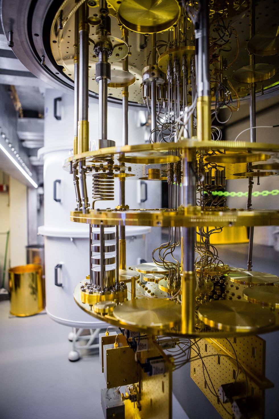 Superconducting qubits are measured at temperatures as low as 20 millikelvin in a dilution refrigerator.Nathan Fiske/MIT