FreshRSS

Zobrazení pro čtení

Jsou dostupné nové články, klikněte pro obnovení stránky.

NVIDIA Scoops Up Wins at COMPUTEX Best Choice Awards

Od: Melody Tu

Building on more than a dozen years of stacking wins at the COMPUTEX trade show’s annual Best Choice Awards, NVIDIA was today honored with BCAs for its latest technologies.

The NVIDIA GH200 Grace Hopper Superchip won the Computer and System Category Award; the NVIDIA Spectrum-X AI Ethernet networking platform won the Networking and Communication Category Award; and the NVIDIA AI Enterprise software platform won a Golden Award.

The awards — judged on the functionality, innovation and market potential of products exhibited at the leading computer and technology expo — were announced ahead of the show, which runs from June 4-7, in Taipei.

NVIDIA founder and CEO Jensen Huang will deliver a COMPUTEX keynote address on Sunday, June 2, at 7 p.m. Taiwan time, at the NTU Sports Center and online.

NVIDIA AI Enterprise Takes Gold

NVIDIA AI Enterprise — a cloud-native software platform that streamlines the development and deployment of copilots and other generative AI applications — won a Golden Award.

The platform lifts the burden of maintaining and securing complex AI software, so businesses can focus on building and harnessing the technology’s game-changing insights.

Microservices that come with NVIDIA AI Enterprise — including NVIDIA NIM and NVIDIA CUDA-X — optimize model performance and run anywhere with enterprise-grade security, support and stability, offering users a smooth transition from prototype to production.

Plus, the platform’s ability to improve AI performance results in better overall utilization of computing resources. This means companies using NVIDIA AI Enterprise need fewer servers to support the same workloads, greatly reducing their energy costs and data center footprint.

More BCA Wins for NVIDIA Technologies

NVIDIA GH200 and Spectrum-X were named best in their respective categories.

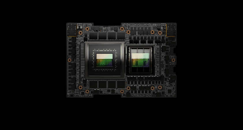
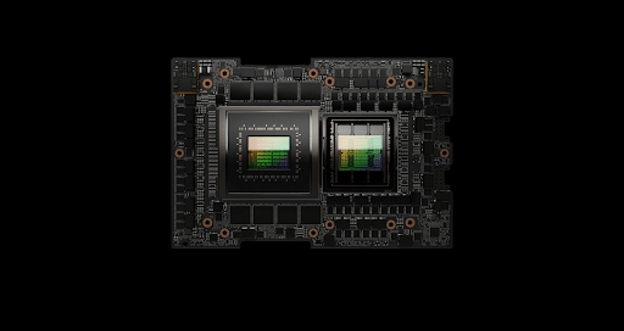
The NVIDIA GH200 Grace Hopper Superchip is the world’s first truly heterogeneous accelerated platform for AI and high-performance computing workloads. It combines the power-efficient NVIDIA Grace CPU with an NVIDIA Hopper architecture-based GPU over a high-bandwidth 900GB/s coherent NVIDIA NVLink chip-to-chip interconnect.

The superchip — shipping worldwide and powering more than 40 AI supercomputers across global research centers, system makers and cloud providers — supercharges scientific innovation with accelerated computing and scale-out solutions for AI inference, large language models, recommenders, vector databases, HPC applications and more.

The Spectrum-X platform, featuring NVIDIA Spectrum SN5600 switches and NVIDIA BlueField-3 SuperNICs, is the world’s first Ethernet fabric built for AI, accelerating generative AI network performance 1.6x over traditional Ethernet fabrics.

It can serve as the backend AI fabric for any AI cloud or large enterprise deployment, and is available from major server manufacturers as part of the full NVIDIA AI stack.

NVIDIA Partners Recognized

Other BCA winners include NVIDIA partners Acer, ASUS, MSI and YUAN, which were given Golden Awards for their respective laptops, gaming motherboards and smart-city applications — all powered by NVIDIA technologies, such as NVIDIA GeForce RTX 4090 GPUs, the NVIDIA Studio platform for creative workflows and the NVIDIA Jetson platform for edge AI and robotics.

ASUS also won a Computer and System Category Award, while MSI won a Gaming and Entertainment Category Award.

Learn more about the latest generative AI, HPC and networking technologies by joining NVIDIA at COMPUTEX.

Advanced Packaging Design For Heterogeneous Integration

Od: CP Hung

As device scaling slows down, a key system functional integration technology is emerging: heterogeneous integration (HI). It leverages advanced packaging technology to achieve higher functional density and lower cost per function. With the continuous development of major semiconductor applications such as AI HPC, edge AI and autonomous electrical vehicles, traditional chips are transforming into smaller, well-partitioned chiplets that require chip-to-chip interconnections to be denser, faster and more reliable. This boosts the demand for heterogeneous integration, elevating demand for innovative advanced packaging technologies.

HI uses advanced packaging to integrate chiplets with heterogeneous designs and process nodes into a single package. This allows enterprises to choose optimum process nodes for specific system demands, such as 3nm for computing chiplets, 7nm for radio frequency chiplets, or to quickly produce super chips with specific functions in a cost-effective manner. HI not only aims for higher interconnection density, but also integrates various functional components, such as logic chips, sensors, memory, and others, which are needed to complete the whole system in one package. Overall energy efficiency and performance is greatly improved, while package size can be significantly reduced.

Advanced packaging solutions for AI HPC

The typical high-density advanced package size for AI cloud computing processors is 55mm x 55mm or more, and contains a 5-2-5 (top 5 layers, middle 2 layers, bottom 5 layers) advanced substrate, or even up to 11-2-11 wiring layers. Chiplets can be interconnected by fan-out technology with silicon bridge or 2.5D with Si Interposer as the integration platform. Through this technique, industry aims to gain more computing power within the same space.

ASE provides high-density packaging solutions, including Flip Chip Ball Grid Array (FCBGA), Fan Out Chip-on-Substrate (FOCoS), FOCoS-Bridge and 2.5D. The chip-to-chip interconnections in FCBGA is accomplished through BGA substrate, and its minimum L/S (line width/line spacing) is only about 10μm/10μm. The very popular and in-demand CoWoS (Chip on Wafer on Substrate) is a 2.5D packaging technology that uses RDL (redistribution layer) on Si interposer to connect chiplets, and its L/S can be significantly reduced to 0.5μm/0.5μm.

In the Si interposer of a 2.5D package, all the chiplets are connected in a side-by-side arrangement, and as the required number of chiplets increases, its area becomes larger and larger, resulting in fewer and fewer Si interposer chips that can be made from each 12-inch wafer (generally less than 50). This indeed significantly increases the manufacturing cost of 2.5D packaging. However, not all applications require 0.5μm/0.5μm L/S, so ASE came up with FOCoS, which uses fan-out technology’s RDL to integrate different chiplets, and its L/S can reach 2μm/2μm. This gives alternative solutions to the market with lower costs. In addition, ASE’s FOCoS-Bridge technology uses silicon bridge to provide high-density routing for interconnecting different chips (such as logic chips and memory) in areas that require high-speed transmission and uses Fan-Out RDL to integrate in other areas. As such, it delivers both 0.5μm/0.5μm and 2μm/2μm flexibility in L/S design, while achieving a significant increase in packaging density and bandwidth.

High performance chip-package-system co-design

To achieve the aforementioned high bandwidth, the chip, package, and entire system must be designed together to achieve holistic design optimization instead of just considering the individual parts. When using electronic design automation (EDA) for design optimization, consideration must be given to overall signal change along the entire transmission path, including Cu pillar, RDL fine line, TSV, μbump, etc. Eye diagrams can then be used to analyze the SerDes link’s electrical performance. When designing differential pairs for high-speed signals, it is necessary to reduce return and insertion loss, especially in the operating frequency band. From chip to package to the entire system, Taiwan’s manufacturing advantage lies in the ability to accomplish the turnkey design process, from beginning to end.

Providing more computing power with less energy

The industry is currently focused on optimizing energy efficiency. One of the key questions being asked is whether the power regulation and decoupling components, which were previously located on the system board, can be moved closer to the package or processor chip. There is even talk of redesigning the on-chip power delivery network (PDN), including supplying power directly from the backside of the chip (Backside PDN).

Power integrity design for power delivery network (PDN)

Optimizing power integrity and minimizing noise can be achieved by strategically positioning the capacitor. Ideally, the capacitor should be placed as close to the chip as possible, but this is dependent on the capacitor’s size and the manufacturing process, both of which can impact cost and performance. Traditional surface-mount technology (SMT) capacitors are relatively large, but chip-level silicon capacitors (Si-Cap) are now available that offer decent capacitance values.

UCIe (Universal Chiplet Interconnect Express) Consortium

Traditionally, there are many standard communication protocols (such as Block-to-Block, Memory Bus, or Interconnection Interface Protocols) at the chip level and the board level for system designers. Industry protocols that specify package-level integration are growing, especially given the need for a universal interface for chiplet integration using 2.5D and FOCoS packaging technologies.

In March 2022, Intel invited upstream and downstream manufacturers in the semiconductor industry chain to form the UCIe Consortium, and a standardized data transmission architecture for chiplet integration was introduced to reduce the cost of advanced packaging design. ASE is proud to be a founding member (Promoter member).

ASE offers a diverse range of advanced packaging types. We have developed packaging design specifications that can be integrated with foundry solutions specifications as well as the system requirements of original equipment manufacturers (OEMs) and cloud service providers to create a comprehensive UCIe package standard. The standard can assist in realizing ubiquitous chiplet heterogeneous integration for HPC applications using various advanced packaging technology architectures, such as 2.5D, 3D, FOCoS, Fan-out, EMIB, CoWoS, etc. Headquartered in Taiwan, ASE is enthusiastically participating in the formulation of international standards and relentlessly providing integrated solutions to the global industry.

Heterogeneous integration has been in development for many years. It can be used to integrate not only homogeneous and heterogeneous chiplets but also other passive and active components including connectors, into a single package. Achieving this requires not only advanced packaging technologies but also design and testing coordination. ASE offers a comprehensive one-stop service solution that includes system design, packaging, and testing to help customers shorten chip design cycles and accelerate product innovation.

The post Advanced Packaging Design For Heterogeneous Integration appeared first on Semiconductor Engineering.

❌