FreshRSS

Zobrazení pro čtení

Jsou dostupné nové články, klikněte pro obnovení stránky.

3.5D: The Great Compromise

The semiconductor industry is converging on 3.5D as the next best option in advanced packaging, a hybrid approach that includes stacking logic chiplets and bonding them separately to a substrate shared by other components.

This assembly model satisfies the need for big increases in performance while sidestepping some of the thorniest issues in heterogeneous integration. It establishes a middle ground between 2.5D, which already is in widespread use inside of data centers, and full 3D-ICs, which the chip industry has been struggling to commercialize for the better part of a decade.

A 3.5D architecture offers several key advantages:

  • It creates enough physical separation to effectively address thermal dissipation and noise.
  • It provides a way to add more SRAM into high-speed designs. SRAM has been the go-to choice for processor cache since the mid-1960s, and remains an essential element for faster processing. But SRAM no longer scales at the same rate as digital transistors, so it is consuming more real estate (in percentage terms) at each new node. And because the size of a reticle is fixed, the best available option is to add area by stacking chiplets vertically.
  • By thinning the interface between processing elements and memory, a 3.5D approach also can shorten the distances that signals need to travel and greatly improve processing speeds well beyond a planar implementation. This is essential with large language models and AI/ML, where the amount of data that needs to be processed quickly is exploding.

Chipmakers still point to fully integrated 3D-ICs as the best performing alternative to a planar SoC, but packing everything into a 3D configuration makes it harder to deal with physical effects. Thermal dissipation is probably the most difficult to contend with. Workloads can vary significantly, creating dynamic thermal gradients and trapping heat in unexpected places, which in turn reduce the lifespan and reliability of chips. On top of that, power and substrate noise become more problematic at each new node, as do concerns about electromagnetic interference.

“What the market has adopted first is high-performance chips, and those produce a lot of heat,” said Marc Swinnen, director of product marketing at Ansys. “They have gone for expensive cooling systems with a huge number of fans and heat sinks, and they have opted for silicon interposers, which arguably are some of the most expensive technologies for connecting chips together. But it also gives the highest performance and is very good for thermal because it matches the coefficient of thermal expansion. Thermal is one of the big reasons that’s been successful. In addition to that, you may want bigger systems with more stuff that you can’t fit on one chip. That’s just a reticle-size limitation. Another is heterogeneous integration, where you want multiple different processes, like an RF process or the I/O, which don’t need to be in 5nm.”

A 3.5D assembly also provides more flexibility to add additional processor cores, and higher yield because known good die can be manufactured and tested separately, a concept first pioneered by Xilinx in 2011 at 28nm.

3.5D is a loose amalgamation of all these approaches. It can include two to three chiplets stacked on top of each other, or even multiple stacks laid out horizontally.

“It’s limited vertical, and not just for thermal reasons,” said Bill Chen, fellow and senior technical advisor at ASE Group. “It’s also for performance reasons. But thermal is the limiting factor, and we’ve talked about many different materials to help with that — diamond and graphene — but that limitation is still there.”

This is why the most likely combination, at least initially, will be processors stacked on SRAM, which simplifies the cooling. The heat generated by high utilization of different processing elements can be removed with heat sinks or liquid cooling. And with one or more thinned out substrates, signals will travel shorter distances, which in turn uses less power to move data back and forth between processors and memory.

“Most likely, this is going to be logic over memory on a logic process,” said Javier DeLaCruz, fellow and senior director of Silicon Ops Engineering at Arm. “These are all contained within an SoC normally, but a portion of that is going to be SRAM, which does not scale very well from node to node. So having logic over memory and a logic process is really the winning solution, and that’s one of the better use cases for 3D because that’s what really shortens your connectivity. A processor generally doesn’t talk to another processor. They talk to each other through memory, so having the memory on a different floor with no latency between them is pretty attractive.”

The SRAM doesn’t necessarily have to be at the same node as the processors advanced node, which also helps with yield, and reliability. At a recent Samsung Foundry event, Taejoong Song, the company’s vice president of foundry business development, showed a roadmap of a 3.5D configuration using a 2nm chiplet stacked on a 4nm chiplet next year, and a 1.4nm chiplet on top of a 2nm chiplet in 2027.


Fig. 1: Samsung’s heterogeneous integration roadmap showing stacked DRAM (HBM), chiplets and co-packaged optics. Source: Samsung Foundry

Intel Foundry’s approach is similar in many ways. “Our 3.5D technology is implemented on a substrate with silicon bridges,” said Kevin O’Buckley, senior vice president and general manager of Foundry Services at Intel. “This is not an incredibly costly, low-yielding, multi-reticle form-factor silicon, or even RDL. We’re using thin silicon slices in a much more cost-efficient fashion to enable that die-to-die connectivity — even stacked die-to-die connectivity — through a silicon bridge. So you get the same advantages of silicon density, the same SI (signal integrity) performance of that bridge without having to put a giant monolithic interposer underneath the whole thing, which is both cost- and capacity-prohibitive. It’s working. It’s in the lab and it’s running.”


Fig. 2: Intel’s 3.5D model. Source: Intel

The strategy here is partly evolutionary — 3.5D has been in R&D for at least several years — and part revolutionary, because thinning out the interconnect layer, figuring out a way to handle these thinner interconnect layers, and how to bond them is still a work in progress. There is a potential for warping, cracking, or other latent defects, and dynamically configuring data paths to maximize throughput is an ongoing challenge. But there have been significant advances in thermal management on two- and three-chiplet stacks.

“There will be multiple solutions,” said C.P. Hung, vice president of corporate R&D at ASE. “For example, besides the device itself and an external heat sink, a lot of people will be adding immersion cooling or local liquid cooling. So for the packaging, you can probably also expect to see the implementation of a vapor chamber, which will add a good interface from the device itself to an external heat sink. With all these challenges, we also need to target a different pitch. For example, nowadays you see mass production with a 45 to 40 pitch. That is a typical bumping solution. We expect the industry to move to a 25 to 20 micron bump pitch. Then, to go further, we need hybrid bonding, which is a less than 10 micron pitch.”


Fig. 3: Today’s interposers support more than 100,000 I/Os at a 45m pitch. Source: ASE

Hybrid bonding solves another thorny problem, which is co-planarity across thousands of micro-bumps. “People are starting to realize that the densities we’re interconnecting require a level of flatness, which the guys who make traditional things to be bonded are having a hard time meeting with reasonable yield,” David Fromm, COO at Promex Industries. “That makes it hard to build them, and the thinking is, ‘So maybe we’ve got to do something else.’ You’re starting to see some of that.”

Taming the Hydra
Managing heat remains a challenge, even with all the latest advances and a 3.5D assembly, but the ability to isolate the thermal effects from other components is the best option available today, and possibly well into the future. Still, there are other issues to contend with. Even 2.5D isn’t easy, and a large percentage of the 2.5D implementations have been bespoke designs by large systems companies with very deep pockets.

One of the big remaining challenges is closing timing so that signals arrive at the right place at the right fraction of a second. This becomes harder as more elements are added into chips, and in a 3.5D or 3D-IC, this can be incredibly complex.

“Timing ultimately is the key,” said Sutirtha Kabir, R&D director at Synopsys. “It’s not guaranteed that at whatever your temperature is, you can use the same library for timing. So the question is how much thermal- and IR-aware timing do you have to do? These are big systems. You have to make sure your sign-off is converging. There are two things coming out. There are a bunch of multi-physics effects that are all clumped together. And yes, you could traditionally do one at a time as sign-off, but that isn’t going to work very well. You need to figure out how to solve these problems simultaneously. Ultimately, you’re doing one design. It’s not one for thermal, one for IR, one for timing. The second thing is the data is exploding. How do you efficiently handle the data, because you cannot wait for days and days of runtime and simulation and analysis?”

Physically assembling these devices isn’t easy, either. “The challenge here is really in the thermal, electrical, and mechanical connection of all these various die with different thicknesses and different coefficients of thermal expansion,” said Intel’s O’Buckley. “So with three die, you’ve got the die and an active base, and those are substantially thinned to enable them to come together. And then EMIB is in the substrate. There’s always intense thermal-mechanical qualification work done to manage not just the assembly, but to ensure in the final assembly — the second-level assembly when this is going through system-level card attach — that this thing stays together.”

And depending upon demands for speed, the interconnects and interconnect materials can change. “Hybrid bonding gives you, by far, the best signal and power density,” said Arm’s DeLaCruz. “And it gives you the best thermal conductivity, because you don’t have that underfill that you would otherwise have to put in between the die, which is a pretty significant barrier. This is likely where the industry will go. It’s just a matter of having the production base.”

Hybrid bonding has been used for years for image sensors using wafer-on-wafer connections. “The tricky part is going into the logic space, where you’re moving from wafer-on-wafer to a die-on-wafer process, which is more complex,” DeLaCruz said. “While it currently would cost more, that’s a temporary problem because there’s not much of an installed base to support it and drive down the cost. There’s really no expensive material or equipment costs.”

Toward mass customization
All of this is leading toward the goal of choosing chiplets from a menu and then rapidly connecting them into some sort of architecture that is proven to work. That may not materialize for years. But commercial chiplets will show up in advanced designs over the next couple years, most likely in high-bandwidth memory with a customized processor in the stack, with more following that path in the future.

At least part of this will depend on how standardized the processes for designing, manufacturing, and testing become. “We’re seeing a lot of 2.5D from customers able to secure silicon interposers,” said Ruben Fuentes, vice president for the Design Center at Amkor Technology. “These customers want to place their chiplets on an interposer, then the full module is placed on a flip-chip substrate package. We also have customers who say they either don’t want to use a silicon interposer or cannot secure them. They prefer an RDL interconnect with S-SWIFT or with S-Connect, which serves as an interposer in very dense areas.”

But with at least a third of these leading designs only for internal use, and the remainder confined to large processor vendors, the rest of the market hasn’t caught up yet. Once it does, that will drive economies of scale and open the door to more complete assembly design kits, commercial chiplets, and more options for customization.

“Everybody is generally going in the same direction,” said Fuentes. “But not everything is the same height. HBMs are pre-packaged and are taller than ICs. HBMs could have 12 or 16 ICs stacked inside. It makes a difference from a co-planarity and thermal standpoint, and metal balancing on different layers. So now vendors are having a hard time processing all this data because suddenly you have these huge databases that are a lot bigger than the standard packaging databases. We’re seeing bridges, S-Connect, SWIFT, and then S-SWIFT. This is new territory, and we’re seeing a performance gap in the packaging tools. There’s work that needs to be done here, but software vendors have been very proactive in finding solutions. Additionally, these packages need to be routed. There is limited automated routing, so a good amount of interactive routing is still required, so it takes a lot of time.”


Fig. 4: Packaging roadmap showing bridge and hybrid bonding connections for modules and chiplets, respectively. Source: Amkor Technology

What’s missing
The key challenges ahead for 3.5D are proven reliability and customizability — requirements that are seemingly contradictory, and which are beyond the control of any single company. There are four major pieces to making all of this work.

EDA is the first important piece of the puzzle, and the challenge extends just beyond a single chip. “The IC designers have to think about a lot of things concurrently, like thermal, signal integrity, and power integrity,” said Keith Lanier, technical product management director at Synopsys. “But even beyond that, there’s a new paradigm in terms of how people need to work. Traditional packaging folks and IC designers need to work closely together to make these 3.5D designs successful.”

It’s not just about doing more with the same or fewer people. It’s doing more with different people, too. “It’s understanding the architecture definition, the functional requirements, constraints, and having those well-defined,” Lanier said. “But then it’s also feasibility, which includes partitioning and technology selection, and then prototyping and floor-planning. This is lots and lots of data that is required to be generated, and you need analysis-driven exploration, design, and implementation. And AI will be required to help designers and system design teams manage the sheer complexity of these 3.5D designs.”

Process/assembly design kits are a second critical piece, and this is likely to be split between the foundries and the OSATs. “If the customer wants a silicon interposer for a 2.5D package, it would be up to the foundry that’s going to manufacture the interposer to provide the PDK. We would provide the PDK for all of our products, such as S-SWIFT and S-Connect,” said Amkor’s Fuentes.

Setting realistic parameters is the third piece of the puzzle. While the type of processing elements and some of the analog functions may change — particularly those involving power and communication — most of the components will remain the same. That determines what can be pre-built and pre-tested, and the speed and ease of assembly.

“A lot of the standards that are being deployed, like UCIe interfaces and HBM interfaces are heading to where 20% is customization and 80% is on the shelf,” said Intel’s O’Buckley. “But we aren’t there today. At the scale that our customers are deploying these products, the economics of spending that extra time to optimize an implementation is a decimal point. It’s not leveraging 80/20 standards. We’ll get there. But most of these designs you can count on your fingers and toes because of the cost and scale required to do them. And until the infrastructure for standards-based chiplets gets mature, the barrier of entry for companies that want to do this without that scale is just too high. Still, it is going to happen.”

Ensuring processes are consistent is the fourth piece of the puzzle. The tools and the individual processes don’t need to change. “The customer has a ‘target’ for the outcome they want for a particular tool, which typically is a critical dimension measured by a metrology tool,” said David Park, vice president of marketing at Tignis. “As long as there is some ‘measurement’ that determines the goodness of some outcome, which typically is the result of a process step, we can either predict the bad outcome — and engineers have to take some corrective or preventive action — or we can optimize the recipe of that tool in real time to keep the result in the range they want.”

Park noted there is a recipe that controls the inputs. “The tool does whatever it is supposed to do,” he said. “Then you measure the output to see how far you deviated from the acceptable output.”

The challenge is that inside of a 3.5D system, what is considered acceptable output is still being defined. There are many processes with different tolerances. Defining what is consistent enough will require a broad understanding of how all the pieces work together under specific workloads, and where the potential weaknesses are that need to be adjusted.

“One of the problems here is as these densities get higher and the copper pillars get smaller, the amount of space you need between the pillar and the substrate have to be highly controlled,” said Dick Otte, president and CEO of Promex. “There’s a conflict — not so much with how you fabricate the chip, because it usually has the copper pillars on it — but with the substrate. A lot of the substrate technologies are not inherently flat. It’s the same issue with glass. You’ve got a really nice flat piece of glass. The first thing you’re going to do is put down a layer of metal and you’re going to pattern it. And then you put down a layer of dielectric, and suddenly you’ve got a lump where the conductor goes. And now, where do you put the contact points? So you always have the one plan which is going to be the contact point where all the pillars come in. But what if I only need one layer and I don’t need three?”

Conclusion
For the past decade, the chip industry has been trying to figure out a way to balance faster processing, domain-specific designs, limited reticle size, and the enormous cost of scaling an SoC. After investigating nearly every possible packaging approach, interconnect, power delivery method, substrate and dielectric material, 3.5D has emerged as the front runner — at least for now.

This approach provides the chip industry with a common thread on which to begin developing assembly design kits, commercial chiplets, and to fill in the missing tools and services throughout the supply chain. Whether this ultimately becomes a springboard for full 3D-ICs, or a platform on which to use 3D stacking more effectively, remains to be seen. But for the foreseeable future, large chipmakers have converged on a path forward to provide orders of magnitude performance improvements and a way to contain costs. The rest of the industry will be working to smooth out that path for years to come.

Related Reading
Intel Vs. Samsung Vs. TSMC
Foundry competition heats up in three dimensions and with novel technologies as planar scaling benefits diminish.
3D Metrology Meets Its Match In 3D Chips And Packages
Next-generation tools take on precision challenges in three dimensions.
Design Flow Challenged By 3D-IC Process, Thermal Variation
Rethinking traditional workflows by shifting left can help solve persistent problems caused by process and thermal variations.
Floor-Planning Evolves Into The Chiplet Era
Automatically mitigating thermal issues becomes a top priority in heterogeneous designs.

The post 3.5D: The Great Compromise appeared first on Semiconductor Engineering.

Heterogeneity Of 3DICs As A Security Vulnerability

A new technical paper titled “Harnessing Heterogeneity for Targeted Attacks on 3-D ICs” was published by Drexel University.

Abstract
“As 3-D integrated circuits (ICs) increasingly pervade the microelectronics industry, the integration of heterogeneous components presents a unique challenge from a security perspective. To this end, an attack on a victim die of a multi-tiered heterogeneous 3-D IC is proposed and evaluated. By utilizing on-chip inductive circuits and transistors with low voltage threshold (LVT), a die based on CMOS technology is proposed that includes a sensor to monitor the electromagnetic (EM) emissions from the normal function of a victim die, without requiring physical probing. The adversarial circuit is self-powered through the use of thermocouples that supply the generated current to circuits that sense EM emissions. Therefore, the integration of disparate technologies in a single 3-D circuit allows for a stealthy, wireless, and non-invasive side-channel attack. A thin-film thermo-electric generator (TEG) is developed that produces a 115 mV voltage source, which is amplified 5 × through a voltage booster to provide power to the adversarial circuit. An on-chip inductor is also developed as a component of a sensing array, which detects changes to the magnetic field induced by the computational activity of the victim die. In addition, the challenges associated with detecting and mitigating such attacks are discussed, highlighting the limitations of existing security mechanisms in addressing the multifaceted nature of vulnerabilities due to the heterogeneity of 3-D ICs.”

Find the technical paper here. Published June 2024.

Alec Aversa and Ioannis Savidis. 2024. Harnessing Heterogeneity for Targeted Attacks on 3-D ICs. In Proceedings of the Great Lakes Symposium on VLSI 2024 (GLSVLSI ’24). Association for Computing Machinery, New York, NY, USA, 246–251. https://doi.org/10.1145/3649476.3660385.

The post Heterogeneity Of 3DICs As A Security Vulnerability appeared first on Semiconductor Engineering.

Powering Next-Generation Insightful Design

The Ansys team is gearing up for an exciting time at DAC this week, where we’ll be sharing a whole new way of visualizing physical phenomena in 3D-IC designs, powered by NVIDIA Omniverse, a platform for developing OpenUSD and RTX-enabled 3D applications and workflows. Please attend our Exhibitor Forum session so we can show you the valuable design insights you can gain by interactively viewing surface currents, temperatures and mechanical deformations in a representative 3D-IC design.

Visualizing physical phenomena in 3D is a new paradigm for IC packaging signal and power integrity (SI/PI) engineers who are more familiar with schematics and 2D results plots (TDR, eye diagrams, SYZ parameters, etc). There’s a good reason for that – it really hasn’t been practical to save 3D physics data – or even to run full 3D simulations – for complex IC package designs until more recent (~5-10 years) advancements in Ansys solver technologies along with increasing accessibility to high performance compute power. I have had the pleasure of supporting a few early adopters in the SI/PI engineering community as they used 3D field plotting in HFSS to gain design insights that helped them avoid costly tape-out delays and chip re-spin. Their experiences motivate my desire to share this invaluable capability with the greater IC packaging design community.

I started my career using HFSS to design antennas for biomedical applications. Like me, the greater antenna and RF component design community has been plotting fields in 3D from Day 1 – I don’t know of any antenna engineer that hasn’t plotted a 3D radiation pattern after running an HFSS simulation. What I do know is that I’ve met hundreds of SI/PI engineers who have never plotted surface currents in their package or PCB models after running an HFSS simulation. And that must change.

…but why exactly? What value does one gain by plotting fields in 3D? If you don’t know what kind of design insights you gain by plotting fields, please allow me to show you because seeing is revealing.

Let’s say I send a signal from point A and it reflects off 3 different plates before returning back to point A:

Fig. 1: The plot below shows the received power from a sensor placed at Point A (the same position as the emitter). Can you tell which bump in this two 2D plot is the original signal returned back home?

Fig. 2: No? Neither can I. Even if you somehow guessed correctly, could you explain what caused all those other bumps with certainty?

With HFSS field plotting, everything becomes crystal clear:

Video 1: 3-bounce animation.

The original signal returns after a travel distance of 6 meters around the circle while the rest of the bumps result from other reflections – this is the kind of physical insight that a 2D plot simply can’t deliver.

Advanced packaging for 3D-IC design can’t be done with generic rules of thumb. To meet stringent specifications (operate at higher frequencies, speeds, and lower latency, power consumption), engineers are demanding the use of HFSS because its gold-standard reputation has come from countless validation studies comparing simulated results against measurement, and there is no room to compromise on accuracy for these very complex and costly designs. As more electronics are packed into tighter spaces, the risk for unwanted coupling between the different components (often stacked vertically) increases and being able to identify the true aggressors becomes more challenging. That’s when field visualization as a means to debug – i.e., uncover, learn, truly understand – what’s happening becomes an invaluable tool.

What exactly is causing unwanted radiation or reflections? What exactly is the source of noise coupling into this line? Are we seeing any current crowding on conductors or significant volume losses in dielectrics that may lead to thermal problems? Plot the fields and you will have the information required to diagnose issues and design the exact right solution – nothing more (over-designed), nothing less (failing design).

If you’re one of the early adopters who has plotted fields in highly complex designs, you will know that fields post-processing can be very graphics intensive – especially if you want to immerse yourself in the physical phenomena taking place in your design by plotting in a full 3D volume and cutting through the 3D space layer by layer. Ansys uses the enhanced graphics and visual rendering capabilities offered by NVIDIA Omniverse core technologies, available as APIs, to provide a seamlessly interactive and more intuitive experience, increasing accessibility to design insights that engineers can only gain by physics visualization.

I’m not asking my SI/PI engineering colleagues to ditch the schematics and 2D results plots – I just believe that they should (and inevitably will!) add 3D field plotting into their design process. The rise in design complexity coupled with advancements in Ansys and NVIDIA technologies is poised to make 3D field plotting – an invaluable yet heretofore underutilized tool in the world of signal and power integrity design – a practical requirement. For a first look into what will one day be commonplace design practice, please attend our Exhibitor Forum session on Wed., June 26, 1:45 PM -3:00 PM at DAC to experience our interactive demonstration of Ansys physics visualization in a representative 3D-IC design, powered by NVIDIA Omniverse.

The post Powering Next-Generation Insightful Design appeared first on Semiconductor Engineering.

U.S. Proposes Restrictions On Tech Investments In China

The U.S. proposed new regulations to curtail American investments in Chinese technologies that pose a national security threat, specifically calling out semiconductors and microelectronics, quantum information technologies, and AI.

The draft regulations come nearly a year after the Biden administration issued an executive order prohibiting investments in sensitive technologies used to accelerate China’s military technologies.  “This proposed rule advances our national security by preventing the many benefits certain U.S. investments provide — beyond just capital — from supporting the development of sensitive technologies in countries that may use them to threaten our national security,” said Paul Rosen, assistant secretary of the treasury for investment security, in a release.

Prohibited Semiconductor Transactions

The 165-page proposal defines prohibited semiconductor transactions (pages 133-134), which include:

  • EDA software for the design of ICs or advanced packaging;
  • Front-end semiconductor fab equipment designed for performing the volume fabrication of ICs, including equipment used in the production stages from a blank wafer or substrate to a completed wafer or substrate;
  • Equipment for performing volume advanced packaging;
  • Commodity, material, software, or technology designed exclusively for use in or with EUV lithography equipment;
  • Design of ICs for operation at or below 4.5 Kelvin, and ICs that meet or exceed performance criteria in Export Control Classification Number 3A090;
  • Fabrication of logic ICs using a non-planar transistor architecture, or with a production technology node of 16/14 nanometers or less, including FD-SOI ICs;
  • Fabrication of NAND with 128 layers or more, or DRAM ICs at 18nm half-pitch or less;
  • Fabrication of gallium-based compound semiconductors, or ICs using graphene transistors or carbon nanotubes, and
  • Any IC using advanced packaging techniques.


Prohibited AI And Supercomputing Transactions

Prohibited transactions for supercomputers and artificial intelligence (pages 134-135) include:

  • Any supercomputer enabled by advanced ICs that can provide a theoretical compute capacity of 100 or more double-precision (64-bit) petaflops, or 200 or more single-precision (32-bit) petaflops of processing power within a 41,600 cubic foot or smaller envelope;
  • Any quantum computer, or production of any of the critical components required to produce a quantum computer, such as a dilution refrigerator or two-stage pulse tube cryocooler;
  • Quantum sensing platforms for military, government or mass-surveillance end use;
  • Quantum network or quantum communication system, and
  • AI for military end use, weapons targeting, target identification, and military decision-making.

Written comments are due by Aug. 4, 2024. The regulations are expected to be finalized this calendar year.

More Reading:
Chip Industry Week In Review
GF, BAE team up; $2B Czech SiC plant; SEMI’s capacity report; imec’s CFETs, beamforming transmitters; Germany chip plant postponed; EUV patterning advances; interconnect metals; plasma etch.

The post U.S. Proposes Restrictions On Tech Investments In China appeared first on Semiconductor Engineering.

Controlling Warpage In Advanced Packages

Warpage is becoming a serious concern in advanced packaging, where a heterogeneous mix of materials can cause uneven stress points during assembly and packaging, and under real workloads in the field.

Warpage plays a critical role in determining whether an advanced package can be assembled successfully and meet long-term reliability targets. New advances, such as molding compounds with improved thermal properties, advanced modeling techniques, and creative architectures involving two molding steps are enabling greater control over package warpage, while also providing more flexibility to optimize a robust multi-chiplet system.

Warpage is the inevitable result of the mismatch in coefficients of thermal expansion (CTEs) between the silicon chip, molding compound, copper, polyimide, and other materials. It changes throughout the assembly process, and can cause cracking or delamination failures. The most vulnerable spots include low-k cores, which are subject to cracking and shorts, or non-wet failures in micro-bumps.

“One thing that’s very hot these days is the discussion around warpage and stress of the package,” said Kenneth Larsen, senior director of product management at Synopsys. “This is not only when you’re going through the manufacturing process, where you change temperatures. That can cause warpage. But it’s also when the device you’re building needs to be inserted into a socket. You can have issues around warpage there, as well.”

Even when warpage is effectively addressed during assembly and packaging, a device still may warp under heavy usage in the field. This is particularly true with heterogeneous designs, where chiplets are developed using different materials or processes, and where logic is concentrated in specific areas of an asymmetrical package.

The transition to multi-chiplet packaging is accelerating rapidly due to demands for ever-higher processing speeds and low latency, especially in mobile, automotive and high-performance compute/AI applications. Engineers increasingly are turning to modeling and simulation to understand temperature-dependent warpage, which can vary depending on die thickness, mold-to-silicon ratio, and substrate type. Organic substrates are very attractive because they are inexpensive and can be customized to any size, but they are much more flexible and susceptible to warpage than silicon substrates.

All these considerations point to the need for thermal and structural models of complex heterogeneous assemblies and packages. “Advanced modeling allows companies to simulate the behavior of different materials, thermal dynamics, and mechanical stresses during the assembly process,” said Mike Kelly, vice president of chiplets/FCBGA integration at Amkor. “Through this virtual experimentation, one can predict and mitigate potential challenges, ensuring that the final product meets stringent quality and reliability standards.”

How warpage happens
The assembly process includes multiple heating and cooling steps, which induce a certain amount of deformation between adjacent materials with different thermal and mechanical properties. In advanced packaging, warpage in the 100 micron range is not unheard of.

One of the reasons warpage is such a problem today is the large size of chiplets and the very tight process windows for chiplets, redistribution layers (RDLs), substrates, and bumps of various sizes. The relative expansion and contraction of neighboring materials depends on differences in the material’s CTE, which spells out the increase in size with each degree change of temperature (ppm/°C).

“Chiplets are typically relatively large die,” said Dick Otte, CEO of Promex Industries. “In the iPad, it’s 20 x 30 millimeters, with as many as 10,000 I/Os — usually copper pillar. Just simply taking a single die and putting it down on a substrate can be quite a challenge because the pitches are so small. So what’s critical for these assemblies is controlling warpage and planarity. It needs to stay planar through the whole reflow solder process to bridge that gap between the copper pillar and the contact on the circuit board without warping.”

Warpage can either happen upward, bending at the edges (smiling), or downward (crying), depending on the relative CTEs of the materials in the stack. Silicon, for example, is 2.8; copper is 17; FR4 PCB is 14 to 17 ppm/°C. The worst CTE mismatch is between a silicon interposer and an organic substrate.

It helps to envision stacks in packaging as groups of materials. “You have to look at the CTE of the materials and their reaction at temperatures, so you’ve got relatively low expansion copper on the top and solder at the bottom,” Otte said. “They’re kind of equal with a high expansion dielectric in the middle, so that when you heat this thing up, it kind of expands by the same amount. If you just put all the copper on the top, that thing is going to warp toward the copper side when you heat it up. Copper is 15 ppm per degree C. The organics are more like twice that, at 25 to 30 ppm/°C.

Other key metrics are the modulus, or the elasticity of a material, and the glass transition temperature (Tg), the temperature at which a material begins to flow. These values are related, too. For example, when it comes to the thermal behavior of polymers like epoxy molding compound (EMC), the modulus tends to plummet above its glass transition temperature. That happens because polymer chains tend to slide freely in the liquid state, whereas they are stiffer in a solid form.

In addition to solder reflow, warpage tends to occur at the post-molding curing step. Hung-Chun Yang and colleagues at ASE recently determined that die thickness substantially influences warpage levels measured at multiple steps in an existing process for chip-first fan-out chip on substrate package. [1] They noted that “severe wafer warpage occurred after curing, resulting in misalignment and difficulty in handling in the subsequent process.” To reduce package warpage, the team replaced a metal carrier/thin film approach with a glass carrier. The team also determined that a 3D finite element method (FEM) captures the warpage behavior and agreed well with actual test vehicle data.


Fig. 1: The glass carrier in the improved flow (right) induced less warpage than the original flow. Increasing the die thickness also dramatically reduced warpage. Source: ASE

The chip-first process begins with probing the fabricated wafers, thinning and then electroplating copper studs prior to sawing and placement of known good die in two schemes. The initial process used a metal carrier that is removed after molding and replaced with a thin film. The improved process uses a glass carrier that remained through molding, curing, mold grinding, RDL, and copper pillar processes, and then wass de-bonded.

Warpage reaches its maximum level during post-mold curing, and it changes most dramatically at the curing step and after glass carrier debonding. The glass carrier flow reduces warpage overall. In addition, the ASE engineers determined they can reduce warpage an additional 35% by increasing the wafer thickness from 0.54mm to 0.7mm.

A second strategy for reducing warpage involves using EMCs with different thermal properties, especially when the process calls for two molding steps. Amkor engineers recently evaluated the reliability performance of two high-performance multi-chiplet packages by modeling and fabricating two high-performance test vehicles. One used a module approximately the size of one reticle, containing 1 ASIC, 2 HBMs and 2 bridge die (33 x 26mm). The second module was 3 reticles in size, with 2 ASICs, 8 HBMs and 10 bridge dies (54 x 46mm). [2] Heejun Jang and colleagues at Amkor Technology Korea carried out modeling and simulation using the Ansys Parametric Design Language (APDL) version 16.1 simulator and compared results with test vehicles containing dummy dies.

Amkor’s die-last S-Connect process starts with a carrier wafer, on which copper studs for the bridge die and copper pillars are fabricated (see figure 2). The integrated passives and bridge die are embedded in the first mold, which is cured and then ground back. RDL is deposited on the mold and solder capture pads and dies attached to the pads using micro-bumps. Then, the solder is reflowed and underfilled. The second mold around the face-up die is cured and ground back, followed by C4 bumping on the bottom for flip-chip connect to the substrate. The simulation analyzes warpage with 9 combinations of 3 different EMCs with high, medium, and low CTEs (7 to 12 ppm below Tg, 22 to 46 ppm above Tg) and high-to-low glass transition temperatures (145°C to 175°C). [2]


Fig. 2: Process flow for S-Connect Package. Source: Amkor

Warpage as a function of EMC choice showed all materials followed the same smile pattern at room temperature, and cry pattern at high temperature (250°C). The EMCs with the lower CTEs caused less warpage. And in cases where the mold occupies more area relative to chip area, the warpage level is more pronounced. More importantly, the warpage levels were roughly 50% higher for 450µm die relative to 650µm-thick die. Interestingly, the thicker silicon die was 3X more effective in controlling warpage relative to EMC material selection on overall module warpage, so die thickness is the biggest lever in reducing warpage in cases where it can be increased.

Reliability testing is paramount once the package configuration is chosen. Amkor ran its advanced packaging test vehicles through moisture resistance testing, highly accelerated stress testing, thermal cycling condition B, and high temperature storage tests. These are needed to root out infant mortality issues, and cross-sectional analysis can reveal any cracks or latent defects that could precipitate into failures in field use.

While the above example may constitute a large multi-chiplet package today, package sizes are growing larger still, which means even more attention to warpage will be needed. More and more this will drive assembly lines toward digital twin or virtual representations to enable process and package optimization.

“By creating virtual representations of the semiconductor assembly line, one can identify potential areas of concern and optimize control strategies,” said Amkor’s Kelly. “Virtual fabrication in package assembly enables companies to assess the impact of design changes on manufacturing processes before physical prototypes are even created. This not only accelerates the product development cycle, but also minimizes the risk of costly errors.”

The early identification of potential bottlenecks further shortens cycle times, and enhances overall efficiency.

Conclusion
Going forward, even greater attention to mechanical and thermal properties will be required by teams comprised of designers and packaging engineers. “Tight tolerances in new packaging design require an accurate analysis of mechanical and electrical tolerances during stack up,” said Curtis Zwenger, vice president of engineering and technical marketing at Amkor. “Increasingly higher levels of process capability are required, with common metrics like CpK. Identification of these critical interactions in the design can be accomplished early in process development with this type of modeling. In turn, these analyses guide the investment of advanced process control to ensure process capability is maintained.”

References

  1. C. Yang, et al, “Investigation of Wafer Warpage Evolution Based on Fan-out Chip-first Process,” 2024 International Conference on Electronics Packaging (ICEP), Toyama, Japan, 2024, pp. 151-152, doi: 10.23919/ICEP61562.2024.10535572.
  2. H. Jang et al., “Reliability Performance of S-Connect Module (Bridge Technology) for Heterogeneous Integration Packaging,” 2023 IEEE 73rd Electronic Components and Technology Conference (ECTC), Orlando, FL, USA, 2023, pp. 1027-1031, doi: 10.1109/ECTC51909.2023.00175.

Related Reading
What Works Best For Chiplets
Not all chiplets are interchangeable, and options will be limited.

The post Controlling Warpage In Advanced Packages appeared first on Semiconductor Engineering.

Power Electronic Packaging for Discrete Dies

A technical paper titled “Substrate Embedded Power Electronics Packaging for Silicon Carbide MOSFETs” was published by researchers at University of Cambridge, University of Warwick, Chongqing University, and SpaceX.

Abstract:

“This paper proposes a new power electronic packaging for discrete dies, namely Standard Cell which consists of a step-etched active metal brazed (AMB) substrate and a flexible printed circuit board (flex-PCB). The standard cell exhibits high thermal conductivity, complete electrical insulation, and low stray inductance, thereby enhancing the performance of SiC MOSFET devices. The standard cell has a stray power loop inductance of less than 1 nH and a gate loop inductance of less than 1.5 nH . The standard cell has a flat body with surface-mounting electrical connections on one side and direct thermal connections on the other. The use of flex-PCB die interconnection enables maximum utilization of source pads while providing a flexible gate-source connection and the converter PCB. This paper presents the design concept of the standard cell and experimentally validates its effectiveness in a converter system.”

Find the technical paper here. Published May 2024.

A. Janabi et al., “Substrate Embedded Power Electronics Packaging for Silicon Carbide MOSFETs,” in IEEE Transactions on Power Electronics, doi: 10.1109/TPEL.2024.3396779.

Related Reading
Big Shifts In Power Electronics Packaging
Packages are becoming more complex to endure high power, high temperature conditions across a variety of applications.
Power Semiconductors: A Deep Dive Into Materials, Manufacturing & Business
Premium Content: How these devices are made and work, challenges in manufacturing, related startups, as well as the reasons why so much effort and resources are being spent to develop new materials, and new processes.</

The post Power Electronic Packaging for Discrete Dies appeared first on Semiconductor Engineering.

Adoption of Chiplet Technology in the Automotive Industry

A technical paper titled “Chiplets on Wheels: Review Paper on Holistic Chiplet Solutions for Autonomous Vehicles” was published by researchers at the Indian Institute of Technology, Madras.

Abstract
“On the advent of the slow death of Moore’s law, the silicon industry is moving towards a new era of chiplets. The automotive industry is experiencing a profound transformation towards software-defined vehicles, fueled by the surging demand for automotive compute chips, expected to reach 20-22 billion by 2030. High-performance compute (HPC) chips become instrumental in meeting the soaring demand for computational power. Various strategies, including centralized electrical and electronic architecture and the innovative Chiplet Systems, are under exploration. The latter, breaking down System-on-Chips (SoCs) into functional units, offers unparalleled customization and integration possibilities. The research accentuates the crucial open Chiplet ecosystem, fostering collaboration and enhancing supply chain resilience. In this paper, we address the unique challenges that arise when attempting to leverage chiplet-based architecture to design a holistic silicon solution for the automotive industry. We propose a throughput-oriented micro-architecture for ADAS and infotainment systems alongside a novel methodology to evaluate chiplet architectures. Further, we develop in-house simulation tools leveraging the gem5 framework to simulate latency and throughput. Finally, we perform an extensive design of thermally-aware chiplet placement and develop a micro-fluids-based cooling design.”

Find the technical paper here. Published May 2024.

Narashiman, Swathi, Divyaratna Joshi, Deepak Sridhar, Harish Rajesh, Sanjay Sattva, and Varun Manjunath. “Chiplets on Wheels: Review Paper on Holistic Chiplet Solutions for Autonomous Vehicles.” arXiv preprint arXiv:2406.00182 (2024).

The post Adoption of Chiplet Technology in the Automotive Industry appeared first on Semiconductor Engineering.

Hybrid Bonding Plays Starring Role in 3D Chips


Chipmakers continue to claw for every spare nanometer to continue scaling down circuits, but a technology involving things that are much bigger—hundreds or thousands of nanometers across—could be just as significant over the next five years.

Called hybrid bonding, that technology stacks two or more chips atop one another in the same package. That allows chipmakers to increase the number of transistors in their processors and memories despite a general slowdown in the shrinking of transistors, which once drove Moore’s Law. At the IEEE Electronic Components and Technology Conference (ECTC) this past May in Denver, research groups from around the world unveiled a variety of hard-fought improvements to the technology, with a few showing results that could lead to a record density of connections between 3D stacked chips: some 7 million links per square millimeter of silicon.

All those connections are needed because of the new nature of progress in semiconductors, Intel’s Yi Shi told engineers at ECTC. Moore’s Law is now governed by a concept called system technology co-optimization, or STCO, whereby a chip’s functions, such as cache memory, input/output, and logic, are fabricated separately using the best manufacturing technology for each. Hybrid bonding and other advanced packaging tech can then be used to assemble these subsystems so that they work every bit as well as a single piece of silicon. But that can happen only when there’s a high density of connections that can shuttle bits between the separate pieces of silicon with little delay or energy consumption.

Out of all the advanced-packaging technologies, hybrid bonding provides the highest density of vertical connections. Consequently, it is the fastest growing segment of the advanced-packaging industry, says Gabriella Pereira, technology and market analyst at Yole Group. The overall market is set to more than triple to US $38 billion by 2029, according to Yole, which projects that hybrid bonding will make up about half the market by then, although today it’s just a small portion.

In hybrid bonding, copper pads are built on the top face of each chip. The copper is surrounded by insulation, usually silicon oxide, and the pads themselves are slightly recessed from the surface of the insulation. After the oxide is chemically modified, the two chips are then pressed together face-to-face, so that the recessed pads on each align. This sandwich is then slowly heated, causing the copper to expand across the gap and fuse, connecting the two chips.

Making Hybrid Bonding Better


An illustration showing how to make hybrid bonding better
  1. Hybrid bonding starts with two wafers or a chip and a wafer facing each other. The mating surfaces are covered in oxide insulation and slightly recessed copper pads connected to the chips’ interconnect layers.
  2. The wafers are pressed together to form an initial bond between the oxides.
  3. The stacked wafers are then heated slowly, strongly linking the oxides and expanding the copper to form an electrical connection.
  1. To form more secure bonds, engineers are flattening the last few nanometers of oxide. Even slight bulges or warping can break dense connections.
  2. The copper must be recessed from the surface of the oxide just the right amount. Too much and it will fail to form a connection. Too little and it will push the wafers apart. Researchers are working on ways to control the level of copper down to single atomic layers.
  3. The initial links between the wafers are weak hydrogen bonds. After annealing, the links are strong covalent bonds [below]. Researchers expect that using different types of surfaces, such as silicon carbonitride, which has more locations to form chemical bonds, will lead to stronger links between the wafers.
  4. The final step in hybrid bonding can take hours and require high temperatures. Researchers hope to lower the temperature and shorten the process time.
  5. Although the copper from both wafers presses together to form an electrical connection, the metal’s grain boundaries generally do not cross from one side to the other. Researchers are trying to cause large single grains of copper to form across the boundary to improve conductance and stability.

Hybrid bonding can either attach individual chips of one size to a wafer full of chips of a larger size or bond two full wafers of chips of the same size. Thanks in part to its use in camera chips, the latter process is more mature than the former, Pereira says. For example, engineers at the European microelectronics-research institute Imec have created some of the most dense wafer-on-wafer bonds ever, with a bond-to-bond distance (or pitch) of just 400 nanometers. But Imec managed only a 2-micrometer pitch for chip-on-wafer bonding.

The latter is a huge improvement over the advanced 3D chips in production today, which have connections about 9 μm apart. And it’s an even bigger leap over the predecessor technology: “microbumps” of solder, which have pitches in the tens of micrometers.

“With the equipment available, it’s easier to align wafer to wafer than chip to wafer. Most processes for microelectronics are made for [full] wafers,” says Jean-Charles Souriau, scientific leader in integration and packaging at the French research organization CEA Leti. But it’s chip-on-wafer (or die-to-wafer) that’s making a splash in high-end processors such as those from AMD, where the technique is used to assemble compute cores and cache memory in its advanced CPUs and AI accelerators.

In pushing for tighter and tighter pitches for both scenarios, researchers are focused on making surfaces flatter, getting bound wafers to stick together better, and cutting the time and complexity of the whole process. Getting it right could revolutionize how chips are designed.

WoW, Those Are Some Tight Pitches

The recent wafer-on-wafer (WoW) research that achieved the tightest pitches—from 360 nm to 500 nm—involved a lot of effort on one thing: flatness. To bond two wafers together with 100-nm-level accuracy, the whole wafer has to be nearly perfectly flat. If it’s bowed or warped to the slightest degree, whole sections won’t connect.

Flattening wafers is the job of a process called chemical mechanical planarization, or CMP. It’s essential to chipmaking generally, especially for producing the layers of interconnects above the transistors.

“CMP is a key parameter we have to control for hybrid bonding,” says Souriau. The results presented at ECTC show CMP being taken to another level, not just flattening across the wafer but reducing mere nanometers of roundness on the insulation between the copper pads to ensure better connections.

“It’s difficult to say what the limit will be. Things are moving very fast.” —Jean-Charles Souriau, CEA Leti

Other researchers focused on ensuring those flattened parts stick together strongly enough. They did so by experimenting with different surface materials such as silicon carbonitride instead of silicon oxide and by using different schemes to chemically activate the surface. Initially, when wafers or dies are pressed together, they are held in place with relatively weak hydrogen bonds, and the concern is whether everything will stay in place during further processing steps. After attachment, wafers and chips are then heated slowly, in a process called annealing, to form stronger chemical bonds. Just how strong these bonds are—and even how to figure that out—was the subject of much of the research presented at ECTC.

Part of that final bond strength comes from the copper connections. The annealing step expands the copper across the gap to form a conductive bridge. Controlling the size of that gap is key, explains Samsung’s Seung Ho Hahn. Too little expansion, and the copper won’t fuse. Too much, and the wafers will be pushed apart. It’s a matter of nanometers, and Hahn reported research on a new chemical process that he hopes to use to get it just right by etching away the copper a single atomic layer at a time.

The quality of the connection counts, too. The metals in chip interconnects are not a single crystal; instead they’re made up of many grains, crystals oriented in different directions. Even after the copper expands, the metal’s grain boundaries often don’t cross from one side to another. Such a crossing should reduce a connection’s electrical resistance and boost its reliability. Researchers at Tohoku University in Japan reported a new metallurgical scheme that could finally generate large, single grains of copper that cross the boundary. “This is a drastic change,” says Takafumi Fukushima, an associate professor at Tohoku. “We are now analyzing what underlies it.”

Other experiments discussed at ECTC focused on streamlining the bonding process. Several sought to reduce the annealing temperature needed to form bonds—typically around 300 °C—as to minimize any risk of damage to the chips from the prolonged heating. Researchers from Applied Materials presented progress on a method to radically reduce the time needed for annealing—from hours to just 5 minutes.

CoWs That Are Outstanding in the Field

A series of gray-scale images of the corner of an object at increasing magnification. Imec used plasma etching to dice up chips and give them chamfered corners. The technique relieves mechanical stress that could interfere with bonding.Imec

Chip-on-wafer (CoW) hybrid bonding is more useful to makers of advanced CPUs and GPUs at the moment: It allows chipmakers to stack chiplets of different sizes and to test each chip before it’s bound to another, ensuring that they aren’t dooming an expensive CPU with a single flawed part.

But CoW comes with all of the difficulties of WoW and fewer of the options to alleviate them. For example, CMP is designed to flatten wafers, not individual dies. Once dies have been cut from their source wafer and tested, there’s less that can be done to improve their readiness for bonding.

Nevertheless, researchers at Intel reported CoW hybrid bonds with a 3-μm pitch, and, as mentioned, a team at Imec managed 2 μm, largely by making the transferred dies very flat while they were still attached to the wafer and keeping them extra clean throughout the process. Both groups used plasma etching to dice up the dies instead of the usual method, which uses a specialized blade. Unlike a blade, plasma etching doesn’t lead to chipping at the edges, which creates debris that could interfere with connections. It also allowed the Imec group to shape the die, making chamfered corners that relieve mechanical stress that could break connections.

CoW hybrid bonding is going to be critical to the future of high-bandwidth memory (HBM), according to several researchers at ECTC. HBM is a stack of DRAM dies—currently 8 to 12 dies high—atop a control-logic chip. Often placed within the same package as high-end GPUs, HBM is crucial to handling the tsunami of data needed to run large language models like ChatGPT. Today, HBM dies are stacked using microbump technology, so there are tiny balls of solder surrounded by an organic filler between each layer.

But with AI pushing memory demand even higher, DRAM makers want to stack 20 layers or more in HBM chips. The volume that microbumps take up means that these stacks will soon be too tall to fit properly in the package with GPUs. Hybrid bonding would shrink the height of HBMs and also make it easier to remove excess heat from the package, because there would be less thermal resistance between its layers.

“I think it’s possible to make a more-than-20-layer stack using this technology.” —Hyeonmin Lee, Samsung

At ECTC, Samsung engineers showed that hybrid bonding could yield a 16-layer HBM stack. “I think it’s possible to make a more-than-20-layer stack using this technology,” says Hyeonmin Lee, a senior engineer at Samsung. Other new CoW technology could also help bring hybrid bonding to high-bandwidth memory. Researchers at CEA Leti are exploring what’s known as self-alignment technology, says Souriau. That would help ensure good CoW connections using just chemical processes. Some parts of each surface would be made hydrophobic and some hydrophilic, resulting in surfaces that would slide into place automatically.

At ECTC, researchers from Tohoku University and Yamaha Robotics reported work on a similar scheme, using the surface tension of water to align 5-μm pads on experimental DRAM chips with better than 50-nm accuracy.

The Bounds of Hybrid Bonding

Researchers will almost certainly keep reducing the pitch of hybrid-bonding connections. A 200-nm WoW pitch is not just possible but desirable, Han-Jong Chia, a project manager for pathfinding systems at Taiwan Semiconductor Manufacturing Co. , told engineers at ECTC. Within two years, TSMC plans to introduce a technology called backside power delivery. (Intel plans the same for the end of this year.) That’s a technology that puts the chip’s chunky power-delivery interconnects below the surface of the silicon instead of above it. With those power conduits out of the way, the uppermost levels can connect better to smaller hybrid-bonding bond pads, TSMC researchers calculate. Backside power delivery with 200-nm bond pads would cut down the capacitance of 3D connections so much that a measure of energy efficiency and signal speed would be as much as eight times better than what can be achieved with 400-nm bond pads.

Black squares dot most of the top of an orange metallic disc. Chip-on-wafer hybrid bonding is more useful than wafer-on-wafer bonding, in that it can place dies of one size onto a wafer of larger dies. However, the density of connections that can be achieved is lower than for wafer-on-wafer bonding.Imec

At some point in the future, if bond pitches narrow even further, Chia suggests, it might become practical to “fold” blocks of circuitry so they are built across two wafers. That way some of what are now long connections within the block might be able to take a vertical shortcut, potentially speeding computations and lowering power consumption.

And hybrid bonding may not be limited to silicon. “Today there is a lot of development in silicon-to-silicon wafers, but we are also looking to do hybrid bonding between gallium nitride and silicon wafers and glass wafers…everything on everything,” says CEA Leti’s Souriau. His organization even presented research on hybrid bonding for quantum-computing chips, which involves aligning and bonding superconducting niobium instead of copper.

“It’s difficult to say what the limit will be,” Souriau says. “Things are moving very fast.”

This article was updated on 11 August 2024.

This article appears in the September 2024 print issue as “The Copper Connection.”

Comparing Thermal Properties In Molybdenum Substrate To Si And Glass For A System-On-Foil Integration (RIT, Lux)

A technical paper titled “Comparative Analysis of Thermal Properties in Molybdenum Substrate to Silicon and Glass for a System-on-Foil Integration” was published by researchers at Rochester Institute of Technology and Lux Semiconductors.

Abstract:

“Advanced electronics technology is moving towards smaller footprints and higher computational power. In order to achieve this, advanced packaging techniques are currently being considered, including organic, glass, and semiconductor-based substrates that allow for 2.5D or 3D integration of chips and devices. Metal-core substrates are a new alternative with similar properties to those of semiconductor-based substrates but with the added benefits of higher flexibility and metal ductility. This work comprehensively compares the thermal properties of a novel metal-based substrate, molybdenum, and silicon and fused silica glass substrates in the context of system-on-foil (SoF) integration. A simple electronic technique is used to simulate the heat generated by a typical CPU and to measure the heat dissipation properties of the substrates. The results indicate that molybdenum and silicon are able to effectively dissipate a continuous power density of 2.3 W/mm2 as the surface temperature only increases by ~15°C. In contrast, the surface temperature of fused silica glass substrates increases by >140°C for the same applied power. These simple techniques and measurements were validated with infrared camera measurements as well as through finite element analysis via COMSOL simulation. The results validate the use of molybdenum as an advanced packaging substrate and can be used to characterize new substrates and approaches for advanced packaging.”

Find the technical paper here. Published May 2024.

Huang, Tzu-Jung, Tobias Kiebala, Paul Suflita, Chad Moore, Graeme Housser, Shane McMahon, and Ivan Puchades. 2024. “Comparative Analysis of Thermal Properties in Molybdenum Substrate to Silicon and Glass for a System-on-Foil Integration” Electronics 13, no. 10: 1818. https://doi.org/10.3390/electronics13101818

Related Reading
The Race To Glass Substrates
Replacing silicon and organic substrates requires huge shifts in manufacturing, creating challenges that will take years to iron out.


The post Comparing Thermal Properties In Molybdenum Substrate To Si And Glass For A System-On-Foil Integration (RIT, Lux) appeared first on Semiconductor Engineering.

Expect a Wave of Wafer-Scale Computers


At TSMC’s North American Technology Symposium on Wednesday, the company detailed both its semiconductor technology and chip-packaging technology road maps. While the former is key to keeping the traditional part of Moore’s Law going, the latter could accelerate a trend toward processors made from more and more silicon, leading quickly to systems the size of a full silicon wafer. Such a system, Tesla’s next generation Dojo training tile is already in production, TSMC says. And in 2027 the foundry plans to offer technology for more complex wafer-scale systems than Tesla’s that could deliver 40 times as much computing power as today’s systems.

For decades chipmakers increased the density of logic on processors largely by scaling down the area that transistors take up and the size of interconnects. But that scheme has been running out of steam for a while now. Instead, the industry is turning to advanced packaging technology that allows a single processor to be made from a larger amount of silicon. The size of a single chip is hemmed in by the largest pattern that lithography equipment can make. Called the reticle limit, that’s currently about 800 square millimeters. So if you want more silicon in your GPU you need to make it from two or more dies. The key is connecting those dies so that signals can go from one to the other as quickly and with as little energy as if they were all one big piece of silicon.

TSMC already makes a wafer-size AI accelerator for Cerebras, but that arrangement appears to be unique and is different from what TSMC is now offering with what it calls System-on-Wafer.

In 2027, you will get a full-wafer integration that delivers 40 times as much compute power, more than 40 reticles’ worth of silicon, and room for more than 60 high-bandwidth memory chips, TSMC predicts

For Cerebras, TSMC makes a wafer full of identical arrays of AI cores that are smaller than the reticle limit. It connects these arrays across the “scribe lines,” the areas between dies that are usually left blank, so the wafer can be diced up into chips. No chipmaking process is perfect, so there are always flawed parts on every wafer. But Cerebras designed in enough redundancy that it doesn’t matter to the finished computer.

However, with its first round of System-on-Wafer, TSMC is offering a different solution to the problems of both reticle limit and yield. It starts with already tested logic dies to minimize defects. (Tesla’s Dojo contains a 5-by-5 grid of pretested processors.) These are placed on a carrier wafer, and the blank spots between the dies are filled in. Then a layer of high-density interconnects is constructed to connect the logic using TSMC’s integrated fan-out technology. The aim is to make data bandwidth among the dies so high that they effectively act like a single large chip.

By 2027, TSMC plans to offer wafer-scale integration based on its more advanced packaging technology, chip-on-wafer-on-substrate (CoWoS). In that technology, pretested logic and, importantly, high-bandwidth memory, is attached to a silicon substrate that’s been patterned with high-density interconnects and shot through with vertical connections called through-silicon vias. The attached logic chips can also take advantage of the company’s 3D-chip technology called system-on-integrated chips (SoIC).

The wafer-scale version of CoWoS is the logical endpoint of an expansion of the packaging technology that’s already visible in top-end GPUs. Nvidia’s next GPU, Blackwell, uses CoWos to integrate more than 3 reticle sizes’ worth of silicon, including 8 high-bandwidth memory (HBM) chips. By 2026, the company plans to expand that to 5.5 reticles, including 12 HBMs. TSMC says that would translate to more than 3.5 times as much compute power as its 2023 tech allows. But in 2027, you can get a full wafer integration that delivers 40 times as much compute, more than 40 reticles’ worth of silicon and room for more than 60 HBMs, TSMC predicts.

What Wafer Scale Is Good For

The 2027 version of system-on-wafer somewhat resembles technology called Silicon-Interconnect Fabric, or Si-IF, developed at UCLA more than five years ago. The team behind SiIF includes electrical and computer-engineering professor Puneet Gupta and IEEE Fellow Subramanian Iyer, who is now charged with implementing the packaging portion of the United States’ CHIPS Act.

Since then, they’ve been working to make the interconnects on the wafer more dense and to add other features to the technology. “If you want this as a full technology infrastructure, it needs to do many other things beyond just providing fine-pitch connectivity,” says Gupta, also an IEEE Fellow. “One of the biggest pain points for these large systems is going to be delivering power.” So the UCLA team is working on ways to add good-quality capacitors and inductors to the silicon substrate and integrating gallium nitride power transistors.

AI training is the obvious first application for wafer-scale technology, but it is not the only one, and it may not even be the best, says University of Illinois Urbana-Champaign computer architect and IEEE Fellow Rakesh Kumar. At the International Symposium on Computer Architecture in June, his team is presenting a design for a wafer-scale network switch for data centers. Such a system could cut the number of advanced network switches in a very large—16,000-rack—data center from 4,608 to just 48, the researchers report. A much smaller, enterprise-scale, data center for say 8,000 servers could get by using a single wafer-scale switch.

Electromigration Concerns Grow In Advanced Packages

The incessant demand for more speed in chips requires forcing more energy through ever-smaller devices, increasing current density and threatening long-term chip reliability. While this problem is well understood, it’s becoming more difficult to contain in leading-edge designs.

Of particular concern is electromigration, which is becoming more troublesome in advanced packages with multiple chiplets, where various bonding and interconnect schemes create abrupt changes in materials and geometries. For example, electrons may travel from a copper trace to a solder bump of SAC (tin-silver-copper), then to an underbump metal based on nickel, and finally to an interposer copper pad. That, in turn, can cause atoms to shift, resulting in failures in solder joints or in copper redistribution layers in high-density fan-out packages.

“From an electromigration perspective, advanced packaging causes increased packaging density, reduced packaging size, and the dimensions of interconnects to shrink, so the current density is now in close proximity to the maximum current density limit per EM design rules,” said Dermott Lynch, director of technical product management in Synopsys‘ EDA Group.

Any additional stresses the package may be subjected to during assembly and use, whether mechanical or thermal, also can help induce or accelerate electromigration. “Electromigration, in general, gets worse due to temperature and stress, both of which advanced packaging increases,” said Lynch. “Electromigration is also cumulative, so essentially it integrates all the temperature highs and stress over the lifetime until an interconnect breaks down or shorts. Larger processing temperature and operation temperature will make it worse, but it also depends on time under that temperature.”

In fact, managing thermal pathways is perhaps the greatest challenge associated the movement toward the ultimate package, a 3D-IC. “Electromigration is very temperature-sensitive,” said Marc Swinnen, director of product marketing in Ansys’ Semiconductor Division. “Depending on your thermal map, your power integrity will have to adapt to the local temperature profile that you have. So when you look at a chip, you can calculate how much power the chip is putting out, but you cannot tell how hot the chip will get because ‘it depends.’ Is it sitting on a cold plate or sitting in the sun in the Sahara? System concerns come in, and multi-physics modeling is important to understanding these co-dependent effects.”

Thermal engineering also means moving heat away from the most vulnerable points of failure, such as solder bumps. “Effective thermal management is essential for bump reliability,” said Curtis Zwenger, vice president of engineering and technical marketing at Amkor. “Engineers are incorporating thermal enhancement techniques, such as the use of thermal interface materials and advanced heat dissipation solutions, to ensure that bumps are not subjected to excessive temperature-related stresses.”

Zwenger noted that engineers are looking into new materials, while optimizing the use of existing materials to minimize the possibility of electromigration. “Semiconductor packaging engineers are implementing a range of measures to enhance bump reliability and maximize bump yield. These strategies include new materials for solder bumps and underbump metallization, optimizing bump size, pitch and shape for reliability, advanced process control methods to control variability and maximize yield, and simulating and modeling reliability.”

What is electromigration?
Electromigration is the mass transport of metal atoms caused by the electron wind from current flowing through a conductor, typically copper. When current density is high enough, metal will diffuse in the direction of current flow, creating tiny hillocks downstream and leaving behind vacancies or voids. With enough electromigration, failures occur due to severe line thinning, causing opens, or due to hillocks that bridge adjacent lines, causing short circuits.

Electromigration is a diffusion-controlled mechanism that can take three forms — bulk, grain boundary, or surface diffusion, depending on the metal. Aluminum migrates by grain boundary diffusion whereas copper migrates on the surface or at its grain boundaries.

For most of the semiconductor industry’s history, electromigration was primarily an on-chip concern, but on-chip EM is largely under control by reliability engineers. But with the scaling and rapid developments in advanced packaging — implementing TSVs, fan-out packaging with redistribution layers, and copper pillar bumps — electromigration has emerged as a major threat at the package level. Current flowing through the solder bump causes joule heating, and heat from other parts of the package may also dissipate through the solder bumps. EM can become an issue for solder joint connections between chip and interposer, or chip and PCB, as well as in RDLs. Solder joint failures typically manifest as voids or cracks.

Fig. 1: Electromigration can create short circuits between two interconnects through the development of hillocks, or an open circuit through the creation of voids in interconnect. Source: Ansys

Fig. 1: Electromigration can create short circuits between two interconnects through the development of hillocks, or an open circuit through the creation of voids in interconnect. Source: Ansys

Electromigration progresses more quickly at higher temperatures, at higher currents, under greater mechanical stress and in the presence of defects or impurities in the metal. Black’s equation describes an interconnect’s mean time-to-failure with respect to its temperature, current density and the activation energy needed to dislodge a metal atom as:

Black's equation

J is the current density, k is Boltzmann’s constant, T is temperature, Ea is the activation energy, and N is a scaling factor that depends on the metal’s properties. Black’s equation is useful because it easily shows how shorter, wider interconnects will tend to have longer MTTF. In addition, electromigration time-to-failure very strongly depends on the interconnect’s temperature. That temperature is primarily the result of the chip’s environmental temperature, self-heating of the conductor caused by current flow, the heat from neighboring interconnects or transistors, and the thermal conductivity of the surrounding material.

It is also important to note that electromigration is a runaway process. As current density and/or temperature increases, electromigration increases, which raises current density, causing more metal to migrate in a destructive feedback loop.

EM failure modes and allowable current density
In the case of copper redistribution layers in polyimide material, as current flows through the RDL, heat accumulates in the conductor due to Joule heating generation, which can degrade performance. As the required current density and Joule heating temperature is increasing in the fine-line Cu RDL structures (<5nm lines and spaces), self-heating is considered a key factor in the reliability of high-density fan out packages.

JiHye Kwon, senior manager of R&D at Amkor, recently used EM testing and Black’s equation to determine the electromigration failure mechanisms for a given RDL stack and high-density fan-out package with 2µm or 10µm wide RDL layers, 1,000µm long. [1]

High density fan-out is an emerging technology, as it features more aggressive scaling than wafer level fan-out packages. The three layers of copper RDL (3µm thick with Ta/Cu seed) were fabricated followed by polyimide fill, copper pillar deposition, die attach, and overmold. Kwon’s team tested both 2 and 10µm RDL at different current densities and temperatures until resistance increased by 100% (EM failure), but the maximum allowed current density corresponded with a 20% resistance increase. The failure modes occurred in two stages, first by void nucleation and growth and second with copper reduction and oxidation. The study yielded Ea and current density exponent values that can be useful in future designs of RDLs.

Meanwhile, a team of researchers from ASE recently demonstrated how susceptibility to electromigration is determined on copper pillar interconnects in flip chip quad flat no-lead (FCQFN) for high-power automotive applications. The multi-layered copper pillar bumps with a Cu/Ni/Sn1.8Ag configuration were bonded to a silver-plated copper leadframe and tested under extreme EM conditions of 10 kA/cm2 current density and temperatures of 150°C, 160°C and 180°C, while taking in-situ resistance measurements. [2] The EM failures corresponded with rapid rises in electrical resistance that corresponded with the formation of intermetallic compounds and voids at the Cu/solder interfaces. The team built an EM prediction model of interconnects based on a Black-type EM equation, following the JEDEC standard with five test conditions.

After the statistic calculation from the lifetime of samples, the ASE team determined activation energy of Cu pillar interconnects in the FCQFN package (1.12 ± 0.03 eV). The maximum current of the Cu pillar interconnects allowable lasting 10 years at a 105°C operating temperature at a 0.1% failure rate was larger than 2A for the FCQFN Cu pillar structure. “The FCQFN package has great potential in terms of its excellent anti-EM performance for future high-power applications,” the article said.

Designing/manufacturing for EM resiliency
Building electromigration resilience into advanced devices begins with using only EM-compliant linewidths in circuit designs based on the current density and heat profile that the interconnects will experience during operation over the lifetime of the device. Electromigration mitigation also requires process and materials engineering to ensure durability, for instance, of copper pillar bumps under BGA packages. It also calls for an optimized assembly process window and tight process control to prevent tiny violations of design rules that can later precipitate as EM failures.

As the industry makes its way toward true 3D packages, and eventually 3D-ICs, it seems clear that modeling and simulation will play an increasing role in determining many of the guard rails for manufacturing and assembly before manufacturing and assembly even begins. “Reliability modeling and simulation tools are being used to better understand the reliability of bump structures. This proactive approach helps in identifying potential issues before they arise, enabling engineers to implement preventive measures,” said Zwenger.

Modeling and simulation at the system level also will be essential to understanding the complex interplay between reliability mechanisms with thermal and mechanical stress in multi-chiplet systems during operation.

“Electromigration for stacked die is challenging,” said Synopsys’ Lynch. “Localized, die-to-die workloads cause repetitive current flow in specific areas. This generates local heat, increasing EM resulting in wire degradation, while producing even more heat. Reducing the thermal issue becomes critical to ensuring EM reliability.”

As stated previously, solder bumps can become a site for EM reliability failure. “Engineers fine-tune bump design in terms of bump size, pitch, and shape to ensure uniformity and reliability across the entire package. This includes the adoption of innovative Cu bump structures for improved mechanical and electrical properties,” said Amkor’s Zwenger.

In flip-chip BGA and other flip-chip applications, underfill materials — typically thermoset epoxies — are used to reduce the thermal stresses on solder bumps. “Underfill materials play a critical role in providing mechanical support and thermal stability to the bumps,” Zwenger said. “Engineers are investing in the development of advanced underfill formulations with enhanced properties, such as improved adhesion, thermal conductivity, and stress relief.”

Conclusion
Because of its dependence on temperature, electromigration is a failure mechanism to watch and plan for as devices continue to scale and systems integrators continue to cram more and more chiplets of various functions into advanced packages.

“In advanced technologies, the current density is now in close proximity to the maximum density,” said Synopsys’ Lynch. “Anything that causes an increase in temperature poses a threat. Designers of multi-die systems need to understand the impact of temperature and design systems to remove the heat.”

References

  1. JiHye Kwon, “Electromigration Performance Of Fine-Line Cu Redistribution Layer (RDL) For HDFO Packaging,” Semiconductor Engineering, Jan. 18, 2024, https://semiengineering.com/electromigration-performance-of-fine-line-cu-redistribution-layer-rdl-for-hdfo-packaging/
  2. -Y. Tsai, et al., “An Electromigration Study of Cu Pillar Interconnects in Flip-chip QFN Packaging under Extreme Conditions for High-power Applications,” 2023 IEEE 25th Electronics Packaging Technology Conference (EPTC), Singapore, 2023, pp. 326-332, doi: 10.1109/EPTC59621.2023.10457564.

Related Reading
What Can Go Wrong In Heterogeneous Integration
Workflows and tools are disconnected, mechanical stress is ill-defined, and complete co-planarity is nearly impossible. But there are solutions on the horizon.
Thermal Integrity Challenges Grow In 2.5D
Work is underway to map heat flows in interposer-based designs, but there’s much more to be done.
Chiplets: 2023 (EBook)
What chiplets are, what they are being used for today, and what they will be used for in the future.

The post Electromigration Concerns Grow In Advanced Packages appeared first on Semiconductor Engineering.

Powering The Automotive Revolution: Advanced Packaging For Next-Generation Vehicle Computing

Automotive processors are rapidly adopting advanced process nodes. NXP announced the development of 5 nm automotive processors in 2020 [1], Mobileye announced EyeQ Ultra using 5 nm technology during CES 2022 [2], and TSMC announced its “Auto Early” 3 nm processes in 2023 [3]. In the past, the automotive industry was slow to adopt the latest semiconductor technologies due to reliability concerns and lack of a compelling need. Not anymore.

The use of advanced processes necessitates the use of advanced packaging as seen in high performance computing (HPC) and mobile applications because [4][5]:

  1. While transistor density has skyrocketed, I/O density has not increased proportionally and is holding back chip size reductions.
  2. Processors have heterogeneous, specialized blocks to support today’s workloads.
  3. Maximum chip sizes are limited by the slowdown of transistor scaling, photo reticle limits and lower yields.
  4. Cost per transistor improvements have slowed down with advanced nodes.
  5. Off-package dynamic random-access memory (DRAM) throttles memory bandwidth.

These have been drivers for the use of advanced packages like fan-out in mobile and 2.5D/3D in HPC. In addition, these drivers are slowly but surely showing up in automotive compute units in a variety of automotive architectures as well (see figure 1).

Fig. 1: Vehicle E/E architectures. (Image courtesy of Amkor Technology)

Vehicle electrical/electronic (E/E) architectures have evolved from 100+ distributed electronic control units (ECUs) to 10+ domain control units (DCUs) [6]. The most recent architecture introduces zonal or zone ECUs that are clustered in physical locations in cars and connect to powerful central computing units for processing. These newer architectures improve scalability, cost, and reliability of software-defined vehicles (SDVs) [7]. The processors in each of these architectures are more complex than those in the previous generation.

Multiple cameras, radar, lidar and ultrasonic sensors and more feed data into the compute units. Processing and inferencing this data require specialized functional blocks on the processor. For example, the Tesla Full Self-Driving (FSD) HW 3.0 system on chip (SoC) has central processing units (CPUs), graphic processing units (GPUs), neural network processing units, Low-Power Double Data Rate 4 (LPDDR4) controllers and other functional blocks – all integrated on a single piece of silicon [8]. Similarly, Mobileye EyeQ6 has functional blocks of CPU clusters, accelerator clusters, GPUs and an LPDDR5 interface [9]. As more functional blocks are introduced, the chip size and complexity will continue to increase. Instead of a single, monolithic silicon chip, a chiplet approach with separate functional blocks allows intellectual property (IP) reuse along with optimal process nodes for each functional block [10]. Additionally, large, monolithic pieces of silicon built on advanced processes tend to have yield challenges, which can also be overcome using chiplets.

Current advanced driver-assistance systems (ADAS) applications require a DRAM bandwidth of less than 60GB/s, which can be supported with standard double data rate (DDR) and LPDDR solutions. However, ADAS Level 4 and Level 5 will need up to 1024 GB/s memory bandwidth, which will require the use of solutions such as Graphic DDR (GDDR) or High Bandwidth Memory (HBM) [11][12].

Fig. 2: Automotive compute package roadmap. (Image courtesy of Amkor Technology)

Automotive processors have been using Flip Chip BGA (FCBGA) packages since 2010. FCBGA has become the mainstay of several automotive SoCs, such as EyeQ from Mobileye, Tesla FSD and NVIDIA Drive. Consumer applications of FCBGA packaging started around 1995 [13], so it took more than 15 years for this package to be adopted by the automotive industry. Computing units in the form of multichip modules (MCMs) or System-in-Package (SiP) have also been in automotive use since the early 2010s for infotainment processors. The use of MCMs is likely to increase in automotive compute to enable components like the SoC, DRAM and power management integrated circuit (PMIC) to communicate with each other without sending signals off-package.

As cars move to a central computing architecture, the SoCs will become more complex and run into size and cost challenges. Splitting these SoCs into chiplets becomes a logical solution and packaging these chiplets using fan-out or 2.5D packages becomes necessary. Just as FCBGA and MCMs transitioned into automotive from non-automotive applications, so will fan-out and 2.5D packaging for automotive compute processors (see figure 2). The automotive industry is cautious but the abovementioned architecture changes are pushing faster adoption of advanced packages. Materials, processes, and factory controls are key considerations for successful qualification of these packages in automotive compute applications.

In summary, the automotive industry is adopting advanced semiconductor technologies, such as 5 nm and 3 nm processes, which require the use of advanced packaging due to limitations in I/O density, chip size reductions, and memory bandwidth. Processors in the latest vehicle E/E architectures are more complex and require specialized functional blocks to process data from multiple sensors. As cars move to the central computing architecture, the SoCs will become more complex and run into size and cost challenges. Splitting these SoCs into chiplets becomes a logical solution and packaging these chiplets using fan-out or 2.5D technology becomes necessary.

Sources

  1. NXP. “NXP Selects TSMC 5nm Process for Next-Generation High-Performance Automotive Platform.” NXP, https://www.nxp.com/company/about-nxp/nxp-selects-tsmc-5nm-process-for-next-generation-high-performance-automotive-platform:NW-TSMC-5NM-HIGH-PERFORMANCE.
  2. Mobileye. “Mobileye at CES 2022.” Mobileye, https://www.mobileye.com/news/mobileye-ces-2022-tech-news/.
  3. Business Wire. “TSMC Showcases New Technology Developments at 2023 Technology Symposium.” Business Wire, https://www.businesswire.com/news/home/20230426005359/en/TSMC-Showcases-New-Technology-Developments-at-2023-Technology-Symposium.
  4. Swaminathan, Raja. “Advanced Packaging: Enabling Moore’s Law’s Next Frontier Through Heterogeneous Integration.” HotChips33, https://hc33.hotchips.org/assets/program/tutorials/2021%20Hot%20Chips%20AMD%20Advanced%20Packaging%20Swaminathan%20Final%20%2020210820.pdf
  5. SemiAnalysis. “Advanced Packaging Part 1” SemiAnalysis, https://www.semianalysis.com/p/advanced-packaging-part-1-pad-limited?utm_source=%2Fsearch%2Fadvanced%2520packaging&utm_medium=reader2.
  6. McKinsey & Company. “Getting Ready for Next-Generation EE Architecture with Zonal Compute.” McKinsey & Company, https://www.mckinsey.com/industries/semiconductors/our-insights/getting-ready-for-next-generation-ee-architecture-with-zonal-compute.
  7. NXP. “How Zonal E/E Architectures with Ethernet are Enabling Software-Defined Vehicles.” NXP, https://www.nxp.com/company/blog/how-zonal-e-e-architectures-with-ethernet-are-enabling-software-defined-vehicles:BL-HOW-ZONAL-EE-ARCHITECTURES.
  8. WikiChip. “Tesla (Car Company)/FSD Chip.” WikiChip, https://en.wikichip.org/wiki/tesla_(car_company)/fsd_chip.
  9. Mobileye. “EyeQ Chip.” Mobileye, https://www.mobileye.com/technology/eyeq-chip/.
  10. Ziadeh, Bassam. “Driving Adoption of Advanced IC Packaging in Automotive Applications.” Presentation at IMAPS DPC, March 2023. General Motors, Fountain Hills AZ, March 16, 2023.
  11. K Matthias Jung and Norbert Wehn. “Driving Against the Memory Wall: The Role of Memory for Autonomous Driving.” Fraunhofer IESE, Kaiserslautern, Germany, and Microelectronic Systems Design Research Group, University of Kaiserslautern, Kaiserslautern, Germany. Kluedo, https://kluedo.ub.rptu.de/frontdoor/deliver/index/docId/5286/file/_memory.pdf.
  12. Micron. “Cinco de Play: Memory – Is That Critical to Autonomous Driving?” Micron, https://www.micron.com/about/blog/2017/october/cinco-play-memory-is-that-critical-to-autonomous-driving.
  13. McKinsey & Company. “Advanced Chip Packaging: How Manufacturers Can Play to Win.” McKinsey & Company, https://www.mckinsey.com/industries/semiconductors/our-insights/advanced-chip-packaging-how-manufacturers-can-play-to-win.

The post Powering The Automotive Revolution: Advanced Packaging For Next-Generation Vehicle Computing appeared first on Semiconductor Engineering.

Advanced Packaging Design For Heterogeneous Integration

Od: CP Hung

As device scaling slows down, a key system functional integration technology is emerging: heterogeneous integration (HI). It leverages advanced packaging technology to achieve higher functional density and lower cost per function. With the continuous development of major semiconductor applications such as AI HPC, edge AI and autonomous electrical vehicles, traditional chips are transforming into smaller, well-partitioned chiplets that require chip-to-chip interconnections to be denser, faster and more reliable. This boosts the demand for heterogeneous integration, elevating demand for innovative advanced packaging technologies.

HI uses advanced packaging to integrate chiplets with heterogeneous designs and process nodes into a single package. This allows enterprises to choose optimum process nodes for specific system demands, such as 3nm for computing chiplets, 7nm for radio frequency chiplets, or to quickly produce super chips with specific functions in a cost-effective manner. HI not only aims for higher interconnection density, but also integrates various functional components, such as logic chips, sensors, memory, and others, which are needed to complete the whole system in one package. Overall energy efficiency and performance is greatly improved, while package size can be significantly reduced.

Advanced packaging solutions for AI HPC

The typical high-density advanced package size for AI cloud computing processors is 55mm x 55mm or more, and contains a 5-2-5 (top 5 layers, middle 2 layers, bottom 5 layers) advanced substrate, or even up to 11-2-11 wiring layers. Chiplets can be interconnected by fan-out technology with silicon bridge or 2.5D with Si Interposer as the integration platform. Through this technique, industry aims to gain more computing power within the same space.

ASE provides high-density packaging solutions, including Flip Chip Ball Grid Array (FCBGA), Fan Out Chip-on-Substrate (FOCoS), FOCoS-Bridge and 2.5D. The chip-to-chip interconnections in FCBGA is accomplished through BGA substrate, and its minimum L/S (line width/line spacing) is only about 10μm/10μm. The very popular and in-demand CoWoS (Chip on Wafer on Substrate) is a 2.5D packaging technology that uses RDL (redistribution layer) on Si interposer to connect chiplets, and its L/S can be significantly reduced to 0.5μm/0.5μm.

In the Si interposer of a 2.5D package, all the chiplets are connected in a side-by-side arrangement, and as the required number of chiplets increases, its area becomes larger and larger, resulting in fewer and fewer Si interposer chips that can be made from each 12-inch wafer (generally less than 50). This indeed significantly increases the manufacturing cost of 2.5D packaging. However, not all applications require 0.5μm/0.5μm L/S, so ASE came up with FOCoS, which uses fan-out technology’s RDL to integrate different chiplets, and its L/S can reach 2μm/2μm. This gives alternative solutions to the market with lower costs. In addition, ASE’s FOCoS-Bridge technology uses silicon bridge to provide high-density routing for interconnecting different chips (such as logic chips and memory) in areas that require high-speed transmission and uses Fan-Out RDL to integrate in other areas. As such, it delivers both 0.5μm/0.5μm and 2μm/2μm flexibility in L/S design, while achieving a significant increase in packaging density and bandwidth.

High performance chip-package-system co-design

To achieve the aforementioned high bandwidth, the chip, package, and entire system must be designed together to achieve holistic design optimization instead of just considering the individual parts. When using electronic design automation (EDA) for design optimization, consideration must be given to overall signal change along the entire transmission path, including Cu pillar, RDL fine line, TSV, μbump, etc. Eye diagrams can then be used to analyze the SerDes link’s electrical performance. When designing differential pairs for high-speed signals, it is necessary to reduce return and insertion loss, especially in the operating frequency band. From chip to package to the entire system, Taiwan’s manufacturing advantage lies in the ability to accomplish the turnkey design process, from beginning to end.

Providing more computing power with less energy

The industry is currently focused on optimizing energy efficiency. One of the key questions being asked is whether the power regulation and decoupling components, which were previously located on the system board, can be moved closer to the package or processor chip. There is even talk of redesigning the on-chip power delivery network (PDN), including supplying power directly from the backside of the chip (Backside PDN).

Power integrity design for power delivery network (PDN)

Optimizing power integrity and minimizing noise can be achieved by strategically positioning the capacitor. Ideally, the capacitor should be placed as close to the chip as possible, but this is dependent on the capacitor’s size and the manufacturing process, both of which can impact cost and performance. Traditional surface-mount technology (SMT) capacitors are relatively large, but chip-level silicon capacitors (Si-Cap) are now available that offer decent capacitance values.

UCIe (Universal Chiplet Interconnect Express) Consortium

Traditionally, there are many standard communication protocols (such as Block-to-Block, Memory Bus, or Interconnection Interface Protocols) at the chip level and the board level for system designers. Industry protocols that specify package-level integration are growing, especially given the need for a universal interface for chiplet integration using 2.5D and FOCoS packaging technologies.

In March 2022, Intel invited upstream and downstream manufacturers in the semiconductor industry chain to form the UCIe Consortium, and a standardized data transmission architecture for chiplet integration was introduced to reduce the cost of advanced packaging design. ASE is proud to be a founding member (Promoter member).

ASE offers a diverse range of advanced packaging types. We have developed packaging design specifications that can be integrated with foundry solutions specifications as well as the system requirements of original equipment manufacturers (OEMs) and cloud service providers to create a comprehensive UCIe package standard. The standard can assist in realizing ubiquitous chiplet heterogeneous integration for HPC applications using various advanced packaging technology architectures, such as 2.5D, 3D, FOCoS, Fan-out, EMIB, CoWoS, etc. Headquartered in Taiwan, ASE is enthusiastically participating in the formulation of international standards and relentlessly providing integrated solutions to the global industry.

Heterogeneous integration has been in development for many years. It can be used to integrate not only homogeneous and heterogeneous chiplets but also other passive and active components including connectors, into a single package. Achieving this requires not only advanced packaging technologies but also design and testing coordination. ASE offers a comprehensive one-stop service solution that includes system design, packaging, and testing to help customers shorten chip design cycles and accelerate product innovation.

The post Advanced Packaging Design For Heterogeneous Integration appeared first on Semiconductor Engineering.

India Injects $15 Billion Into Semiconductors


The government of India has approved a major investment in semiconductor and electronics production that will include the country’s first state-of-the-art semiconductor fab. It announced that three plants—one semiconductor fab and two packaging and test facilities—will break ground within 100 days. The government has approved 1.26 trillion Indian rupees (US $15.2 billion) for the projects.

India’s is the latest in a string of efforts to boost domestic chip manufacturing in the hope of making nations and regions more independent in what’s seen as a strategically critical industry. “On one end India has a large and growing domestic demand and on the other end global customers are looking at India for supply-chain resilience,” Frank Hong, chairman of Taiwan-based foundry Powerchip Semiconductor (PSMC), a partner in the new fab, said in a press release. “There could not have been a better time for India to make its entry into the semiconductor manufacturing industry.”

The country’s first fab will be an $11 billion joint venture between PSMC and Tata Electronics, a branch of the $370 billion Indian conglomerate. Through the partnership, it will be capable of 28-, 40-, 55-, and 110-nanometer chip production, with a capacity of 50,000 wafers per month. Far from the cutting edge, these technology nodes nevertheless are used in the bulk of chipmaking, with 28 nm being the most advanced node using planar CMOS transistors instead of the more advanced FinFET devices.

“The announcement is clear progress toward creating a semiconductor manufacturing presence in India,” says Rakesh Kumar, a professor of electrical and computer engineering at University of Illinois Urbana-Champaign and author of Reluctant Technophiles: India’s Complicated Relationship with Technology. “The choice of 28-nm, 40-nm, 55-nm, 90-nm, and 110-nm also seems sensible, since it limits the cost to the government and the players, who are taking a clear risk.”

According to Tata, the fab will make chips for applications such as power management, display drivers, microcontrollers, as well as and high-performance computing logic. Both the fab’s technological capability and target applications point toward products that were at the heart of the pandemic-era chip shortage.

The fab is in a new industrial zone in Dholera, in Gujarat, Prime Minister Narendra Modhi’s home state. Tata projects it will directly or indirectly lead to more than 20,000 skilled jobs in the region.

Chip Packaging Push

In addition to the chip fab, the government approved investments in two assembly, test, and packaging facilities, a sector of the semiconductor industry currently concentrated in Southeast Asia.

Tata Electronics will build a $3.25 billion plant at Jagiroad, in the eastern state of Assam. The company says it will offer a range of packaging technologies: wire bond and flip-chip, as well as system-in-package. It plans to expand into advanced packaging tech “in the future.” Advanced packaging, such as 3D integration, has emerged as a critical technology as the traditional transistor scaling of Moore’s Law has slowed and become increasingly expensive. Tata plans to start production at Jagiroad in 2025, and it predicts the plant will add 27,000 direct and indirect jobs to the local economy.

A joint venture between Japanese microcontroller giant Renesas, Thai chip packaging company Stars Microelectronics, and India’s CG Power and Industrial Solutions will build a $900 million packaging plant in Sanand, Gujarat. The plant will offer wire-bond and flip-chip technologies. CG, which will own 92 percent of the venture, is a Mumbai-based appliances and industrial motors and electronics firm.

There’s already a chip-packaging plant in the works in Sanand from a previous agreement. U.S.-based memory and storage maker Micron agreed last June to build a packaging and test facility there. Micron plans to spend $825 million in two phases on the plant. Gujarat and the Indian federal government is set to cover a further $1.925 billion. Micron expects the first phase to be operational by the end of 2024.

Generous Incentives

After an initial overture failed to attract chip companies, the government upped its ante. According to Stephen Ezzell at the Washington, D.C.–based policy-research organization the Information Technology and Innovation Foundation (IT&IF), India’s semiconductor incentives are now among the most attractive in the world.

In a report issued two weeks before the India fab announcement, Ezzell explained that for an approved silicon fab worth at least $2.5 billion and making 40,000 wafer starts per month the federal government will reimburse 50 percent of the fab cost with a state partner expected to add 20 percent. For a chip fab making smaller-volume products, such as sensors, silicon photonics, or compound semiconductors, the same formula holds, except that the minimum investment is $13 million. For a test and packaging facility, it’s just $6.5 million.

India is a rapidly growing consumer of semiconductors. Its market was worth $22 billion in 2019 and is expected to nearly triple to $64 billion by 2026, according to Counterpoint Technology Market Research. The country’s minister of state for IT and electronics, Rajeev Chandrasekhar projects further growth to $110 billion by 2030. At that point, it would account for 10 percent of global consumption, according to the IT&IF report.

About 20 percent of the world’s semiconductor design engineers are in India, according to the IT&IF report. And between March 2019 and 2023 semiconductor job openings in the country increased 7 percent. The hope is that the investment will be a draw for new engineering students.

“I think it is a big boost for the Indian semiconductor industry and will benefit not just students but the entire academic system in India,” says Saurabh N. Mehta, a professor and chief academic officer at Vidyalankar Institute of Technology, in Mumbai. “It will boost many startups, jobs, and product-development initiatives, especially in the defense and power sectors. Many talented students will join the electronics and allied courses, making India the next semiconductor hub.”

Intel, And Others, Inside

Intel this week made a strong case for how it will regain global process technology leadership, unfurling an aggressive technology and business roadmap that includes everything from several more process node shrinks that ultimately could scale into the single-digit angstrom range to a broad shift in how it approaches the market. Both will be essential for processing the huge amount of data for AI everywhere, and to win back some of the market share that NVIDIA currently wields.

Intel’s strategy is many layers thick. It includes a long list of innovations, including backside power delivery, which significantly reduces congestion and noise in more than a dozen metal layers, to 2.5D and 3D-ICs using a standard architecture for internally developed and third-party chiplets and IP. And it encompasses everything from a broad and open ecosystem — a sharp departure from its past own-it-all strategy, which once prompted anti-competitive charges — as well as a willingness to work more closely with customers, competitors, and governments to achieve its goals.

Whether Intel delivers on that promise remains to be seen. But the breadth of its vision, particularly for Intel Foundry, and the ambitious delivery schedule represent a sharp change in direction and culture for the 56-year-old chipmaker.

Of particular note is how the companies internal silos are being deconstructed. Intel CEO Pat Gelsinger said there will be a clean line between Intel products and Intel Foundry, but noted the foundry will be offer Intel developments and innovations developed by the product teams. “The à la carte menu is wide open for the industry,” he said during a Q&A session. “Clearwater Forest, which I showed today, is a construct that was innovated by my Xeon team — how to do hybrid bonding, Intel three base dies, 18A top die, being able to solve a lot of the CoWoS/Foveros problems using EMIB and hybrid bonding. That will become a set of collaterals that will benefit the foundry. They’re going to sell that constructional opportunity as a better way to build AI chips. So clearly, I’m taking product group intellectual property and leveraging it on the foundry side.”
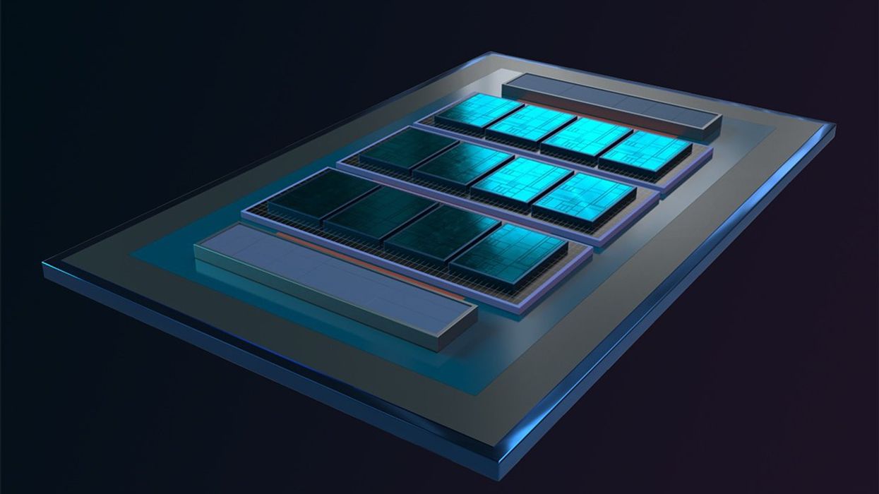
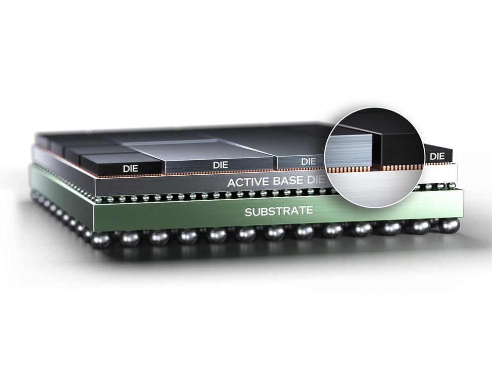
This may sound like business as usual for a foundry, but Intel for years waffled over its commitment to a foundry model. In fact, it was viewed as an IDM that only began selling wafers to customers as the cost of maintaining its own fab began to skyrocket out of country. Creating separation between the two is a fundamental shift, and it’s an essential one for building trust in a complex world of sometimes partners, sometimes competitors. In the past, the company closely guarded its IP, confining that to its own processors rather than unbundling it and selling it to potential competitors. With this new division, Intel potentially can generate profits both from customized chips that leverage technologies it develops internally for other applications, as well as its own chip business.

Gelsinger is adamant about this being a leading-edge technology company, not a supplier of all components required in systems. “I’m not going to solve 200mm supply chain issues,” he said. “And, by the way, there are not going to be more 200mm factories built, for the most part, outside of specialty like SiC. There are some crazy discussions, like when some Europeans say, ‘I don’t need a leading-edge factory in Europe. Give me a 40nm node.’ What a stupid statement. It takes 5 years to build a new 40nm node, which is already 20 years old, and to make it economically viable, we’re going to have to run it 30 more years. Move the designs to more modern nodes as opposed to expecting to build old factories that are already out of date.”

Put in perspective, Intel is basically taking the Apple approach to chipmaking. How it fares against the other two leading-edge foundries isn’t clear at this point. Until 22nm, which was 16/14nm for Samsung and TSMC, Intel was the front runner in process technology. Several nodes later, it was trailing both Samsung and TSMC. The company is on a mission to regain its leadership.

“Great industries have two or three strong players,” said Gelsinger. “TSMC is a great company, and we’re going to build a great foundry, as well. And we’re going to challenge each other to further greatness. They are the best company in terms of customer support, bar none, in the industry, and they do not have a legacy of leadership technologies. They implement technologies with great customer support. We have a deep legacy of leadership technologies across domains that we created…At our innovation conference in September, I showed three companies participating in chiplet standardization — Synopsys, Intel, and TSMC. With our test chips — with our test chips. The world wants chiplets across a range of suppliers. I think we’ll be doing some of that. I think they’re going to be doing some of that. And I want to make sure that our mutual customers have great choice and technology benefits.”

If successful, Intel Foundry may not be the lowest-cost chipmaker, as TSMC founder Morris Chang has intimated. But if it can win back some key customers, and attract a lot of new ones with better performance, higher energy efficiency, and more customization options, that may not matter. What does matter is execution on the roadmap, and the number of companies rallying around Intel appears to indicate that significant changes are afoot, and that the competitive landscape could be a lot more fluid than it was several years ago.

The post Intel, And Others, Inside appeared first on Semiconductor Engineering.

A Peek at Intel’s Future Foundry Tech


In an exclusive interview ahead of an invite-only event today in San Jose, Intel outlined new chip technologies it will offer its foundry customers by sharing a glimpse into its future data-center processors. The advances include more dense logic and a 16-fold increase in the connectivity within 3D-stacked chips, and they will be among the first top-end technologies the company has ever shared with chip architects from other companies.

The new technologies will arrive at the culmination of a years-long transformation for Intel. The processor maker is moving from being a company that produces only its own chips to becoming a foundry, making chips for others and considering its own product teams as just another customer. The San Jose event, IFS Direct Connect, is meant as a sort of coming-out party for the new business model.

Internally, Intel plans to use the combination of technologies in a server CPU code-named Clearwater Forest. The company considers the product, a system-on-a-chip with hundreds of billions of transistors, an example of what other customers of its foundry business will be able to achieve.

“Our objective is to get the compute to the best performance per watt we can achieve” from Clearwater Forest, said Eric Fetzer, director of data center technology and pathfinding at Intel. That means using the company’s most advanced fabrication technology available, Intel 18A.

3D stacking “improves the latency between compute and memory by shortening the hops, while at the same time enabling a larger cache” —Pushkar Ranade

“However, if we apply that technology throughout the entire system, you run into other potential problems,” he added. “Certain parts of the system don’t necessarily scale as well as others. Logic typically scales generation to generation very well with Moore’s Law.” But other features do not. SRAM, a CPU’s cache memory, has been lagging logic, for example. And the I/O circuits that connect a processor to the rest of a computer are even further behind.

Faced with these realities, as all makers of leading-edge processors are now, Intel broke Clearwater Forest’s system down into its core functions, chose the best-fit technology to build each, and stitched them back together using a suite of new technical tricks. The result is a CPU architecture capable of scaling to as many as 300 billion transistors.

In Clearwater Forest, billions of transistors are divided among three different types of silicon ICs, called dies or chiplets, interconnected and packaged together. The heart of the system is as many as 12 processor-core chiplets built using the Intel 18A process. These chiplets are 3D-stacked atop three “base dies” built using Intel 3, the process that makes compute cores for the Sierra Forest CPU, due out this year. Housed on the base die will be the CPU’s main cache memory, voltage regulators, and internal network. “The stacking improves the latency between compute and memory by shortening the hops, while at the same time enabling a larger cache,” says senior principal engineer Pushkar Ranade.

Finally, the CPU’s I/O system will be on two dies built using Intel 7, which in 2025 will be trailing the company’s most advanced process by a full four generations. In fact, the chiplets are basically the same as those going into the Sierra Forest and Granite Rapids CPUs, lessening the development expense.

Here’s a look at the new technologies involved and what they offer:

3D Hybrid Bonding

3D rendering of stacks of slabs with silver balls between them. The balls are larger at the bottom and smaller at the top. 3D hybrid bonding links compute dies to base dies.Intel

Intel’s current chip-stacking interconnect technology, Foveros, links one die to another using a vastly scaled-down version of how dies have long been connected to their packages: tiny “microbumps” of solder that are briefly melted to join the chips. This lets today’s version of Foveros, which is used in the Meteor Lake CPU, make one connection roughly every 36 micrometers. Clearwater Forest will use new technology, Foveros Direct 3D, which departs from solder-based methods to bring a whopping 16-fold increase in the density of 3D connections.

Called “hybrid bonding,” it’s analogous to welding together the copper pads at the face of two chips. These pads are slightly recessed and surround by insulator. The insulator on one chip affixes to the other when they are pressed together. Then the stacked chips are heated, causing the copper to expand across the gap and bind together to form a permanent link. Competitor TSMC uses a version of hybrid bonding in certain AMD CPUs to connect extra cache memory to processor-core chiplets and, in AMD’s newest GPU, to link compute chiplets to the system’s base die.

“The hybrid bond interconnects enable a substantial increase in density” of connections, says Fetzer. “That density is very important for the server market, particularly because the density drives a very low picojoule-per-bit communication.” The energy involved in data crossing from one silicon die to another can easily consume a big chunk of a product’s power budget if the per-bit energy cost is too high. Foveros Direct 3D brings that cost down below 0.05 picojoules per bit, which puts it on the same scale as the energy needed to move bits around within a silicon die.

A lot of that energy savings comes from the data traversing less copper. Say you wanted to connect a 512-wire bus on one die to the same-size bus on another so the two dies can share a coherent set of information. On each chip, these buses might be as narrow as 10–20 wires per micrometer. To get that from one die to the other using today’s 36-micrometer-pitch microbump tech would mean scattering those signals across several hundred square micrometers of silicon on one side and then gathering them across the same area on the other. Charging up all that extra copper and solder “quickly becomes both a latency and a large power problem,” says Fetzer. Hybrid bonding, in contrast, could do the bus-to-bus connection in the same area that a few microbumps would occupy.

As great as those benefits might be, making the switch to hybrid bonding isn’t easy. To forge hybrid bonds requires linking an already-diced silicon die to one that’s still attached to its wafer. Aligning all the connections properly means the chip must be diced to much greater tolerances than is needed for microbump technologies. Repair and recovery, too, require different technologies. Even the predominant way connections fail is different, says Fetzer. With microbumps, you are more likely to get a short from one bit of solder connecting to a neighbor. But with hybrid bonding, the danger is defects that lead to open connections.

Backside power

One of the main distinctions the company is bringing to chipmaking this year with its Intel 20A process, the one that will precede Intel 18A, is backside power delivery. In processors today, all interconnects, whether they’re carrying power or data, are constructed on the “front side” of the chip, above the silicon substrate. Foveros and other 3D-chip-stacking tech require through-silicon vias, interconnects that drill down through the silicon to make connections from the other side. But back-side power delivery goes much further. It puts all of the power interconnects beneath the silicon, essentially sandwiching the layer containing the transistors between two sets of interconnects.

A dark grey tower with jagged copper portions snaking up it. PowerVia puts the silicon’s power supply network below, leaving more room for data-carrying interconnects above.Intel
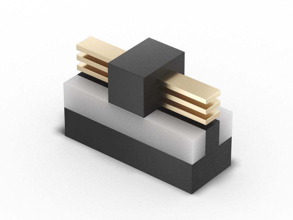
This arrangement makes a difference because power interconnects and data interconnects require different features. Power interconnects need to be wide to reduce resistance, while data interconnects should be narrow so they can be densely packed. Intel is set to be the first chipmaker to introduce back-side power delivery in a commercial chip, later this year with the release of the Arrow Lake CPU. Data released last summer by Intel showed that back-side power alone delivered a 6 percent performance boost.

The Intel 18A process technology’s back-side-power-delivery network technology will be fundamentally the same as what’s found in Intel 20A chips. However, it’s being used to greater advantage in Clearwater Forest. The upcoming CPU includes what’s called an “on-die voltage regulator” within the base die. Having the voltage regulation close to the logic it drives means the logic can run faster. The shorter distances let the regulator respond to changes in the demand for current more quickly, while consuming less power.

Because the logic dies use back-side power delivery, the resistance of the connection between the voltage regulator and the dies logic is that much lower. “The power via technology along with the Foveros stacking gives us a really efficient way to hook it up,” says Fetzer.

RibbonFET, the next generation

In addition to back-side power, the chipmaker is switching to a different transistor architecture with the Intel 20A process: RibbonFET. A form of nanosheet, or gate-all-around, transistor, RibbonFET replaces the FinFET, CMOS’s workhorse transistor since 2011. With Intel 18A, Clearwater Forest’s logic dies will be made with a second generation of RibbonFET process. While the devices themselves aren’t very different from the ones that will emerge from Intel 20A, there’s more flexibility to the design of the devices, says Fetzer.

Three gold ribbons pass through a dark grey block. RibbonFET is Intel’s take on nanowire transistors.Intel
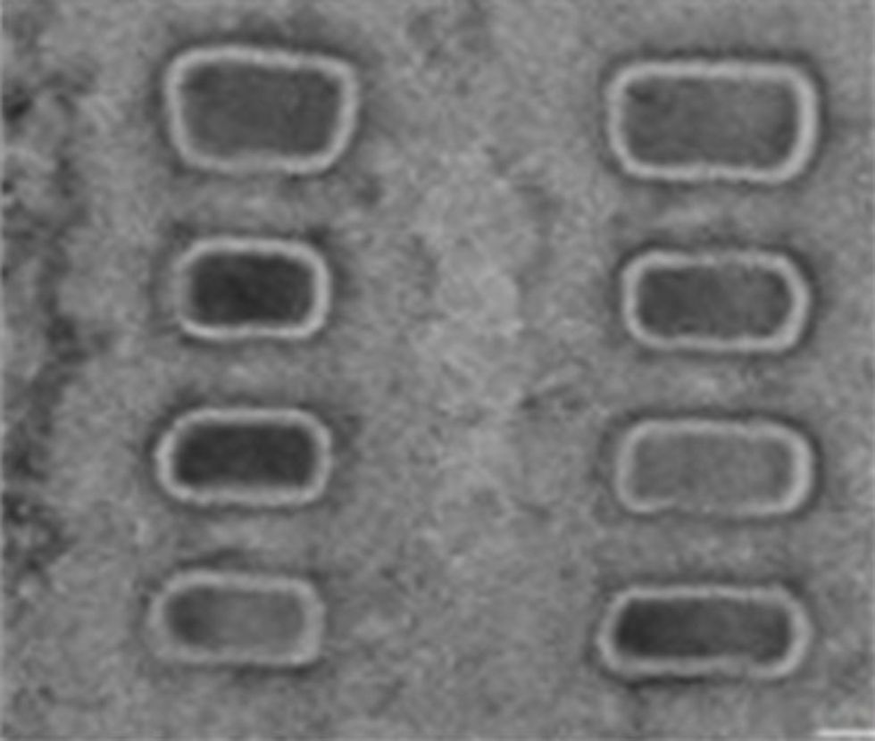
“There’s a broader array of devices to support various foundry applications beyond just what was needed to enable a high-performance CPU,” which was what the Intel 20A process was designed for, he says.

Two vertical towers of dark grey blocks embedded in grainy light grey material. RibbonFET’s nanowires can have different widths depending on the needs of a logic cell.Intel
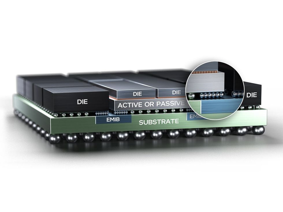
Some of that variation stems from a degree of flexibility that was lost in the FinFET era. Before FinFETs arrived, transistors in the same process could be made in a range of widths, allowing a more-or-less continuous trade-off between performance—which came with higher current—and efficiency—which required better control over leakage current. Because the main part of a FinFET is a vertical silicon fin of a defined height and width, that trade-off now had to take the form of how many fins a device had. So, with two fins you could double current, but there was no way to increase it by 25 or 50 percent.

With nanosheet devices, the ability to vary transistor widths is back. “RibbonFET technology enables different sizes of ribbon within the same technology base,” says Fetzer. “When we go from Intel 20A to Intel 18A, we offer more flexibility in transistor sizing.”

That flexibility means that standard cells, basic logic blocks designers can use to build their systems, can contain transistors with different properties. And that enabled Intel to develop an “enhanced library” that includes standard cells that are smaller, better performing, or more efficient than those of the Intel 20A process.

2nd generation EMIB

In Clearwater Forest, the dies that handle input and output connect horizontally to the base dies—the ones with the cache memory and network—using the second generation of Intel’s EMIB. EMIB is a small piece of silicon containing a dense set of interconnects and microbumps designed to connect one die to another in the same plane. The silicon is embedded in the package itself to form a bridge between dies.

3D rendering of stacks of slabs with silver balls between them. The balls are larger at the bottom and smaller at the top. Dense 2D connections are formed by a small sliver of silicon called EMIB, which is embedded in the package substrate.Intel

The technology has been in commercial use in Intel CPUs since Sapphire Rapids was released in 2023. It’s meant as a less costly alternative to putting all the dies on a silicon interposer, a slice of silicon patterned with interconnects that is large enough for all of the system’s dies to sit on. Apart from the cost of the material, silicon interposers can be expensive to build, because they are usually several times larger than what standard silicon processes are designed to make.

The second generation of EMIB debuts this year with the Granite Rapids CPU, and it involves shrinking the pitch of microbump connections from 55 micrometers to 45 micrometers as well as boosting the density of the wires. The main challenge with such connections is that the package and the silicon expand at different rates when they heat up. This phenomenon could lead to warpage that breaks connections.

What’s more, in the case of Clearwater Forest “there were also some unique challenges, because we’re connecting EMIB on a regular die to EMIB on a Foveros Direct 3D base die and a stack,” says Fetzer. This situation, recently rechristened EMIB 3.5 technology (formerly called co-EMIB), requires special steps to ensure that the stresses and strains involved are compatible with the silicon in the Foveros stack, which is thinner than ordinary chips, he says.

For more, see Intel’s whitepaper on their foundry tech.

❌