Metrology And Inspection For The Chiplet Era
New developments and innovations in metrology and inspection will enable chipmakers to identify and address defects faster and with greater accuracy than ever before, all of which will be required at future process nodes and in densely-packed assemblies of chiplets.
These advances will affect both front-end and back-end processes, providing increased precision and efficiency, combined with artificial intelligence/machine learning and big data analytics. These kinds of improvements will be crucial for meeting the industry’s changing needs, enabling deeper insights and more accurate measurements at rates suitable for high-volume manufacturing. But gaps still need to be filled, and new ones are likely to show up as new nodes and processes are rolled out.
“As semiconductor devices become more complex, the demand for high-resolution, high-accuracy metrology tools increases,” says Brad Perkins, product line manager at Nordson Test & Inspection. “We need new tools and techniques that can keep up with shrinking geometries and more intricate designs.”
The shift to high-NA EUV lithography (0.55 NA EUV) at the 2nm node and beyond is expected to exacerbate stochastic variability, demanding more robust metrology solutions on the front end. Traditional critical dimension (CD) measurements alone are insufficient for the level of analysis required. Comprehensive metrics, including line-edge roughness (LER), line-width roughness (LWR), local edge-placement error (LEPE), and local CD uniformity (LCDU), alongside CD measurements, are necessary for ensuring the integrity and performance of advanced semiconductor devices. These metrics require sophisticated tools that can capture and analyze tiny variations at the nanometer scale, where even slight discrepancies can significantly impact device functionality and yield.
“Metrology is now at the forefront of yield, especially considering the current demands for DRAM and HBM,” says Hamed Sadeghian, president and CEO of Nearfield Instruments. “The next generations of HBMs are approaching a stage where hybrid bonding will be essential due to the increasing stack thickness. Hybrid bonding requires high resolutions in vertical directions to ensure all pads, and the surface height versus the dielectric, remain within nanometer-scale process windows. Consequently, the tools used must be one order of magnitude more precise.”
To address these challenges, companies are developing hybrid metrology systems that combine various measurement techniques for a comprehensive data set. Integrating scatterometry, electron microscopy, and/or atomic force microscopy allows for more thorough analysis of critical features. Moreover, AI and ML algorithms enhance the predictive capabilities of these tools, enabling process adjustments.
“Our customers who are pushing into more advanced technology nodes are desperate to understand what’s driving their yield,” says Ronald Chaffee, senior director of applications engineering at NI/Emerson Test & Measurement. “They may not know what all the issues are, but they are gathering all possible data — metrology, AEOI, and any measurable parameters — and seeking correlations.”
Traditional methods for defect detection, pattern recognition, and quality control typically used spatial pattern-recognition modules and wafer image-based algorithms to address wafer-level issues. “However, we need to advance beyond these techniques,” says Prasad Bachiraju, senior director of business development at Onto Innovation. “Our observations show that about 20% of wafers have systematic issues that can limit yield, with nearly 4% being new additions. There is a pressing need for advanced metrology for in-line monitoring to achieve zero-defect manufacturing.”
Several companies recently announced metrology innovations to provide more precise inspections, particularly for difficult-to-see areas, edge effects, and highly reflective surfaces.
Nordson unveiled its AMI SpinSAM acoustic rotary scan system. The system represents a significant departure from traditional raster scan methods, utilizing a rotational scanning approach. Rather than moving the wafer in an x,y pattern relative to a stationary lens, the wafer spins, similar to a record player. This reduces motion over the wafer and increases inspection speed, negating the need for image stitching and improving image quality.
“For years, we’d been trying to figure out this technique, and it’s gratifying to finally achieve it. It’s something we’ve always thought would be incredibly beneficial,” says Perkins. “The SpinSAM is designed primarily to enhance inspection speed and efficiency, addressing the common industry demand for more product throughput and better edge inspection capabilities.”
Meanwhile, Nearfield Instruments introduced a multi-head atomic force microscopy (AFM) system called QUADRA. It is a high-throughput, non-destructive metrology tool for HVM that features a novel multi-miniaturized AFM head architecture. Nearfield claims the parallel independent multi-head scanner can deliver a 100-fold throughput advantage versus conventional single-probe AFM tools. This architecture allows for precise measurements of high-aspect-ratio structures and complex 3D features, critical for advanced memory (3D NAND, DRAM, HBM) and logic processes.

Fig. 1: Image capture comparison of standard AFM and multi-head AFM. Source: Nearfield Instruments
In April, Onto Innovation debuted an advancement in subsurface defect inspection technology with the release of its Dragonfly G3 inspection system. The new system allows for 100% wafer inspection, targeting subsurface defects that can cause yield losses, such as micro-cracks and other hidden flaws that may lead to entire wafers breaking during subsequent processing steps. The Dragonfly G3 utilizes novel infrared (IR) technology combined with specially designed algorithms to detect these defects, which previously were undetectable in a production environment. This new capability supports HBM, advanced logic, and various specialty segments, and aims to improve final yield and cost savings by reducing scrapped wafers and die stacks.
More recently, researchers at the Paul Scherrer Institute announced a high-performance X-ray tomography technique using burst ptychography. This new method can provide non-destructive, detailed views of nanostructures as small as 4nm in materials like silicon and metals at a fast acquisition rate of 14,000 resolution elements per seconds. The tomographic back-propagation reconstruction allows imaging of samples up to ten times larger than the conventional depth of field.
There are other technologies and techniques for improving metrology in semiconductor manufacturing, as well, including wafer-level ultrasonic inspection, which involves flipping the wafer to inspect from the other side. New acoustic microscopy techniques, such as scanning acoustic microscopy (SAM) and time-of-flight acoustic microscopy (TOF-AM), enable the detection and characterization of very small defects, such as voids, delaminations, and cracks within thin films and interfaces.
“We used to look at 80 to 100 micron resist films, but with 3D integrated packaging, we’re now dealing with films that are 160 to 240 microns—very thick resist films,” says Christopher Claypool, senior application scientist at Bruker OCD. “In TSVs and microbumps, the dominant technique today is white light interferometry, which provides profile information. While it has some advantages, its throughput is slow, and it’s a focus-based technique. This limitation makes it difficult to measure TSV structures smaller than four or five microns in diameter.”
Acoustic metrology tools equipped with the newest generation of focal length transducers (FLTs) can focus acoustic waves with precision down to a few nanometers, allowing for non-destructive detailed inspection of edge defects and critical stress points. This capability is particularly useful for identifying small-scale defects that might be missed by other inspection methods.
The development and integration of smart sensors in metrology equipment is instrumental in collecting the vast amounts of data needed for precise measurement and quality control. These sensors are highly sensitive and capable of operating under various environmental conditions, ensuring consistent performance. One significant advantage of smart sensors is their ability to facilitate predictive maintenance. By continuously monitoring the health and performance of metrology equipment, these sensors can predict potential failures and schedule maintenance before significant downtime occurs. This capability enhances the reliability of the equipment, reduces maintenance costs, and improves overall operational efficiency.
Smart sensors also are being developed to integrate seamlessly with metrology systems, offering real-time data collection and analysis. These sensors can monitor various parameters throughout the manufacturing process, providing continuous feedback and enabling quick adjustments to prevent defects. Smart sensors, combined with big data platforms and advanced data analytics, allow for more efficient and accurate defect detection and classification.
Critical stress points
A persistent challenge in semiconductor metrology is the identification and inspection of defects at critical stress points, particularly at the silicon edges. For bonded wafers, it’s at the outer ring of the wafer. For chip-on-wafer packaging, it’s at the edge of the chips. These edge defects are particularly problematic because they occur at the highest stress points from the neutral axis, making them more prone to failures. As semiconductor devices continue to involve more intricate packaging techniques, such as chip-on-wafer and wafer-level packaging, the focus on edge inspection becomes even more critical.
“When defects happen in a factory, you need imaging that can detect and classify them,” says Onto’s Bachiraju. “Then you need to find the root causes of where they’re coming from, and for that you need the entire data integration and a big data platform to help with faster analysis.”
Another significant challenge in semiconductor metrology is ensuring the reliability of known good die (KGD), especially as advanced packaging techniques and chiplets become more prevalent. Ensuring that every chip/chiplet in a stacked die configuration is of high quality is essential for maintaining yield and performance, but the speed of metrology processes is a constant concern. This leads to a balancing act between thoroughness and efficiency. The industry continuously seeks to develop faster machines that can handle the increasing volume and complexity of inspections without compromising accuracy. In this race, innovations in data processing and analysis are key to achieving quicker results.
“Customers would like, generally, 100% inspection for a lot of those processes because of the known good die, but it’s cost-prohibitive because the machines just can’t run fast enough,” says Nordson’s Perkins.
Metrology and Industry 4.0
Industry 4.0 — a term introduced in Germany in 2011 for the fourth industrial revolution, and called smart manufacturing in the U.S. — emphasizes the integration of digital technologies such as the Internet of Things, artificial intelligence, and big data analytics into manufacturing processes. Unlike past revolutions driven by mechanization, electrification, and computerization, Industry 4.0 focuses on connectivity, data, and automation to enhance manufacturing capabilities and efficiency.
“The better the data integration is, the more efficient the yield ramp,” says Dieter Rathei, CEO of DR Yield. “It’s essential to integrate all available data into the system for effective monitoring and analysis.”
In semiconductor manufacturing, this shift toward Industry 4.0 is particularly transformative, driven by the increasing complexity of semiconductor devices and the demand for higher precision and yield. Traditional metrology methods, heavily reliant on manual processes and limited automation, are evolving into highly interconnected systems that enable real-time data sharing and decision-making across the entire production chain.
“There haven’t been many tools to consolidate different data types into a single platform,” says NI’s Chaffee. “Historically, yield management systems focused on testing, while FDC or process systems concentrated on the process itself, without correlating the two. As manufacturers push into the 5, 3, and 2nm spaces, they’re discovering that defect density alone isn’t the sole governing factor. Process control is also crucial. By integrating all data, even the most complex correlations that a human might miss can be identified by AI and ML. The goal is to use machine learning to detect patterns or connections that could help control and optimize the manufacturing process.”
IoT forms the backbone of Industry 4.0 by connecting various devices, sensors, and systems within the manufacturing environment. In semiconductor manufacturing, IoT enables seamless communication between metrology tools, production equipment, and factory management systems. This interconnected network facilitates real-time monitoring and control of manufacturing processes, allowing for immediate adjustments and optimization.
“You need to integrate information from various sources, including sensors, metrology tools, and test structures, to build predictive models that enhance process control and yield improvement,” says Michael Yu, vice president of advanced solutions at PDF Solutions. “This holistic approach allows you to identify patterns and correlations that were previously undetectable.”
AI and ML are pivotal in processing and analyzing the vast amounts of data generated in a smart factory. These technologies can identify patterns, predict equipment failures, and optimize process parameters with a level of precision and speed unattainable by human operators alone. In semiconductor manufacturing, AI-driven analytics enhance process control, improve yield rates, and reduce downtime. “One of the major trends we see is the integration of artificial intelligence and machine learning into metrology tools,” says Perkins. “This helps in making sense of the vast amounts of data generated and enables more accurate and efficient measurements.”
AI’s role extends further as it assists in discovering anomalies within the production process that might have gone unnoticed with traditional methods. AI algorithms integrated into metrology systems can dynamically adjust processes in real-time, ensuring that deviations are corrected before they affect the end yield. This incorporation of AI minimizes defect rates and enhances overall production quality.
“Our experience has shown that in the past 20 years, machine learning and AI algorithms have been critical for automatic data classification and die classification,” says Bachiraju. “This has significantly improved the efficiency and accuracy of our metrology tools.”
Big data analytics complements AI/ML by providing the infrastructure necessary to handle and interpret massive datasets. In semiconductor manufacturing, big data analytics enables the extraction of actionable insights from data generated by IoT devices and production systems. This capability is crucial for predictive maintenance, quality control, and continuous process improvement.
“With big data, we can identify patterns and correlations that were previously impossible to detect, leading to better process control and yield improvement,” says Perkins.
Big data analytics also helps in understanding the lifecycle of semiconductor devices from production to field deployment. By analyzing product performance data over time, manufacturers can predict potential failures and enhance product designs, increasing reliability and lifecycle management.
“In the next decade, we see a lot of opportunities for AI,” says DR Yield’s Rathei. “The foundation for these advancements is the availability of comprehensive data. AI models need extensive data for training. Once all the data is available, we can experiment with different models and ideas. The ingenuity of engineers, combined with new tools, will drive exponential progress in this field.”
Metrology gaps remain
Despite recent advancements in metrology, analytics, and AI/ML, several gaps still remain, particularly in the context of high-volume manufacturing (HVM) and next-generation devices. The U.S. Commerce Department’s CHIPS R&D Metrology Program, along with industry stakeholders, have highlighted seven “grand challenges,” areas where current metrology capabilities fall short:
Metrology for materials purity and properties: There is a critical need for new measurements and standards to ensure the purity and physical properties of materials used in semiconductor manufacturing. Current techniques lack the sensitivity and throughput required to detect particles and contaminants throughout the supply chain.
Advanced metrology for future manufacturing: Next-generation semiconductor devices, such as gate-all-around (GAA) FETs and complementary FETs (CFETs), require breakthroughs in both physical and computational metrology. Existing tools are not yet capable of providing the resolution, sensitivity, and accuracy needed to characterize the intricate features and complex structures of these devices. This includes non-destructive techniques for characterizing defects and impurities at the nanoscale.
“There is a secondary challenge with some of the equipment in metrology, which often involves sampling data from single points on a wafer, much like heat test data that only covers specific sites,” says Chaffee. “To be meaningful, we need to move beyond sampling methods and find creative ways to gather information from every wafer, integrating it into a model. This involves building a knowledge base that can help in detecting patterns and correlations, which humans alone might miss. The key is to leverage AI and machine learning to identify these correlations and make sense of them, especially as we push into the 5, 3, and 2nm spaces. This process is iterative and requires a holistic approach, encompassing various data points and correlating them to understand the physical boundaries and the impact on the final product.”
Metrology for advanced packaging: The integration of sophisticated components and novel materials in advanced packaging technologies presents significant metrology challenges. There is a need for rapid, in-situ measurements to verify interfaces, subsurface interconnects, and internal 3D structures. Current methods do not adequately address issues such as warpage, voids, substrate yield, and adhesion, which are critical for the reliability and performance of advanced packages.
Modeling and simulating semiconductor materials, designs, and components: Modeling and simulating semiconductor processes require advanced computational models and data analysis tools. Current capabilities are limited in their ability to seamlessly integrate the entire semiconductor value chain, from materials inputs to system assembly. There is a need for standards and validation tools to support digital twins and other advanced simulation techniques that can optimize process development and control.
“Predictive analytics is particularly important,” says Chaffee. “They aim to determine the probability of any given die on a wafer being the best yielding or presenting issues. By integrating various data points and running different scenarios, they can identify and understand how specific equipment combinations, sequences and processes enhance yields.”
Modeling and simulating semiconductor processes: Current capabilities are limited in their ability to seamlessly integrate the entire semiconductor value chain, from materials inputs to system assembly. There is a need for standards and validation tools to support digital twins and other advanced simulation techniques that can optimize process development and control.
“Part of the problem comes from the back-end packaging and assembly process, but another part of the problem can originate from the quality of the wafer itself, which is determined during the front-end process,” says PDF’s Yu. “An effective ML model needs to incorporate both front-end and back-end information, including data from equipment sensors, metrology, and structured test information, to make accurate predictions and take proactive actions to correct the process.”
Standardizing new materials and processes: The development of future information and communication technologies hinges on the creation of new standards and validation methods. Current reference materials and calibration services do not meet the requirements for next-generation materials and processes, such as those used in advanced packaging and heterogeneous integration. This gap hampers the industry’s ability to innovate and maintain competitive production capabilities.
Metrology to enhance security and provenance of components and products: With the increasing complexity of the semiconductor supply chain, there is a need for metrology solutions that can ensure the security and provenance of components and products. This involves developing methods to trace materials and processes throughout the manufacturing lifecycle to prevent counterfeiting and ensure compliance with regulatory standards.
“The focus on security and sharing changes the supplier relationship into more of a partnership and less of a confrontation,” says Chaffee. “Historically, there’s always been a concern of data flowing across that boundary. People are very protective about their process, and other people are very protective about their product. But once you start pushing into the deep sub-micron space, those barriers have to come down. The die are too expensive for them not to communicate, but they can still do so while protecting their IP. Companies are starting to realize that by sharing parametric test information securely, they can achieve better yield management and process optimization without compromising their intellectual property.”
Conclusion
Advancements in metrology and testing are pivotal for the semiconductor industry’s continued growth and innovation. The integration of AI/ML, IoT, and big data analytics is transforming how manufacturers approach process control and yield improvement. As adoption of Industry 4.0 grows, the role of metrology will become even more critical in ensuring the efficiency, quality, and reliability of semiconductor devices. And by leveraging these advanced technologies, semiconductor manufacturers can achieve higher yields, reduce costs, and maintain the precision required in this competitive industry.
With continuous improvements and the integration of smart technologies, the semiconductor industry will keep pushing the boundaries of innovation, leading to more robust and capable electronic devices that define the future of technology. The journey toward a fully realized Industry 4.0 is ongoing, and its impact on semiconductor manufacturing undoubtedly will shape the future of the industry, ensuring it stays at the forefront of global technological advancements.
“Anytime you have new packaging technologies and process technologies that are evolving, you have a need for metrology,” says Perkins. “When you are ramping up new processes and need to make continuous improvements for yield, that is when you see the biggest need for new metrology solutions.”
The post Metrology And Inspection For The Chiplet Era appeared first on Semiconductor Engineering.


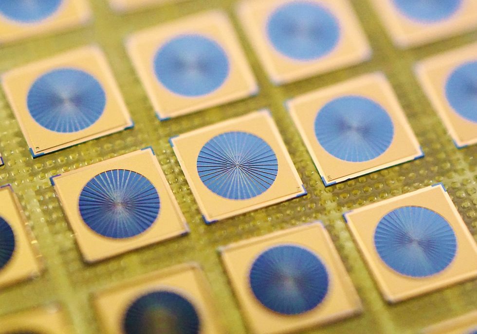 Multiple 3-millimeter-wide photonic-crystal semiconductor lasers are built on a semiconductor wafer. Susumu Noda
