FreshRSS

Zobrazení pro čtení

Jsou dostupné nové články, klikněte pro obnovení stránky.

AMD Launches New Ryzen & Radeon Gaming Bundle: Warhammer 40,000: Space Marine 2 and Unknown 9: Awakening

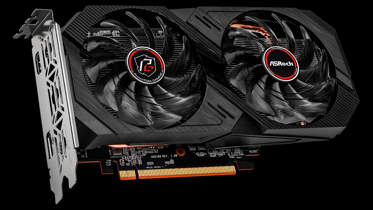
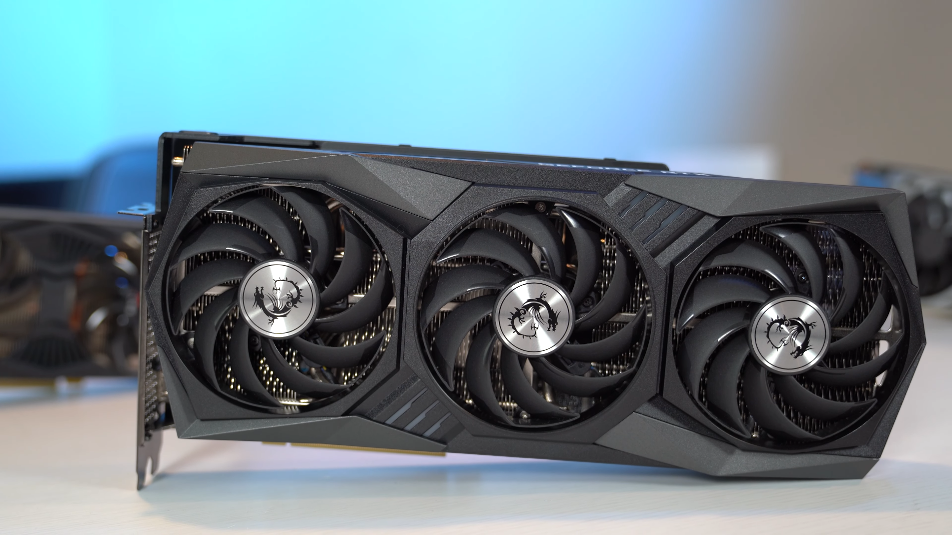
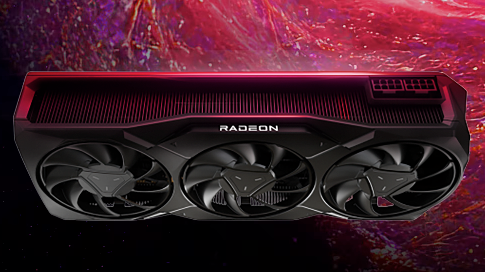
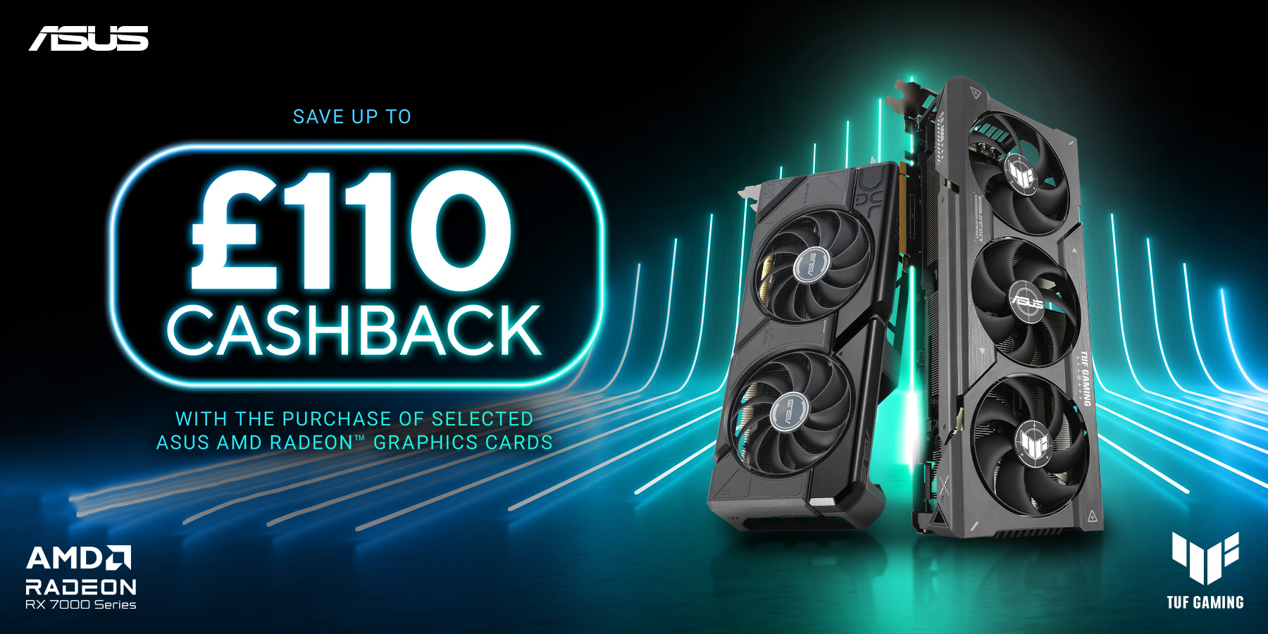
AMD has made itself quite a reputation with its bundling campaigns over the years, and every new season we can be sure that the company will be giving away free games with the purchase of its hardware. This summer will certainly not be exception as AMD will be bundling Warhammer 40,000: Space Marine 2 and Unknown 9: Awakening titles with its Ryzen 7000 CPUs and Radeon RX 7000 video cards.

The latest bundle offer essentially covers all of AMD's existing mid-range and high-end consumer desktop products, sans the to-be-launched Ryzen 9000 series. That includes not only AMD's desktop parts, such as the Ryzen 9 7800X3D, but also virtually their entire stack of Radeon RX 7000 video cards, right on down to the 7600 XT.

AMD's laptop hardware is also covered as well, which is a much rarer occurence. Mid-range and high-end Ryzen 7000 mobile parts are part of the game bundle, including the 7940HS and even the 7435HS. However the refreshed version of these parts, sold under the Ryzen 8000 Mobile line, are not. Meanwhile systems with a Radeon RX 7700S or 7600S mobile GPU are included as well.

This deal is available only through participating retailers (in case of the U.S. and Canada these are Amazon and Newegg). The promotion is also applicable to select laptops containing these components. 

AMD's Summer 2024 Ryzen & Radeon Game Bundle
(Warhammer 40,000: Space Marine 2 & Unknown 9: Awakening)
  CPU GPU
Desktop Ryzen 9 7950X3D
Ryzen 9 7950X
Ryzen 9 7900X3D
Ryzen 9 7900X
Ryzen 9 7900*
Ryzen 7 7800X3D*
Ryzen 7 7700X*
Ryzen 7 7700*
Radeon RX 7900 XTX
Radeon RX 7900 XT
Radeon RX 7900 GRE
Radeon RX 7800 XT*
Radeon RX 7700 XT*
Radeon RX 7600 XT*
Laptop Ryzen 9 7940HS
Ryzen 7 7840HS
Ryzen 7 7735HS
Ryzen 7 7435HS
Radeon RX 7700S
Radeon RX 7600S
*This product does not qualify for the promotion in Japan

Warhammer 40,000: Space Marine 2 carries an MSRP of $60, whereas the Unknown 9: Awakening is set at $50, so this offer provides an estimated value of $110. The deal is particularly appealing to gamers and those interested in action titles. Meanwhile, fans of such games probably already have AMD's Ryzen 7000 and Radeon RX 7000-series products, so while the deal will be appealing to some users, it may not be appealing for gamers looking to upgrade to AMD's latest Zen 5-powered CPUs.

The campaign starts on August 6, 2024, at 9:00 AM ET and ends on October 5, 2024, at 11:59 PM ET, or when all Coupon Codes are claimed, whichever happens first. Coupon Codes must be redeemed by November 2, 2024, at 11:59 PM ET. 

ASRock Launches Passively Cooled Radeon RX 7900 XTX & XT Cards for Servers

As sales of GPU-based AI accelerators remain as strong as ever, the immense demand for these cards has led to some server builders going off the beaten path in order to get the hardware they want at a lower price. While both NVIDIA and AMD offer official card configurations for servers, the correspondingly high price of these cards makes them a significant financial outlay that some customers either can't afford, or don't want to pay.

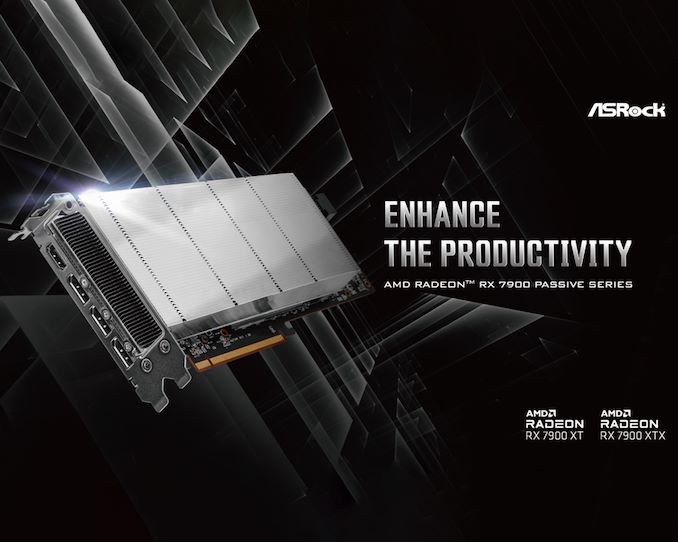
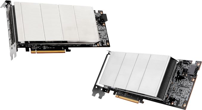
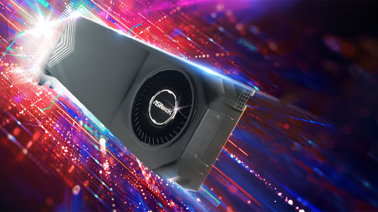
Instead, these groups have been turning to buying up consumer graphics cards, which although they come with additional limitations, are also a fraction of the cost of a "proper" server card. And this week, ASRock has removed another one of those limitations for would-be AMD Radeon users, with the introduction of a set of compact, passively-cooled Radeon RX 7900 XTX and RX 7900 XT video cards that are designed to go in servers.

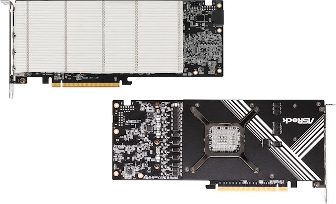
Without any doubts, ASRock's AMD Radeon RX 7900 XTX Passive 24GB and AMD Radeon RX 7900 XT Passive 20GB AIBs are indeed graphics cards with four display outputs and based on the Navi 31 graphics processor (with 6144 and 5376 stream processors, respectively), so they can output graphics and work both with games and professional applications. And with TGPs of 355W and 315W respectively, these cards aren't underclocked in any way compared to traditional desktop cards. However, unlike a typical desktop card, the cooler on these cards is a dual-slot heatsink without any kind of fan attached, which is meant to be used with high-airflow forced-air cooling.

All-told, ASRock's passive cooler is pretty capable, as well; it's not just a simple aluminum heatsink. Beneath the fins, ASRock has gone with a vapor chamber and multiple heat pipes to distribute heat to the rest of the sink. Even with forced-air cooling in racked servers, the heatsink itself still needs to be efficient to keep a 300W+ card cool with only a dual-slot cooler – and especially so when upwards of four of these cards are installed side-by-side with each other. To make the boards even more server friendly, these cards are equipped with a 12V-2×6 power connector, a first for the Radeon RX 7900 series, simplifying installation by reducing cable clutter.

Driving the demand for these cards in particular is their memory configuration. With 24GB for the 7900 XTX and 20GB for the 7900 XT is half as much (or less) memory than can be found on AMD and NVIDIA's high-end professional and server cards, AMD is the only vendor offering consumer cards with this much memory for less than $1000. So for a memory-intensive AI inference cluster built on a low budget, the cheapest 24GB card available starts looking like a tantalizing option.

Otherwise, ASRock's Radeon RX 7900 Passive cards distinguish themselves from AMD's formal professional and server cards by what they're not capable of doing: namely, remote professional graphics or other applications that need things like GPU partitioning. These parts look to be aimed at one application only, artificial intelligence, and are meant to process huge amounts of data. For this purpose, their passive coolers will do the job and the lack of ProViz or VDI-oriented drives ensure that AMD will leave these lucrative markets for itself.

NVIDIA Closes Above $135, Becomes World’s Most Valuable Company

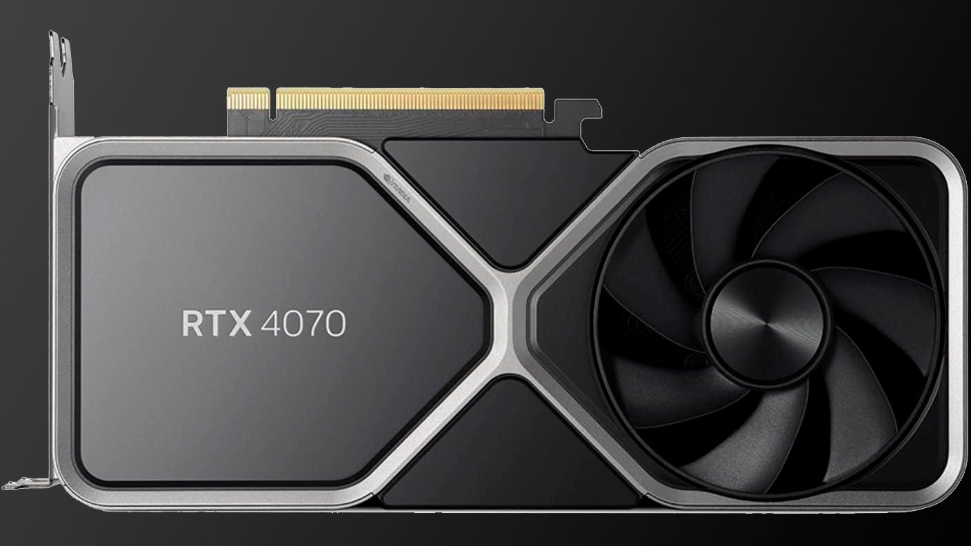
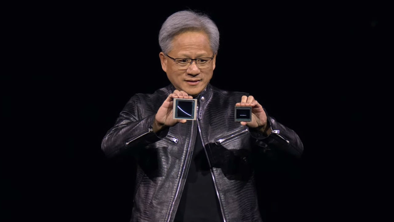
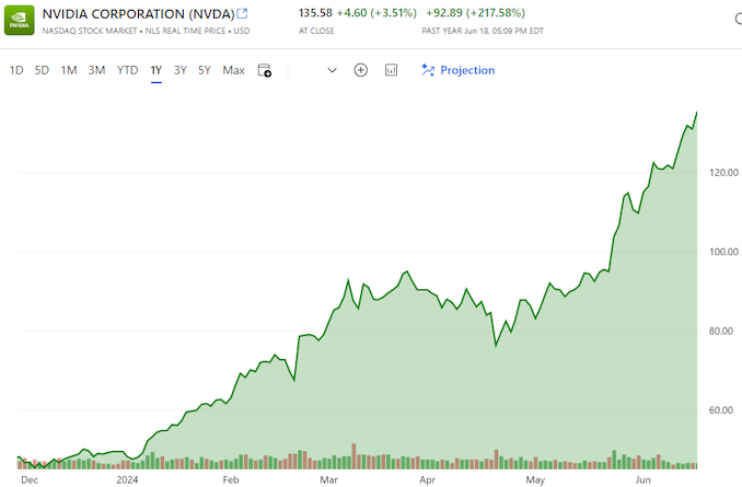
Thanks to the success of the burgeoning market for AI accelerators, NVIDIA has been on a tear this year. And the only place that’s even more apparent than the company’s rapidly growing revenues is in the company’s stock price and market capitalization. After breaking into the top 5 most valuable companies only earlier this year, NVIDIA has reached the apex of Wall Street, closing out today as the world’s most valuable company.

With a closing price of $135.58 on a day that saw NVIDIA’s stock pop up another 3.5%, NVIDIA has topped both Microsoft and Apple in valuation, reaching a market capitalization of $3.335 trillion. This follows a rapid rise in the company’s stock price, which has increased by 47% in the last month alone – particularly on the back of NVIDIA’s most recent estimates-beating earnings report – as well as a recent 10-for-1 stock split. And looking at the company’s performance over a longer time period, NVIDIA’s stock jumped a staggering 218% over the last year, or a mere 3,474% over the last 5 years.

NVIDIA’s ascension continues a trend over the last several years of tech companies all holding the top spots in the market capitalization rankings. Though this is the first time in quite a while that the traditional tech leaders of Apple and Microsoft have been pushed aside.

Market Capitalization Rankings
  Market Cap Stock Price
NVIDIA $3.335T $135.58
Microsoft $3.317T $446.34
Apple $3.285T $214.29
Alphabet $2.170T $176.45
Amazon $1.902T $182.81

Driving the rapid growth of NVIDIA and its market capitalization has been demand for AI accelerators from NVIDIA, particularly the company’s server-grade H100, H200, and GH200 accelerators for AI training. As the demand for these products has spiked, NVIDIA has been scaling up accordingly, repeatedly beating market expectations for how many of the accelerators they can ship – and what price they can charge. And despite all that growth, orders for NVIDIA’s high-end accelerators are still backlogged, underscoring how NVIDIA still isn’t meeting the full demands of hyperscalers and other enterprises.

Consequently, NVIDIA’s stock price and market capitalization have been on a tear on the basis of these future expectations. With a price-to-earnings (P/E) ratio of 76.7 – more than twice that of Microsoft or Apple – NVIDIA is priced more like a start-up than a 30-year-old tech company. But then it goes without saying that most 30-year-old tech companies aren’t tripling their revenue in a single year, placing NVIDIA in a rather unique situation at this time.

Like the stock market itself, market capitalizations are highly volatile. And historically speaking, it’s far from guaranteed that NVIDIA will be able to hold the top spot for long, never mind day-to-day fluctuations. NVIDIA, Apple, and Microsoft’s valuations are all within $50 billion (1.%) of each other, so for the moment at least, it’s still a tight race between all three companies. But no matter what happens from here, NVIDIA gets the exceptionally rare claim of having been the most valuable company in the world at some point.

(Carousel image courtesy MSN Money)

SK hynix: GDDR7 Mass Production To Start in Q4'2024

Update 06/13: SK hynix has sent a note to AnandTech clarifying that the company "plans to start mass production of GDDR7 in the fourth quarter of this year when the relevant market opens up." This article has been updated accordingly.

Being a major JEDEC memory standard, GDDR7 is slated to be produced by all three of the Big Three memory manufacturers. But it seems that not all three vendors will be kicking off mass production at the same time.

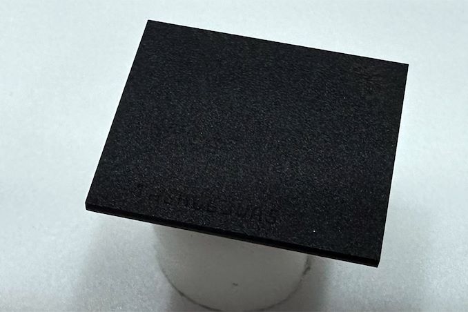
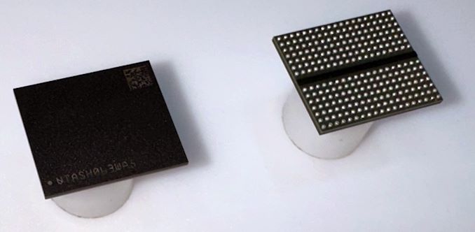
SK hynix was at this year's Computex trade show, showing off their full lineup of memory technologies – including, of course, GDDR7. SK hynix is the last of the major memory vendor's we've seen promoting their memory, and fittingly, they seem to be the last in terms of their mass production schedule. According to company representatives, the firm will kick off mass production of their GDDR7 chips in the last quarter of 2024.

Comparatively, the company's cross-town rival, Samsung, is already sampling memory with the goal of getting it out the door in 2024. And Micron has been rather gung ho about not only starting mass production this year, but starting it early enough that at least some of their customers will be able to ship finished products this year.

That said, it bears mentioning that with industry-standard memory technologies, mass production at one vendor does not indicate that another is late; it is just indicating that someone was first to validate with a partner and that partner plans to ship its product in 2024. And while mass production remains another 4+ months out, SK hynix does have sample chips for its partners to test right now, and the chips have been demonstrated at Computex.

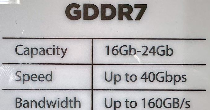
As far as SK hynix's floor booth at Computex 2024 is concerned, the company had GDDR7 chips on display along with a table essentially summarizing the company's roadmap. For now, SK hynix is planning on both 16Gbit and 24Gbit chips, with data transfer rates of up to 40 GT/s. Though when SK hynix intends to launch their higher-end configurations remains to be seen. Both of the company's rivals are starting out with 16Gbit chips running at 32 GT/sec, so being the first to get a faster/larger chip out would be a feather in SK hynix's cap.

AMD Slims Down Compute With Radeon Pro W7900 Dual Slot For AI Inference

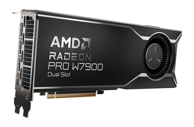
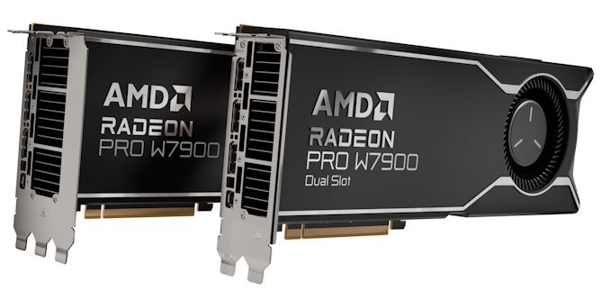
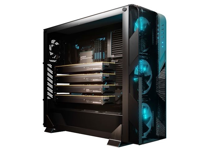
While the bulk of AMD’s Computex presentation was on CPUs and their Instinct lineup of dedicated AI accelerators, the company also has a small product refresh for the professional graphics and workstation AI crowd. AMD is releasing a dual-slot version of their high-end Radeon Pro W7900 card – aptly named the W7900 Dual Slot – with the intent being to improve compute density in workstations by making it possible to install 4 of the cards inside a single chassis.

The release of a dual-slot version of the card comes after the original Radeon Pro W7900 was the first time AMD went with a larger, triple-slot form factor for their flagship workstation card. With the W7000 generation bringing an all-around increase in power consumption, pushing the W7900 to 295 Watts, AMD originally opted to release a larger card for improved acoustics. However this came at the cost of compute density, as most systems could only fit 2 of the thicker cards. As a result, AMD is opting to release a dual-slot version of the hardware as well, to offer a more competitive product for high-density workstation systems – particularly those doing local AI inference.

AMD Radeon Pro Specification Comparison
  AMD Radeon Pro W7900DS AMD Radeon Pro W7900 AMD Radeon Pro W7800 AMD Radeon Pro W6800
ALUs 12288
(96 CUs)
8960
(70 CUs)
3840
(60 CUs)
ROPs 192 128 96
Boost Clock 2.495GHz 2.495GHz 2.32HHz
Peak Throughput (FP32) 61.3 TFLOPS 45.2 TFLOPS 17.8 TFLOPS
Memory Clock 18 Gbps GDDR6 18 Gbps GDDR6 16 Gbps GDDR6
Memory Bus Width 384-bit 256-bit 256-bit
Memiry Bandwidth 864GB/sec 576GB/sec 512GB/sec
VRAM 48GB 32GB 32GB
ECC Yes
(DRAM)
Yes
(DRAM)
Yes
(DRAM)
Infinity Cache 96MB 64MB 128MB
Total Board Power 295W 260W 250W
Manufacturing Process GCD: TSMC 5nm
MCD: TSMC 6nm
GCD: TSMC 5nm
MCD: TSMC 6nm
TSMC 7nm
Architecture RDNA3 RDNA3 RDNA2
GPU Navi 31 Navi 31 Navi 21
Form Factor Dual Slot Blower Triple Slot Blower Dual Slot Blower Dual Slot Blower
Launch Date 06/2024 Q2'2023 Q2'2023 06/2021
Launch Price (MSRP) $3499 $3999 $2499 $2249

Other than the narrower cooler, the Radeon Pro W7900DS is for all intents and purposes identical to the original W7900, with the same Navi 31 GPU being driven to the same clockspeeds, and the overall board being run to the same 295 Total Board Power (TBP) limit. This is paired with the same 18Gbps GDDR6 as before, giving the card 48GB of VRAM.

Officially, AMD doesn’t have a noise specification for these cards. But you can expect that the W7900DS will be louder than its triple-slot senior. By all appearances, AMD is just using the cooler from the W7800, which was a dual-slot card from the start, so that cooler is being tasked with handling another 35W of heat dissipation.

As the W7800 was also AMD’s fastest dual-slot card up until now, it’s an apt point of comparison for compute density. With its full-fat Navi 31 GPU, the W7900DS will offer about 36% more compute/pixel throughput than its sibling/predecessor. So it’s a not-insubstantial improvement for the very specific niche AMD has in mind for the card.

And like so many other things being announced at Computex this year, that niche is AI. While AMD offers PCIe versions of their Instinct MI210 accelerators, those cards are geared at servers, with fully-passive coolers to match. So workstation-level compute is largely picked up by AMD’s Radeon Pro workstation cards, which are intended to go into a traditional PC chassis and use active cooling (blowers). In this case, AMD is specifically going after local inference workloads, as that’s what the Radeon hardware and its significant VRAM pool are best suited for.

The Radeon Pro W7900 Dual Slot will drop on June 19th. Notably, AMD is introducing the card at a slightly lower price tag than they launched the original W7900 at last year, with the W7900DS hitting retail shelves at $3499, down from the W7900’s original $3999 price tag.

ROCm 6.1 For Radeons Coming as Well

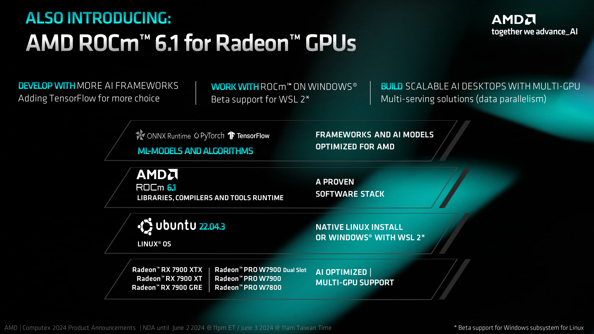
Alongside the release of the W7900DS, AMD is also promoting the upcoming Radeon release of ROCm 6.1, their software stack for GPU computing. While baseline ROCm 6.1 was introduced back in April, the Windows version of AMD’s software stack is still a trailing (and feature limited) release. So that is slated to finally get bumped up to a ROCm 6.1 release on June 19th, the same day the W7900DS launches.

ROCm 6.1 for Radeons is slated to bring a couple of major changes/improvements to the stack, particularly when it comes to expanding the scope of available features. Notably, AMD will finally be shipping Windows Subsystem for Linux 2 (WSL2) support, albeit at a beta level, allowing Windows users to access the much richer feature set and software ecosystem of ROCm under Linux. This release will also incorporate improved support for multi-GPU configurations, perfect timing for the launch of the Radeon Pro W7900DS.

Finally, ROCm 6.1 sees TensorFlow integrated into the ROCm software stack as a first-class citizen. While this matter involves more complexities than can be summarized in a simple news story, native TensorFlow support under Windows was previously blocked by a lack of a Windows version of AMD’s MIOpen machine learning library. Combined with WSL2 support, developers will have two ways to access TensorFlow on Windows systems going forward.

AMD Plans Massive Memory Instinct MI325X for Q4'24, Lays Out Accelerator Roadmap to 2026

In a packed presentation kicking off this year’s Computex trade show, AMD CEO Dr. Lisa Su spent plenty of time focusing on the subject of AI. And while the bulk of that focus was on AMD’s impending client products, the company is also currently enjoying the rapid growth of their Instinct lineup of accelerators, with the MI300 continuing to break sales projections and growth records quarter after quarter. It’s no surprise then that AMD is looking to move quickly then in the AI accelerator space, both to capitalize on the market opportunities amidst the current AI mania, as well as to stay competitive with the many chipmakers large and small who are also trying to stake a claim in the space.

To that end, as part of this evening’s announcements, AMD laid out their roadmap for their Instinct product lineup for both the short and long term, with new products and new architectures in development to carry AMD through 2026 and beyond.

On the product side of matters, AMD is announcing a new Instinct accelerator, the HBM3E-equipped MI325X. Based on the same computational silicon as the company’s MI300X accelerator, the MI325X swaps out HBM3 memory for faster and denser HBM3E, allowing AMD to produce accelerators with up to 288GB of memory, and local memory bandwidths hitting 6TB/second.

Meanwhile, AMD also showcased their first new CDNA architecture/Instinct product roadmap in two years, laying out their plans through 2026. Over the next two years AMD will be moving very quickly indeed, launching two new CDNA architectures and associated Instinct products in 2025 and 2026, respectively. The CDNA 4-powered MI350 series will be released in 2025, and that will be followed up by the even more ambitious MI400 series in 2026, which will be based on the CDNA "Next" architecture.

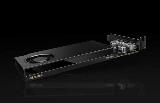
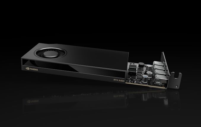
NVIDIA Intros RTX A1000 and A400: Entry-Level ProViz Cards Get Ray Tracing

With NVIDIA’s Turing architecture turning six years old this year, the company has been retiring many of the remaining Turing products from its video card lineup. And today that spirit of spring cleaning is coming to the entry-level segment of NVIDIA’s professional visualization lineup, where NVIDIA is introducing a pair of new desktop cards based on their low-end Ampere hardware.

The new RTX A1000 and RTX A400 cards will be replacing the T1000/T600/T400 lineup, which was released three years ago in 2021. The new cards slot into the same entry-level category and finally finish fleshing out the RTX A series of proviz cards, offering NVIDIA’s Ampere-generation professional graphics technologies in the lowest-power, lowest-performance, lowest-cost configuration possible.

Notably, since the entry-level T-series were based on NVIDIA’s feature-limited TU11x silicon, which lacked ray tracing and tensor core support – the basis of NVIDIA’s RTX technologies and associated branding – this marks the first time these technologies will be available in NVIDIA’s entry-level desktop proviz cards. And accordingly, these are being promoted to RTX-branded video cards, ending the odd overlap with NVIDIA’s compute cards, which never carry RTX branding.

It goes without saying that as low-end cards, the ray tracing performance of either part is nothing to write home about, but it gives NVIDIA’s current proviz lineup a consistent set of graphics features from top to bottom.

NVIDIA Professional Visualization Card Specification Comparison
  A1000 A400 T1000 T400
CUDA Cores 2304 768 896 384
Tensor Cores 72 24 N/A N/A
Boost Clock 1460MHz 1755MHz 1395MHz 1425MHz
Memory Clock 12Gbps GDDR6 12Gbps GDDR6 10Gbps GDDR6 10Gbps
GDDR6
Memory Bus Width 128-bit 64-bit 128-bit 64-bit
VRAM 8GB 4GB 8GB 4GB
Single Precision 6.74 TFLOPS 2.7 TFLOPS 2.5 TFLOPS 1.09 TFLOPS
Tensor Performance 53.8 TFLOPS 21.7 TFLOPS N/A N/A
TDP 50W 50W 50W 30W
Cooling Active, SS Active, SS Active, SS Active, SS
Outputs 4x mDP 1.4a 4x mDP 1.4a 3x mDP 1.4a
GPU GA107 TU117
Architecture Ampere Turing
Manufacturing Process Samsung 8nm TSMC 12nm
Launch Date 04/2024 05/2024 05/2021 05/2021

Both the A1000 and A400 are based on the same board design, with NVIDIA doing away with any pretense of physical feature differentiation this time around (T400 was missing its 4th Mini DisplayPort). This means both cards are based on the GA107 GPU, sporting different core and memory configurations.

RTX A1000 is a not-quite-complete configuration of GA107, with 2304 CUDA cores and 72 tensor cores. This is paired with 8GB of GDDR6, which runs at 12Gbps, for a total of 192GB/second of memory bandwidth. The TDP of the card is 50 Watts, matching its predecessor.

Meanwhile RTX A400 is far more cut down, offering about a third of the active hardware on the GPU itself, and half the memory bandwidth. On paper this gives it around 40% of T1000’s performance, and half the memory bandwidth – or 96GB/second. Notably, despite the hardware cut-down, the official TDP is still 50 Watts, versus the 30 Watts of its predecessor. So at this point NVIDIA will soon cease offering a desktop proviz card lower than 50 Watts.

As noted before, both cards otherwise feature the same physical design, with a half-height half-length (HHHL) board with active cooling. As you’d expect from such low-TDP cards, these are single-slot cooler designs. Both cards feature a quartet of Mini DisplayPorts, with the same DP 1.4a functionality that we’ve seen across all of NVIDIA’s products for the last several years.

Finally, video-focused users will want to make note that the A1000/A400 have slightly different video capabilities. While A1000 gets access to both of GA107’s NVDEC video decode blocks, A400 only gets access to a single block – one more cutback to differentiate the two cards. Otherwise, both video cards get access to the GPU’s sole NVENC block.

According to NVIDIA, the RTX A1000 will be available starting today through its distribution partners. Meanwhile the RTX A400 will hit distribution channels in May, and with OEMs expected to begin offering the cards as part of their pre-built systems this summer.

Sensor Fusion Challenges In Automotive

The number of sensors in automobiles is growing rapidly alongside new safety features and increasing levels of autonomy. The challenge is integrating them in a way that makes sense, because these sensors are optimized for different types of data, sometimes with different resolution requirements even for the same type of data, and frequently with very different latency, power consumption, and reliability requirements. Pulin Desai, group director for product marketing, management and business development at Cadence, talks about challenges with sensor fusion, the growing importance of four-dimensional sensing, what’s needed to future-proof sensor designs, and the difficulty of integrating one or more software stacks with conflicting requirements.

The post Sensor Fusion Challenges In Automotive appeared first on Semiconductor Engineering.

NVIDIA Intros RTX A1000 and A400: Entry-Level ProViz Cards Get Ray Tracing

With NVIDIA’s Turing architecture turning six years old this year, the company has been retiring many of the remaining Turing products from its video card lineup. And today that spirit of spring cleaning is coming to the entry-level segment of NVIDIA’s professional visualization lineup, where NVIDIA is introducing a pair of new desktop cards based on their low-end Ampere hardware.

The new RTX A1000 and RTX A400 cards will be replacing the T1000/T600/T400 lineup, which was released three years ago in 2021. The new cards slot into the same entry-level category and finally finish fleshing out the RTX A series of proviz cards, offering NVIDIA’s Ampere-generation professional graphics technologies in the lowest-power, lowest-performance, lowest-cost configuration possible.

Notably, since the entry-level T-series were based on NVIDIA’s feature-limited TU11x silicon, which lacked ray tracing and tensor core support – the basis of NVIDIA’s RTX technologies and associated branding – this marks the first time these technologies will be available in NVIDIA’s entry-level desktop proviz cards. And accordingly, these are being promoted to RTX-branded video cards, ending the odd overlap with NVIDIA’s compute cards, which never carry RTX branding.

It goes without saying that as low-end cards, the ray tracing performance of either part is nothing to write home about, but it gives NVIDIA’s current proviz lineup a consistent set of graphics features from top to bottom.

NVIDIA Professional Visualization Card Specification Comparison
  A1000 A400 T1000 T400
CUDA Cores 2304 768 896 384
Tensor Cores 72 24 N/A N/A
Boost Clock 1460MHz 1755MHz 1395MHz 1425MHz
Memory Clock 12Gbps GDDR6 12Gbps GDDR6 10Gbps GDDR6 10Gbps
GDDR6
Memory Bus Width 128-bit 64-bit 128-bit 64-bit
VRAM 8GB 4GB 8GB 4GB
Single Precision 6.74 TFLOPS 2.7 TFLOPS 2.5 TFLOPS 1.09 TFLOPS
Tensor Performance 53.8 TFLOPS 21.7 TFLOPS N/A N/A
TDP 50W 50W 50W 30W
Cooling Active, SS Active, SS Active, SS Active, SS
Outputs 4x mDP 1.4a 4x mDP 1.4a 3x mDP 1.4a
GPU GA107 TU117
Architecture Ampere Turing
Manufacturing Process Samsung 8nm TSMC 12nm
Launch Date 04/2024 05/2024 05/2021 05/2021

Both the A1000 and A400 are based on the same board design, with NVIDIA doing away with any pretense of physical feature differentiation this time around (T400 was missing its 4th Mini DisplayPort). This means both cards are based on the GA107 GPU, sporting different core and memory configurations.

RTX A1000 is a not-quite-complete configuration of GA107, with 2304 CUDA cores and 72 tensor cores. This is paired with 8GB of GDDR6, which runs at 12Gbps, for a total of 192GB/second of memory bandwidth. The TDP of the card is 50 Watts, matching its predecessor.

Meanwhile RTX A400 is far more cut down, offering about a third of the active hardware on the GPU itself, and half the memory bandwidth. On paper this gives it around 40% of T1000’s performance, and half the memory bandwidth – or 96GB/second. Notably, despite the hardware cut-down, the official TDP is still 50 Watts, versus the 30 Watts of its predecessor. So at this point NVIDIA will soon cease offering a desktop proviz card lower than 50 Watts.

As noted before, both cards otherwise feature the same physical design, with a half-height half-length (HHHL) board with active cooling. As you’d expect from such low-TDP cards, these are single-slot cooler designs. Both cards feature a quartet of Mini DisplayPorts, with the same DP 1.4a functionality that we’ve seen across all of NVIDIA’s products for the last several years.

Finally, video-focused users will want to make note that the A1000/A400 have slightly different video capabilities. While A1000 gets access to both of GA107’s NVDEC video decode blocks, A400 only gets access to a single block – one more cutback to differentiate the two cards. Otherwise, both video cards get access to the GPU’s sole NVENC block.

According to NVIDIA, the RTX A1000 will be available starting today through its distribution partners. Meanwhile the RTX A400 will hit distribution channels in May, and with OEMs expected to begin offering the cards as part of their pre-built systems this summer.

Intel Introduces Gaudi 3 AI Accelerator: Going Bigger and Aiming Higher In AI Market

Intel this morning is kicking off the second day of their Vision 2024 conference, the company’s annual closed-door business and customer-focused get-together. While Vision is not typically a hotbed for new silicon announcements from Intel – that’s more of an Innovation thing in the fall – attendees of this year’s show are not coming away empty handed. With a heavy focus on AI going on across the industry, Intel is using this year’s event to formally introduce the Gaudi 3 accelerator, the next-generation of Gaudi high-performance AI accelerators from Intel’s Habana Labs subsidiary.

The latest iteration of Gaudi will be launching in the third quarter of 2024, and Intel is already shipping samples to customers now. The hardware itself is something of a mixed bag in some respects (more on that in a second), but with 1835 TFLOPS of FP8 compute throughput, Intel believes it’s going to be more than enough to carve off a piece of the expansive (and expensive) AI market for themselves. Based on their internal benchmarks, the company expects to be able beat NVIDIA’s flagship Hx00 Hopper architecture accelerators in at least some critical large language models, which will open the door to Intel grabbing a larger piece of the AI accelerator market at a critical time in the industry, and a moment when there simply isn’t enough NVIDIA hardware to go around.

Introspect Intros GDDR7 Test System For Fast GDDR7 GPU Design Bring Up

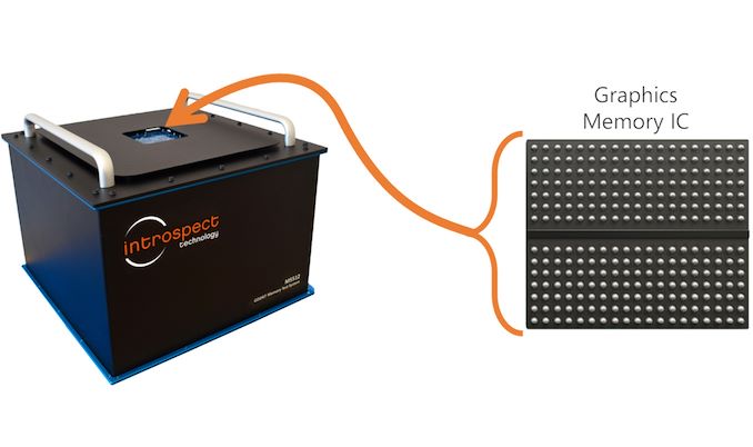
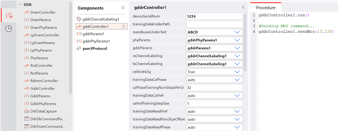
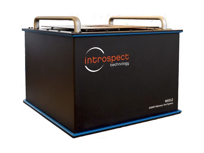
Introspect this week introduced its M5512 GDDR7 memory test system, which is designed for testing GDDR7 memory controllers, physical interface, and GDDR7 SGRAM chips. The tool will enable memory and processor manufacturers to verify that their products perform as specified by the standard.

One of the crucial phases of a processor design bring up is testing its standard interfaces, such as PCIe, DisplayPort, or GDDR is to ensure that they behave as specified both logically and electrically and achieve designated performance. Introspect's M5512 GDDR7 memory test system is designed to do just that: test new GDDR7 memory devices, troubleshoot protocol issues, assess signal integrity, and conduct comprehensive memory read/write stress tests.

The product will be quite useful for designers of GPUs/SoCs, graphics cards, PCs, network equipment and memory chips, which will speed up development of actual products that rely on GDDR7 memory. For now, GPU and SoC designers as well as memory makers use highly-custom setups consisting of many tools to characterize signal integrity as well as conduct detailed memory read/write functional stress testing, which are important things at this phase of development. But usage of a single tool greatly speeds up all the processes and gives a more comprehensive picture to specialists.

The M5512 GDDR7 Memory Test System is a desktop testing and measurement device that is equippped with 72 pins capable of functioning at up to 40 Gbps in PAM3 mode, as well as offering a virtual GDDR7 memory controller. The device features bidirectional circuitry for executing read and write operations, and every pin is equipped with an extensive range of analog characterization features, such as skew injection with femto-second resolution, voltage control with millivolt resolution, programmable jitter injection, and various eye margining features critical for AC characterization and conformance testing. Furthermore, the system integrates device power supplies with precise power sequencing and ramping controls, providing a comprehensive solution for both AC characterization and memory functional stress testing on any GDDR7 device.

Introspects M5512 has been designed in close collaboration with JEDEC members working on the GDDR7 specification, so it promises to meet all of their requirements for compliance testing. Notably, however, the device does not eliminate need for interoperability tests and still requires companies to develop their own test algorithms, but it's still a significant tool for bootstrapping device development and getting it to the point where chips can begin interop testing.

“In its quest to support the industry on GDDR7 deployment, Introspect Technology has worked tirelessly in the last few years with JEDEC members to develop the M5512 GDDR7 Memory Test System,” said Dr. Mohamed Hafed, CEO at Introspect Technology.

JEDEC Publishes GDDR7 Memory Spec: Next-Gen Graphics Memory Adds Faster PAM3 Signaling & On-Die ECC

JEDEC on Tuesday published the official specifications for GDDR7 DRAM, the latest iteration of the long-standing memory standard for graphics cards and other GPU-powered devices. The newest generation of GDDR brings a combination of memory capacity and memory bandwidth gains, with the later being driven primarily by the switch to PAM3 signaling on the memory bus. The latest graphics RAM standard also boosts the number of channels per DRAM chip, adds new interface training patterns, and brings in on-die ECC to maintain the effective reliability of the memory.

“JESD239 GDDR7 marks a substantial advancement in high-speed memory design,” said Mian Quddus, JEDEC Board of Directors Chairman. “With the shift to PAM3 signaling, the memory industry has a new path to extend the performance of GDDR devices and drive the ongoing evolution of graphics and various high-performance applications.”

GDDR7 has been in development for a few years now, with JEDEC members making the first disclosures around the memory technology about a year ago, when Cadence revealed the use of PAM3 encoding as part of their validation tools. Since then we've heard from multiple memory manufacturers that we should expect the final version of the memory to launch in 2024, with JEDEC's announcement essentially coming right on schedule.

As previously revealed, the biggest technical change with GDDR7 comes with the switch from two-bit non-return-to-zero (NRZ) encoding on the memory bus to three-bit pulse amplitude modulating (PAM3) encoding. This change allows GDDR7 to transmit 3 bits over two cycles, 50% more data than GDDR6 operating at an identical clockspeed. As a result, GDDR7 can support higher overall data transfer rates, the critical component to making each generation of GDDR successively faster than its predecessor.

GDDR Generations
  GDDR7 GDDR6X
(Non-JEDEC)
GDDR6
B/W Per Pin 32 Gbps (Gen 1)
48 Gbps (Spec Max)
24 Gbps (Shipping) 24 Gbps (Sampling)
Chip Density 2 GB (16 Gb) 2 GB (16 Gb) 2 GB (16 Gb)
Total B/W (256-bit bus) 1024 GB/sec 768 GB/sec 768 GB/sec
DRAM Voltage 1.2 V 1.35 V 1.35 V
Data Rate QDR QDR QDR
Signaling PAM-3 PAM-4 NRZ (Binary)
Maximum Density 64 Gb 32 Gb 32 Gb
Packaging 266 FBGA 180 FBGA 180 FBGA

The first generation of GDDR7 is expected to run at data rates around 32 Gbps per pin, and memory manufacturers have previously talked about rates up to 36 Gbps/pin as being easily attainable. However the GDDR7 standard itself leaves room for even higher data rates – up to 48 Gbps/pin – with JEDEC going so far as touting GDDR7 memory chips "reaching up to 192 GB/s [32b @ 48Gbps] per device" in their press release. Notably, this is a significantly higher increase in bandwidth than what PAM3 signaling brings on its own, which means there are multiple levels of enhancements within GDDR7's design.

Digging deeper into the specification, JEDEC has also once again subdivided a single 32-bit GDDR memory chip into a larger number of channels. Whereas GDDR6 offered two 16-bit channels, GDDR7 expands this to four 8-bit channels. The distinction is somewhat arbitrary from an end-user's point of view – it's still a 32-bit chip operating at 32Gbps/pin regardless – but it has a great deal of impact on how the chip works internally. Especially as JEDEC has kept the 256-bit per channel prefetch of GDDR5 and GDDR6, making GDDR7 a 32n prefetch design.
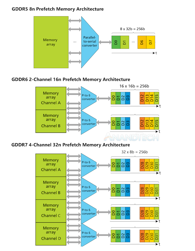

GDDR Channel Architecture. Original GDDR6-era Diagram Courtesy Micron

The net impact of all of this is that, by halving the channel width but keeping the prefetch size the same, JEDEC has effectively doubled the amount of data that is prefetched per cycle of the DRAM cells. This is a pretty standard trick to extend the bandwidth of DRAM memory, and is essentially the same thing JEDEC did with GDDR6 in 2018. But it serves as a reminder that DRAM cells are still very slow (on the order of hundreds of MHz) and aren't getting any faster. So the only way to feed faster memory buses is by fetching ever-larger amounts of data in a single go.

The change in the number of channels per memory chip also has a minor impact on how multi-channel "clamshell" mode works for higher capacity memory configurations. Whereas GDDR6 accessed a single memory channel from each chip in a clamshell configuration, GDDR7 will access two channels – what JEDEC is calling two-channel mode. Specifically, this mode reads channels A and C from each chip. It is effectively identical to how clamshell mode behaved with GDDR6, and it means that while clamshell configurations remain supported in this latest generation of memory, there aren't any other tricks being employed to improve memory capacity beyond ever-increasing memory chip densities.

On that note, the GDDR7 standard officially adds support for 64Gbit DRAM devices, twice the 32Gbit max capacity of GDDR6/GDDR6X. Non-power-of-two capacities continue to be supported as well, allowing for 24Gbit and 48Gbit chips. Support for larger memory chips further pushes the maximum memory capacity of a theoretical high-end video card with a 384-bit memory bus to as high as 192GB of memory – a development that would no doubt be welcomed by datacenter operators in the era of large language AI models. With that said, however, we're still regularly seeing 16Gbit memory chips used on today's memory cards, even though GDDR6 supports 32Gbit chips. Coupled with the fact that Samsung and Micron have already disclosed that their first generation of GDDR7 chips will also top out at 16Gbit/24Gbit respectively, it's safe to say that 64Gbit chips are pretty far off in the future right now (so don't sell off your 48GB cards quite yet).

For their latest generation of memory technology, JEDEC is also including several new-to-GDDR memory reliability features. Most notably, on-die ECC capabilities, similar to what we saw with the introduction of DDR5. And while we haven't been able to get an official comment from JEDEC on why they've opted to include ECC support now, its inclusion is not surprising given the reliability requirements for DDR5. In short, as memory chip densities have increased, it has become increasingly hard to yield a "perfect" die with no flaws; so adding on-chip ECC allows memory manufacturers to keep their chips operating reliably in the face of unavoidable errors.
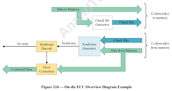

This figure is reproduced, with permission, from JEDEC document JESD239, figure 124

Internally, the GDDR7 spec requires a minimum of 16 bits of parity data per 256 bits of user data (6.25%), with JEDEC giving an example implementation of a 9-bit single error correcting code (SEC) plus a 7-bit cyclic redundancy check (CRC). Overall, GDDR7 on-die ECC should be able to correct 100% of 1-bit errors, and detect 100% of 2-bit errors – falling to 99.3% in the rare case of 3-bit errors. Information about memory errors is also made available to the memory controller, via what JEDEC terms their on-die ECC transparency protocol. And while technically separate from ECC itself, GDDR7 also throws in another memory reliability feature with command address parity with command blocking (CAPARBLK), which is intended to improve the integrity of the command address bus.

Otherwise, while the inclusion of on-die ECC isn't likely to have any more of an impact on consumer video cards than its inclusion had for DDR5 memory and consumer platforms there, it remains to be seen what this will mean for workstation and server video cards. The vendors there have used soft ECC on top of unprotected memory for several generations now; presumably this will remain the case for GDDR7 cards as well, but the regular use of soft ECC makes things a lot more flexible than in the CPU space.
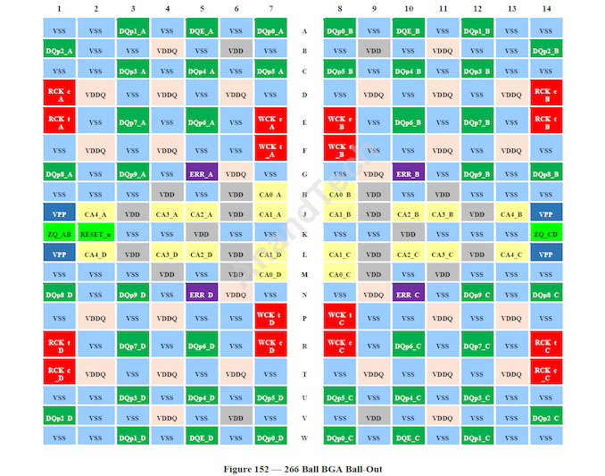

This figure is reproduced, with permission, from JEDEC document JESD239, figure 152

Finally, GDDR7 is also introducing a suite of other reliability-related features, primarily related to helping PAM3 operation. This includes core independent LFSR (linear-feedback shift register) training patterns with eye masking and error counters. LFSR training patterns are used to test and adjust the interface (to ensure efficiency), eye masking evaluates signal quality, and error counters track the number of errors during training.

Technical matters aside, this week's announcement includes statements of support from all of the usual players on both sides of the isle, including AMD and NVIDA, and the Micron/Samsung/SKhynix trifecta. It goes without saying that all parties are keen to getting to use or sell GDDR7 respectively, given the memory capacity and bandwidth improvements it will bring – and especially in this era where anything aimed at the AI market is selling like hotcakes.

No specific products are being announced at this time, but with Samsung and Micron having previously announced their intentions to ship GDDR7 memory this year, we should see new memory (and new GPUs to pair it with) later this year.

JEDEC standards and publications are copyrighted by the JEDEC Solid State Technology Association.  All rights reserved.

Palit Releases Fanless Version of NVIDIA's New GeForce RTX 3050 6GB

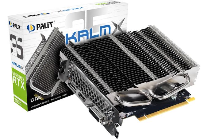
NVIDIA today is quietly launching a new entry-level graphics card for the retail market, the GeForce RTX 3050 6GB. Based on a cut-down version of their budget Ampere-architecture GA107 GPU, the new card brings what was previously an OEM-only product to the retail market. Besides adding another part to NVIDIA's deep product stack, the launch of the RTX 3050 6GB also comes with another perk: lower power consumption thanks to this part targeting system installs where an external PCIe power connector would not be needed. NVIDIA's partners, in turn, have not wasted any time in taking advantage of this, and today Palit is releasing its first fanless KalmX board in years: the GeForce RTX 3050 KalmX 6GB.
The GeForce RTX 3050 6GB is based on the GA107 graphics processor with 2304 CUDA cores, which is paired with 6GB of GDDR6 attached to a petite 96-bit memory bus (versus 128-bit for the full RTX 3050 8GB). Coupled with a boost clock rating of just 1470 MHz, the RTX 3050 6GB delivers tangibly lower compute performance than the fully-fledged RTX 3050 — 6.77 FP32 TFLOPS vs 9.1 FP32 TFLOPS — but these compromises offer an indisputable advantage: a 70W power target.

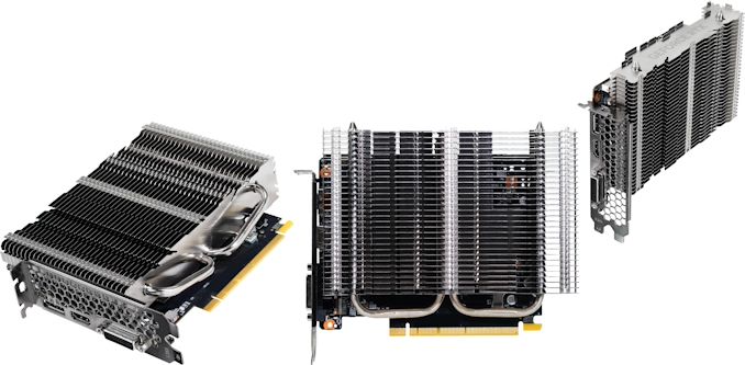
Palit is the first company that takes advantage of this reduced power consumption of the GeForce RTX 3050 6 GB, as the company has launched a passively cooled graphics card based on this part, the first in four years. The Palit GeForce RTX 3050 KalmX 6GB (NE63050018JE-1170H) uses a custom printed circuit board (PCB) that not only offers modern DisplayPort 1.4a and HDMI 2.1 outputs, but, as we still see in some entry-level cards, a dual-link DVI-D connector (a first for an Ampere-based graphics card).

The dual-slot passive cooling system with two heat pipes is certainly the main selling point of Palit's GeForce RTX 3050 KalmX 6GB. The product is pretty large though — it measures 166.3×137×38.3 mm — and will not fit into tiny desktops. Still, given the fact that fanless systems are usually not the most compact ones, this may not be a significant limitation of the new KalmX device.

Another advantage of Palit's GeForce RTX 3050 KalmX 6GB in particular and NVIDIA's GeForce RTX 3050 6GB in general is that it can be powered entirely via a PCIe slot, which eliminates the need for an auxiliary PCIe power connectors (which are sometimes not present in cheap systems from big OEMs).

Wccftech reports that NVIDIA's GeForce RTX 3050 6GB graphics cards will carry a recommended price tag of $169 and indeed these cards are available for $170 - $180. This looks to be a quite competitive price point as the product offers higher compute performance than that of AMD's Radeon RX 6400 ($125) and Radeon RX 6500 XT ($140). Meanwhile, it remains to be seen how much will Palit charge for its uniquely positioned GeForce RTX 3050 KalmX 6GB.

Palit Releases Fanless Version of NVIDIA's New GeForce RTX 3050 6GB

NVIDIA today is quietly launching a new entry-level graphics card for the retail market, the GeForce RTX 3050 6GB. Based on a cut-down version of their budget Ampere-architecture GA107 GPU, the new card brings what was previously an OEM-only product to the retail market. Besides adding another part to NVIDIA's deep product stack, the launch of the RTX 3050 6GB also comes with another perk: lower power consumption thanks to this part targeting system installs where an external PCIe power connector would not be needed. NVIDIA's partners, in turn, have not wasted any time in taking advantage of this, and today Palit is releasing its first fanless KalmX board in years: the GeForce RTX 3050 KalmX 6GB.
The GeForce RTX 3050 6GB is based on the GA107 graphics processor with 2304 CUDA cores, which is paired with 6GB of GDDR6 attached to a petite 96-bit memory bus (versus 128-bit for the full RTX 3050 8GB). Coupled with a boost clock rating of just 1470 MHz, the RTX 3050 6GB delivers tangibly lower compute performance than the fully-fledged RTX 3050 — 6.77 FP32 TFLOPS vs 9.1 FP32 TFLOPS — but these compromises offer an indisputable advantage: a 70W power target.

Palit is the first company that takes advantage of this reduced power consumption of the GeForce RTX 3050 6 GB, as the company has launched a passively cooled graphics card based on this part, the first in four years. The Palit GeForce RTX 3050 KalmX 6GB (NE63050018JE-1170H) uses a custom printed circuit board (PCB) that not only offers modern DisplayPort 1.4a and HDMI 2.1 outputs, but, as we still see in some entry-level cards, a dual-link DVI-D connector (a first for an Ampere-based graphics card).

The dual-slot passive cooling system with two heat pipes is certainly the main selling point of Palit's GeForce RTX 3050 KalmX 6GB. The product is pretty large though — it measures 166.3×137×38.3 mm — and will not fit into tiny desktops. Still, given the fact that fanless systems are usually not the most compact ones, this may not be a significant limitation of the new KalmX device.

Another advantage of Palit's GeForce RTX 3050 KalmX 6GB in particular and NVIDIA's GeForce RTX 3050 6GB in general is that it can be powered entirely via a PCIe slot, which eliminates the need for an auxiliary PCIe power connectors (which are sometimes not present in cheap systems from big OEMs).

Wccftech reports that NVIDIA's GeForce RTX 3050 6GB graphics cards will carry a recommended price tag of $169 and indeed these cards are available for $170 - $180. This looks to be a quite competitive price point as the product offers higher compute performance than that of AMD's Radeon RX 6400 ($125) and Radeon RX 6500 XT ($140). Meanwhile, it remains to be seen how much will Palit charge for its uniquely positioned GeForce RTX 3050 KalmX 6GB.

❌