FreshRSS

Zobrazení pro čtení

Jsou dostupné nové články, klikněte pro obnovení stránky.

Scientists observe record-setting electron mobility in a new crystal film

A material with a high electron mobility is like a highway without traffic. Any electrons that flow into the material experience a commuter’s dream, breezing through without any obstacles or congestion to slow or scatter them off their path.

The higher a material’s electron mobility, the more efficient its electrical conductivity, and the less energy is lost or wasted as electrons zip through. Advanced materials that exhibit high electron mobility will be essential for more efficient and sustainable electronic devices that can do more work with less power.

Now, physicists at MIT, the Army Research Lab, and elsewhere have achieved a record-setting level of electron mobility in a thin film of ternary tetradymite — a class of mineral that is naturally found in deep hydrothermal deposits of gold and quartz.

For this study, the scientists grew pure, ultrathin films of the material, in a way that minimized defects in its crystalline structure. They found that this nearly perfect film — much thinner than a human hair — exhibits the highest electron mobility in its class.

The team was able to estimate the material’s electron mobility by detecting quantum oscillations when electric current passes through. These oscillations are a signature of the quantum mechanical behavior of electrons in a material. The researchers detected a particular rhythm of oscillations that is characteristic of high electron mobility — higher than any ternary thin films of this class to date.

“Before, what people had achieved in terms of electron mobility in these systems was like traffic on a road under construction — you’re backed up, you can’t drive, it’s dusty, and it’s a mess,” says Jagadeesh Moodera, a senior research scientist in MIT’s Department of Physics. “In this newly optimized material, it’s like driving on the Mass Pike with no traffic.”

The team’s results, which appear today in the journal Materials Today Physics, point to ternary tetradymite thin films as a promising material for future electronics, such as wearable thermoelectric devices that efficiently convert waste heat into electricity. (Tetradymites are the active materials that cause the cooling effect in commercial thermoelectric coolers.) The material could also be the basis for spintronic devices, which process information using an electron’s spin, using far less power than conventional silicon-based devices.

The study also uses quantum oscillations as a highly effective tool for measuring a material’s electronic performance.

“We are using this oscillation as a rapid test kit,” says study author Hang Chi, a former research scientist at MIT who is now at the University of Ottawa. “By studying this delicate quantum dance of electrons, scientists can start to understand and identify new materials for the next generation of technologies that will power our world.”

Chi and Moodera’s co-authors include Patrick Taylor, formerly of MIT Lincoln Laboratory, along with Owen Vail and Harry Hier of the Army Research Lab, and Brandi Wooten and Joseph Heremans of Ohio State University.

Beam down

The name “tetradymite” derives from the Greek “tetra” for “four,” and “dymite,” meaning “twin.” Both terms describe the mineral’s crystal structure, which consists of rhombohedral crystals that are “twinned” in groups of four — i.e. they have identical crystal structures that share a side.

Tetradymites comprise combinations of bismuth, antimony tellurium, sulfur, and selenium. In the 1950s, scientists found that tetradymites exhibit semiconducting properties that could be ideal for thermoelectric applications: The mineral in its bulk crystal form was able to passively convert heat into electricity.

Then, in the 1990s, the late Institute Professor Mildred Dresselhaus proposed that the mineral’s thermoelectric properties might be significantly enhanced, not in its bulk form but within its microscopic, nanometer-scale surface, where the interactions of electrons is more pronounced. (Heremans happened to work in Dresselhaus’ group at the time.)

“It became clear that when you look at this material long enough and close enough, new things will happen,” Chi says. “This material was identified as a topological insulator, where scientists could see very interesting phenomena on their surface. But to keep uncovering new things, we have to master the material growth.”

To grow thin films of pure crystal, the researchers employed molecular beam epitaxy — a method by which a beam of molecules is fired at a substrate, typically in a vacuum, and with precisely controlled temperatures. When the molecules deposit on the substrate, they condense and build up slowly, one atomic layer at a time. By controlling the timing and type of molecules deposited, scientists can grow ultrathin crystal films in exact configurations, with few if any defects.

“Normally, bismuth and tellurium can interchange their position, which creates defects in the crystal,” co-author Taylor explains. “The system we used to grow these films came down with me from MIT Lincoln Laboratory, where we use high purity materials to minimize impurities to undetectable limits. It is the perfect tool to explore this research.”

Free flow

The team grew thin films of ternary tetradymite, each about 100 nanometers thin. They then tested the film’s electronic properties by looking for Shubnikov-de Haas quantum oscillations — a phenomenon that was discovered by physicists Lev Shubnikov and Wander de Haas, who found that a material’s electrical conductivity can oscillate when exposed to a strong magnetic field at low temperatures. This effect occurs because the material’s electrons fill up specific energy levels that shift as the magnetic field changes.

Such quantum oscillations could serve as a signature of a material’s electronic structure, and the ways in which electrons behave and interact. Most notably for the MIT team, the oscillations could determine a material’s electron mobility: If oscillations exist, it must mean that the material’s electrical resistance is able to change, and by inference, electrons can be mobile, and made to easily flow.

The team looked for signs of quantum oscillations in their new films, by first exposing them to ultracold temperatures and a strong magnetic field, then running an electric current through the film and measuring the voltage along its path, as they tuned the magnetic field up and down.

“It turns out, to our great joy and excitement, that the material’s electrical resistance oscillates,” Chi says. “Immediately, that tells you that this has very high electron mobility.”

Specifically, the team estimates that the ternary tetradymite thin film exhibits an electron mobility of 10,000 cm2/V-s — the highest mobility of any ternary tetradymite film yet measured. The team suspects that the film’s record mobility has something to do with its low defects and impurities, which they were able to minimize with their precise growth strategies. The fewer a material’s defects, the fewer obstacles an electron encounters, and the more freely it can flow.

“This is showing it’s possible to go a giant step further, when properly controlling these complex systems,” Moodera says. “This tells us we’re in the right direction, and we have the right system to proceed further, to keep perfecting this material down to even much thinner films and proximity coupling for use in future spintronics and wearable thermoelectric devices.”

This research was supported in part by the Army Research Office, National Science Foundation, Office of Naval Research, Canada Research Chairs Program and Natural Sciences and Engineering Research Council of Canada.

© Credit: Courtesy of the researchers; edited by MIT News

Researchers have grown thin films of ternary tetradymite (shown) that exhibit record high electron mobility.

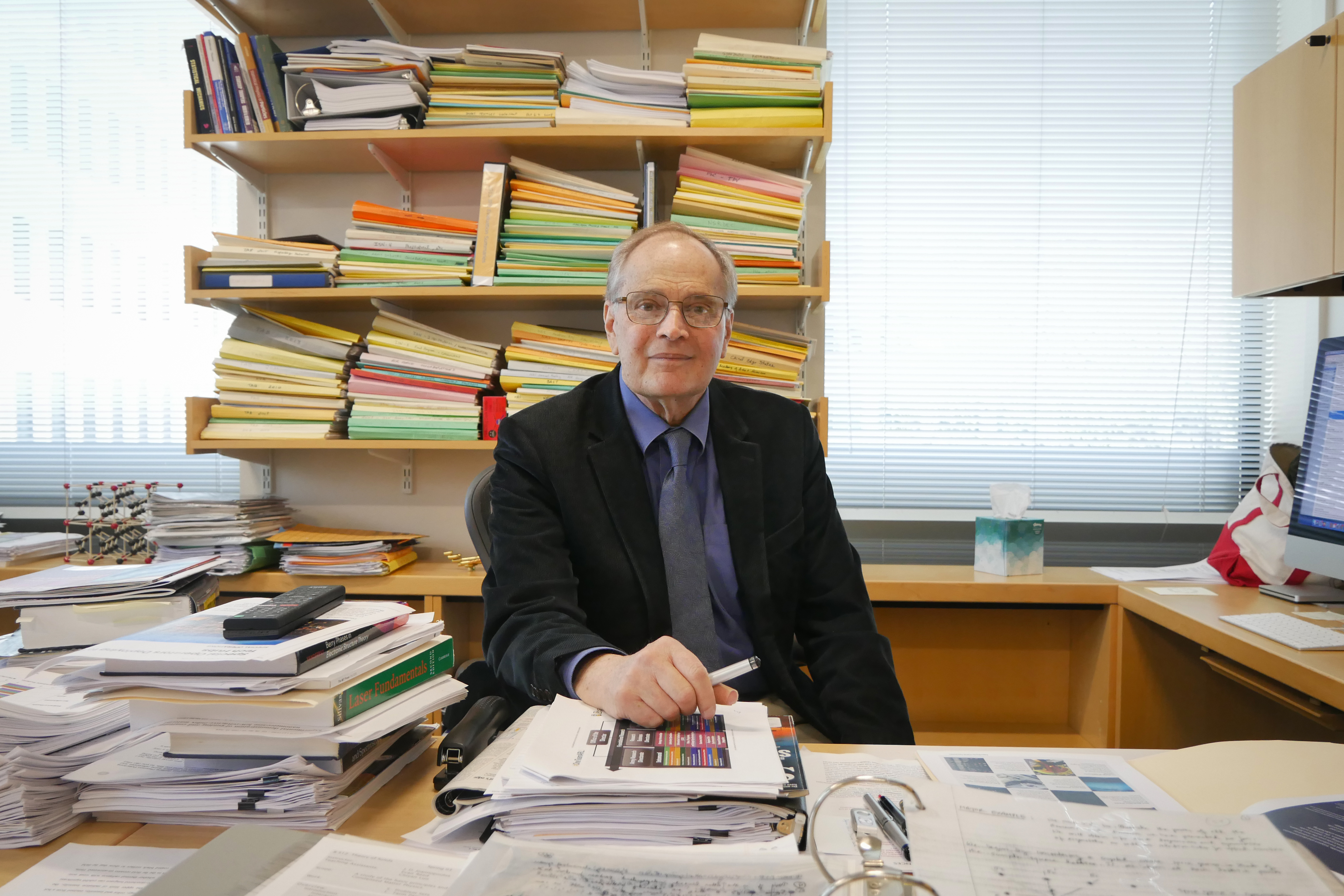
John Joannopoulos receives 2024-2025 Killian Award

John Joannopoulos, an innovator and mentor in the fields of theoretical condensed matter physics and nanophotonics, has been named the recipient of the 2024-2025 James R. Killian Jr. Faculty Achievement Award.

Joannopoulos is the Francis Wright Davis Professor of Physics and director of MIT’s Institute for Soldier Nanotechnologies. He has been a member of the MIT faculty for 50 years.

“Professor Joannopoulos’s profound and lasting impact on the field of theoretical condensed matter physics finds its roots in his pioneering work in harnessing ab initio physics to elucidate the behavior of materials at the atomic level,” states the award citation, which was announced at today’s faculty meeting by Roger White, chair of the Killian Award Selection Committee and professor of philosophy at MIT. “His seminal research in the development of photonic crystals has revolutionized understanding of light-matter interactions, laying the groundwork for transformative advancements in diverse fields ranging from telecommunications to biomedical engineering.”

The award also honors Joannopoulos’ service as a “legendary mentor to generations of students, inspiring them to achieve excellence in science while at the same time facilitating the practical benefit to society through entrepreneurship.”

The Killian Award was established in 1971 to recognize outstanding professional contributions by MIT faculty members. It is the highest honor that the faculty can give to one of its members.

“I have to tell you, it was a complete and utter surprise,” Joannopoulos told MIT News shortly after he received word of the award. “I didn’t expect it at all, and was extremely flattered, honored, and moved by it, frankly.”

Joannopoulous has spent his entire professional career at MIT. He came to the Institute in 1974, directly after receiving his PhD in physics at the University of California at Berkeley, where he also earned his bachelor’s degree. Starting out as an assistant professor in MIT’s Department of Physics, he quickly set up a research program focused on theoretical condensed matter physics.

Over the first half of his MIT career, Joannopoulos worked to elucidate the fundamental nature of the electronic, vibrational, and optical structure of crystalline and amorphous bulk solids, their surfaces, interfaces, and defects. He and his students developed numerous theoretical methods to enable tractable and accurate calculations of these complex systems.

In the 1990s, his work with microscopic material systems expanded to a new class of materials, called photonic crystals — materials that could be engineered at the micro- and nanoscale to manipulate light in ways that impart surprising and exotic optical qualities to the material as a whole.

“I saw that you could create photonic crystals with defects that can affect the properties of photons, in much the same way that defects in a semiconductor affect the properties of electrons,” Joannopoulos says. “So I started working in this area to try and explore what anomalous light phenomena can we discover using this approach?”

Among his various breakthroughs in the field was the realization of a “perfect dielectric mirror” — a multilayered optical device that reflects light from all angles as normal metallic mirrors do, and that can also be tuned to reflect and trap light at specific frequencies. He and his colleagues saw potential for the mirror to be made into a hollow fiber that could serve as a highly effective optical conduit, for use in a wide range of applications. To further advance the technology, he and his colleagues launched a startup, which has since developed the technology into a flexible, fiber-optic “surgical scalpel.”

Throughout his career, Joannopoulos has helped to launch numerous startups and photonics-based technologies.

“His ability to bridge the gap between academia and industry has not only advanced scientific knowledge but also led to the creation of dozens of new companies, thousands of jobs, and groundbreaking products that continue to benefit society to this day,” the award citation states.

In 2006, Joannopoulos accepted the position as director of MIT’s Institute for Soldier Nanotechnologies (ISN), a collaboration between MIT researchers, industry partners, and military defense experts, who seek innovations to protect and enhance soldiers’ survivability in the field. In his role as ISN head, Joannopoulos has worked across MIT, making connections and supporting new projects with researchers specializing in fields far from his own.

“I get a chance to explore and learn fascinating new things,” says Joannopoulos, who is currently overseeing projects related to hyperspectral imaging, smart and responsive fabrics, and nanodrug delivery. “I love that aspect of really getting to understand what people in other fields are doing. And they’re doing great work across many, many different fields.”

Throughout his career at MIT, Joannopoulos has been especially inspired and motivated by his students, many of whom have gone on to found companies, lead top academic and research institutions, and make significant contributions to their respective fields, including one student who was awarded the Nobel Prize in Physics in 1998.

“One’s proudest moments are the successes of one’s students, and in that regard, I’ve been extremely lucky to have had truly exceptional students over the years,” Joannopolous says.

His many contributions to academia and industry have earned Joannopoulos numerous honors and awards, including his election to both the National Academy of Sciences and the American Academy of Arts and Sciences. He is also a fellow of both the American Physical Society and the American Association for the Advancement of Science.

“The Selection Committee is delighted to have this opportunity to honor Professor John Joannopoulos: a visionary scientist, a beloved mentor, a great believer in the goodness of people, and a leader whose contributions to MIT and the broader scientific community are immeasurable,” the award citation concludes.

© Photo: Jose-Luis Olivares, MIT

Physicists arrange atoms in extremely close proximity

Proximity is key for many quantum phenomena, as interactions between atoms are stronger when the particles are close. In many quantum simulators, scientists arrange atoms as close together as possible to explore exotic states of matter and build new quantum materials.

They typically do this by cooling the atoms to a stand-still, then using laser light to position the particles as close as 500 nanometers apart — a limit that is set by the wavelength of light. Now, MIT physicists have developed a technique that allows them to arrange atoms in much closer proximity, down to a mere 50 nanometers. For context, a red blood cell is about 1,000 nanometers wide.

The physicists demonstrated the new approach in experiments with dysprosium, which is the most magnetic atom in nature. They used the new approach to manipulate two layers of dysprosium atoms, and positioned the layers precisely 50 nanometers apart. At this extreme proximity, the magnetic interactions were 1,000 times stronger than if the layers were separated by 500 nanometers.

What’s more, the scientists were able to measure two new effects caused by the atoms’ proximity. Their enhanced magnetic forces caused “thermalization,” or the transfer of heat from one layer to another, as well as synchronized oscillations between layers. These effects petered out as the layers were spaced farther apart.

“We have gone from positioning atoms from 500 nanometers to 50 nanometers apart, and there is a lot you can do with this,” says Wolfgang Ketterle, the John D. MacArthur Professor of Physics at MIT. “At 50 nanometers, the behavior of atoms is so much different that we’re really entering a new regime here.”

Ketterle and his colleagues say the new approach can be applied to many other atoms to study quantum phenomena. For their part, the group plans to use the technique to manipulate atoms into configurations that could generate the first purely magnetic quantum gate — a key building block for a new type of quantum computer.

The team has published their results today in the journal Science. The study’s co-authors include lead author and physics graduate student Li Du, along with Pierre Barral, Michael Cantara, Julius de Hond, and Yu-Kun Lu — all members of the MIT-Harvard Center for Ultracold Atoms, the Department of Physics, and the Research Laboratory of Electronics at MIT.

Peaks and valleys

To manipulate and arrange atoms, physicists typically first cool a cloud of atoms to temperatures approaching absolute zero, then use a system of laser beams to corral the atoms into an optical trap.

Laser light is an electromagnetic wave with a specific wavelength (the distance between maxima of the electric field) and frequency. The wavelength limits the smallest pattern into which light can be shaped to typically 500 nanometers, the so-called optical resolution limit. Since atoms are attracted by laser light of certain frequencies, atoms will be positioned at the points of peak laser intensity. For this reason, existing techniques have been limited in how close they can position atomic particles, and could not be used to explore phenomena that happen at much shorter distances.

“Conventional techniques stop at 500 nanometers, limited not by the atoms but by the wavelength of light,” Ketterle explains. “We have found now a new trick with light where we can break through that limit.”

The team’s new approach, like current techniques, starts by cooling a cloud of atoms — in this case, to about 1 microkelvin, just a hair above absolute zero — at which point, the atoms come to a near-standstill. Physicists can then use lasers to move the frozen particles into desired configurations.

Then, Du and his collaborators worked with two laser beams, each with a different frequency, or color, and circular polarization, or direction of the laser’s electric field. When the two beams travel through a super-cooled cloud of atoms, the atoms can orient their spin in opposite directions, following either of the two lasers’ polarization. The result is that the beams produce two groups of the same atoms, only with opposite spins.

Each laser beam formed a standing wave, a periodic pattern of electric field intensity with a spatial period of 500 nanometers. Due to their different polarizations, each standing wave attracted and corralled one of two groups of atoms, depending on their spin. The lasers could be overlaid and tuned such that the distance between their respective peaks is as small as 50 nanometers, meaning that the atoms gravitating to each respective laser’s peaks would be separated by the same 50 nanometers.

But in order for this to happen, the lasers would have to be extremely stable and immune to all external noise, such as from shaking or even breathing on the experiment. The team realized they could stabilize both lasers by directing them through an optical fiber, which served to lock the light beams in place in relation to each other.

“The idea of sending both beams through the optical fiber meant the whole machine could shake violently, but the two laser beams stayed absolutely stable with respect to each others,” Du says.

Magnetic forces at close range

As a first test of their new technique, the team used atoms of dysprosium — a rare-earth metal that is one of the strongest magnetic elements in the periodic table, particularly at ultracold temperatures. However, at the scale of atoms, the element’s magnetic interactions are relatively weak at distances of even 500 nanometers. As with common refrigerator magnets, the magnetic attraction between atoms increases with proximity, and the scientists suspected that if their new technique could space dysprosium atoms as close as 50 nanometers apart, they might observe the emergence of otherwise weak interactions between the magnetic atoms.

“We could suddenly have magnetic interactions, which used to be almost neglible but now are really strong,” Ketterle says.

The team applied their technique to dysprosium, first super-cooling the atoms, then passing two lasers through to split the atoms into two spin groups, or layers. They then directed the lasers through an optical fiber to stabilize them, and found that indeed, the two layers of dysprosium atoms gravitated to their respective laser peaks, which in effect separated the layers of atoms by 50 nanometers — the closest distance that any ultracold atom experiment has been able to achieve.

At this extremely close proximity, the atoms’ natural magnetic interactions were significantly enhanced, and were 1,000 times stronger than if they were positioned 500 nanometers apart. The team observed that these interactions resulted in two novel quantum phenomena: collective oscillation, in which one layer’s vibrations caused the other layer to vibrate in sync; and thermalization, in which one layer transferred heat to the other, purely through magnetic fluctuations in the atoms.

“Until now, heat between atoms could only by exchanged when they were in the same physical space and could collide,” Du notes. “Now we have seen atomic layers, separated by vacuum, and they exchange heat via fluctuating magnetic fields.”

The team’s results introduce a new technique that can be used to position many types of atom in close proximity. They also show that atoms, placed close enough together, can exhibit interesting quantum phenomena, that could be harnessed to build new quantum materials, and potentially, magnetically-driven atomic systems for quantum computers.

“We are really bringing super-resolution methods to the field, and it will become a general tool for doing quantum simulations,” Ketterle says. “There are many variants possible, which we are working on.”

This research was funded, in part, by the National Science Foundation and the Department of Defense.

© Image: Courtesy of the researchers; MIT News

MIT physicists developed a technique to arrange atoms (represented as spheres with arrows) in much closer proximity than previously possible, down to 50 nanometers. The group plans to use the method to manipulate atoms into configurations that could generate the first purely magnetic quantum gate — a key building block for a new type of quantum computer. In this image, the magnetic interaction is represented by the colorful lines.

“Nanostitches” enable lighter and tougher composite materials

To save on fuel and reduce aircraft emissions, engineers are looking to build lighter, stronger airplanes out of advanced composites. These engineered materials are made from high-performance fibers that are embedded in polymer sheets. The sheets can be stacked and pressed into one multilayered material and made into extremely lightweight and durable structures.

But composite materials have one main vulnerability: the space between layers, which is typically filled with polymer “glue” to bond the layers together. In the event of an impact or strike, cracks can easily spread between layers and weaken the material, even though there may be no visible damage to the layers themselves. Over time, as these hidden cracks spread between layers, the composite could suddenly crumble without warning.

Now, MIT engineers have shown they can prevent cracks from spreading between composite’s layers, using an approach they developed called “nanostitching,” in which they deposit chemically grown microscopic forests of carbon nanotubes between composite layers. The tiny, densely packed fibers grip and hold the layers together, like ultrastrong Velcro, preventing the layers from peeling or shearing apart.

In experiments with an advanced composite known as thin-ply carbon fiber laminate, the team demonstrated that layers bonded with nanostitching improved the material’s resistance to cracks by up to 60 percent, compared with composites with conventional polymers. The researchers say the results help to address the main vulnerability in advanced composites.

“Just like phyllo dough flakes apart, composite layers can peel apart because this interlaminar region is the Achilles’ heel of composites,” says Brian Wardle, professor of aeronautics and astronautics at MIT. “We’re showing that nanostitching makes this normally weak region so strong and tough that a crack will not grow there. So, we could expect the next generation of aircraft to have composites held together with this nano-Velcro, to make aircraft safer and have greater longevity.”

Wardle and his colleagues have published their results today in the journal ACS Applied Materials and Interfaces. The study’s first author is former MIT visiting graduate student and postdoc Carolina Furtado, along with Reed Kopp, Xinchen Ni, Carlos Sarrado, Estelle Kalfon-Cohen, and Pedro Camanho.

Forest growth

At MIT, Wardle is director of the necstlab (pronounced “next lab”), where he and his group first developed the concept for nanostitching. The approach involves “growing” a forest of vertically aligned carbon nanotubes — hollow fibers of carbon, each so small that tens of billions of the the nanotubes can stand in an area smaller than a fingernail. To grow the nanotubes, the team used a process of chemical vapor deposition to react various catalysts in an oven, causing carbon to settle onto a surface as tiny, hair-like supports. The supports are eventually removed, leaving behind a densely packed forest of microscopic, vertical rolls of carbon.

The lab has previously shown that the nanotube forests can be grown and adhered to layers of composite material, and that this fiber-reinforced compound improves the material’s overall strength. The researchers had also seen some signs that the fibers can improve a composite’s resistance to cracks between layers.

In their new study, the engineers took a more in-depth look at the between-layer region in composites to test and quantify how nanostitching would improve the region’s resistance to cracks. In particular, the study focused on an advanced composite material known as thin-ply carbon fiber laminates.

“This is an emerging composite technology, where each layer, or ply, is about 50 microns thin, compared to standard composite plies that are 150 microns, which is about the diameter of a human hair. There’s evidence to suggest they are better than standard-thickness composites. And we wanted to see whether there might be synergy between our nanostitching and this thin-ply technology, since it could lead to more resilient aircraft, high-value aerospace structures, and space and military vehicles,” Wardle says.

Velcro grip

The study’s experiments were led by Carolina Furtado, who joined the effort as part of the MIT-Portugal program in 2016, continued the project as a postdoc, and is now a professor at the University of Porto in Portugal, where her research focuses on modeling cracks and damage in advanced composites.

In her tests, Furtado used the group’s techniques of chemical vapor deposition to grow densely packed forests of vertically aligned carbon nanotubes. She also fabricated samples of thin-ply carbon fiber laminates. The resulting advanced composite was about 3 millimeters thick and comprised 60 layers, each made from stiff, horizontal fibers embedded in a polymer sheet.

She transferred and adhered the nanotube forest in between the two middle layers of the composite, then cooked the material in an autoclave to cure. To test crack resistance, the researchers placed a crack on the edge of the composite, right at the start of the region between the two middle layers.

“In fracture testing, we always start with a crack because we want to test whether and how far the crack will spread,” Furtado explains.

The researchers then placed samples of the nanotube-reinforced composite in an experimental setup to test their resilience to “delamination,” or the potential for layers to separate.

“There’s lots of ways you can get precursors to delamination, such as from impacts, like tool drop, bird strike, runway kickup in aircraft, and there could be almost no visible damage, but internally it has a delamination,” Wardle says. “Just like a human, if you’ve got a hairline fracture in a bone, it’s not good. Just because you can’t see it doesn’t mean it’s not impacting you. And damage in composites is hard to inspect.”

To examine nanostitching’s potential to prevent delamination, the team placed their samples in a setup to test three delamination modes, in which a crack could spread through the between-layer region and peel the layers apart or cause them to slide against each other, or do a combination of both. All three of these modes are the most common ways in which conventional composites can internally flake and crumble.

The tests, in which the researchers precisely measured the force required to peel or shear the composite’s layers, revealed that the nanostitched held fast, and the initial crack that the researchers made was unable to spread further between the layers. The nanostitched samples were up to 62 percent tougher and more resistant to cracks, compared with the same advanced composite material that was held together with conventional polymers.

“This is a new composite technology, turbocharged by our nanotubes,” Wardle says.

“The authors have demonsrated that thin plies and nanostitching together have made significant increase in toughness,” says Stephen Tsai, emeritus professor of aeronautics and astronautics at Stanford University. “Composites are degraded by their weak interlaminar strength. Any improvement shown in this work will increase the design allowable, and reduce the weight and cost of composites technology.”

The researchers envision that any vehicle or structure that incorporates conventional composites could be made lighter, tougher, and more resilient with nanostitching.

“You could have selective reinforcement of problematic areas, to reinforce holes or bolted joints, or places where delamination might happen,” Furtado says. “This opens a big window of opportunity.”

© Image: Courtesy of the researchers, edited by MIT News

This schematic shows an engineered material with composite layers. Layers of carbon fibers (the long silver tubes) have microscopic forests of carbon nanotubes between them (the array of tiny brown objects). These tiny, densely packed fibers grip and hold the layers together, like ultrastrong Velcro, preventing the layers from peeling or shearing apart.

Pushing material boundaries for better electronics

Undergrads, take note: The lessons you learn in those intro classes could be the key to making your next big discovery. At least, that’s been the case for MIT’s Jeehwan Kim.

A recently tenured faculty member in MIT’s departments of Mechanical Engineering and Materials Science and Engineering, Kim has made numerous discoveries about the nanostructure of materials and is funneling them directly into the advancement of next-generation electronics.

His research aims to push electronics past the inherent limits of silicon — a material that has reliably powered transistors and most other electronic elements but is reaching a performance limit as more computing power is packed into ever smaller devices.

Today, Kim and his students at MIT are exploring materials, devices, and systems that could take over where silicon leaves off. Kim is applying his insights to design next-generation devices, including low-power, high-performance transistors and memory devices, artificial intelligence chips, ultra-high-definition micro-LED displays, and flexible electronic “skin.” Ultimately, he envisions such beyond-silicon devices could be built into supercomputers small enough to fit in your pocket.

The innovations that have come out of his research are recorded in more than 200 issued U.S. patents and 70 research papers — an extensive list that he and his students continue to grow.

Kim credits many of his breakthroughs to the fundamentals he learned in his university days. In fact, he has carried his college textbooks and notes with him with every move. Today, he keeps the undergraduate notes — written in a light and meticulous graphite and ink — on a shelf nearest to his MIT desk, close at hand. He references them in his own class lectures and presentations, and when brainstorming research solutions.

“These textbooks are all in my brain now,” Kim says. “I’ve learned that if you completely understand the fundamentals, you can solve any problem.”

Fundamental shift

Kim wasn’t always a model student. Growing up in Seoul, South Korea, he was fixed on a musical career. He had a passion for singing and was bored by most other high school subjects.

“It was very monotonic,” Kim recalls. “My motivation for high school subjects was very low.”

After graduating high school, he enrolled in a materials science program at Hongik University, where he was lucky to met professors who had graduated from MIT and who later motivated him to study in the United States. But, Kim spent his first year there trying to make it as a musician. He wrote and sang songs that he recorded and sent to promoters, and went to multiple auditions. But after a year, he was faced with no call-backs, and a hard question.

“What should I do? It was a crisis to me,” Kim says.

In his second year, he decided to give materials science a go. When he sat in on his first class, he was surprised to find that the subject — the structure and behavior of materials at the atomic scale — made him want to learn more.

“My first year, my GPA was almost zero because I didn’t attend class, and was going to be kicked out,” Kim says. “Then from my second year on, I really loved every single subject in materials science. People who saw me in the library were surprised: ‘What are you doing here, without a guitar?’ I must have read these textbooks more than 10 times, and felt I really understood everything fundamental.”

Back to basics

He took this newfound passion to Seoul National University, where he enrolled in the materials science master’s program and learned to apply the ideas he absorbed to hands-on research problems. Metallurgy was a dominant field at the time, and Kim was assigned to experiment with high-temperature alloys — mixing and melting metallic powders to create materials that could be used in high-performance engines.

After completing his master’s, Kim wanted to continue with a PhD, overseas. But to do so, he first had to serve in the military. He spent the next two and a half years in the Korean air force, helping to maintain and refuel aircraft, and inventory their parts. All the while, he prepared applications to graduate schools abroad.

In 2003, after completing his service, he headed overseas, where he was accepted to the materials science graduate program at the University of California at Los Angeles with a fellowship.

“When I came out of the airplane and went to the dorm for the first day, people were drinking Corona on the balcony, playing music, and there was beautiful weather, and I thought, this is where I’m supposed to be!” Kim recalls.

For his PhD, he began to dive into the microscopic world of electronic materials, seeking ways to manipulate them to make faster electronics. The subject was a focus for his advisor, who previously worked at Bell Labs, where many computing innovations originated at the time.

“A lot of the papers I was reading were from Bell Labs, and IBM T.J. Watson, and I was so impressed, and thought: I really want to be a scientist there. That was my dream,” Kim says.

During his PhD program, he reached out to a scientist at IBM whose name kept coming up in the papers Kim was reading. In his initial letter, Kim wrote with a question about his own PhD work, which tackled a hard industry problem: how to stretch, or “strain,” silicon to minimize defects that would occur as more transistors are packed on a chip. 

The query opened a dialogue, and Kim eventually inquired and was accepted to an internship at the IBM T.J. Watson Research Center, just outside New York City. Soon after he arrived, his manager pitched him a challenge: He might be hired full-time if he could solve a new, harder problem, having to do with replacing silicon.

At the time, the electronics industry was looking to germanium as a possible successor to silicon. The material can conduct electrons at even smaller scales, which would enable germanium to be made into even tinier transistors, for faster, smaller, and more powerful devices. But there was no reliable way for germanium to be “doped” — an essential process that replaces some of a material’s atoms with another type of atom in a way that controls how electrons flow through the material.

“My manager told me he didn’t expect me to solve this. But I really wanted the job,” Kim says. “So day and night, I thought, how to solve this? And I always went back to the textbooks.”

Those textbooks reminded him of a fundamental rule: Replacing one atom with another would work well if both atoms were of similar size. This revelation triggered an idea. Perhaps germanium could be doped with a combination of two different atoms with an average atomic size that is similar to germanium’s.

“I came up with this idea, and right after, IBM showed that it worked. I was so amazed,” Kim says. “From that point, research became my passion. I did it because it was just so fun. Singing is not so different from performing research.”

As promised, he was hired as a postdoc and soon after, promoted to research staff member — a title he carried, literally, with pride.

“I was feeling so happy to be there,” Kim says. “I even wore my IBM badge to restaurants, and everywhere I went.”

Throughout his time at IBM, he learned to focus on research that directly impacts everyday human life, and how to apply the fundamentals to develop next-generation products.

“IBM really raised me up as an engineer who can identify the problems in an industry and find creative solutions to tackle the challenges,” he says.

Cycle of life

And yet, Kim felt he could do more. He was working on boundary-pushing research at one of the leading innovation hubs in the country, where “out-of-the-box” thinking was encouraged, and experimentally tested. But he wanted to explore beyond the company’s research portfolio, and also, find a way to pursue research not just as a profession but as a passion.

“My experience taught me that you can lead a very happy life as an engineer or scientist if your research becomes your hobby,” Kim says. “I wanted to teach this cycle — of happiness, research, and passion — to young people and help PhD students develop like artists or singers.”

In 2015, he packed his bags for MIT, where he accepted a junior faculty position in the Department of Mechanical Engineering. His first impressions upon arriving at the Institute?

“Freedom,” Kim says. “For me, free thinking — to compose music, innovate something totally new — is the most important thing. And the people at MIT are very talented and curious of all the things.”

Since he’s put down roots on campus, he has built up a highly productive research group, focused on fabricating ultra-thin, stackable, high-performance electronic materials and devices, which Kim envisions could be used to build hybrid electronic systems as small as a fingernail and as powerful as a supercomputer. He credits the group’s many innovations to the more than 40 students, postdocs, and research scientists who have contributed to his lab.

“I hope this is where they can learn that research can be an art,” Kim says. “To students especially, I hope they see that, if they enjoy what they do, then they can be whatever they want to be.”

© Photo: Jake Belcher

“For me, free thinking — to compose music, innovate something totally new — is the most important thing. And the people at MIT are very talented and curious of all the things,” says Jeehwan Kim.

Benchtop test quickly identifies extremely impact-resistant materials

An intricate, honeycomb-like structure of struts and beams could withstand a supersonic impact better than a solid slab of the same material. What’s more, the specific structure matters, with some being more resilient to impacts than others.

That’s what MIT engineers are finding in experiments with microscopic metamaterials — materials that are intentionally printed, assembled, or otherwise engineered with microscopic architectures that give the overall material exceptional properties.

In a study appearing today in the Proceedings of the National Academy of Sciences, the engineers report on a new way to quickly test an array of metamaterial architectures and their resilience to supersonic impacts.

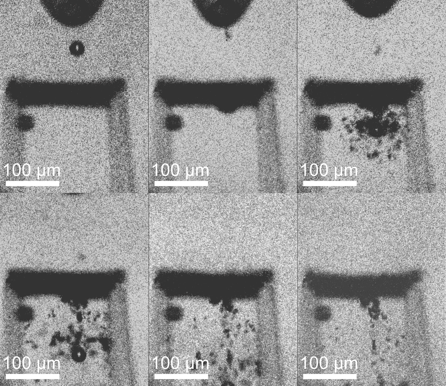
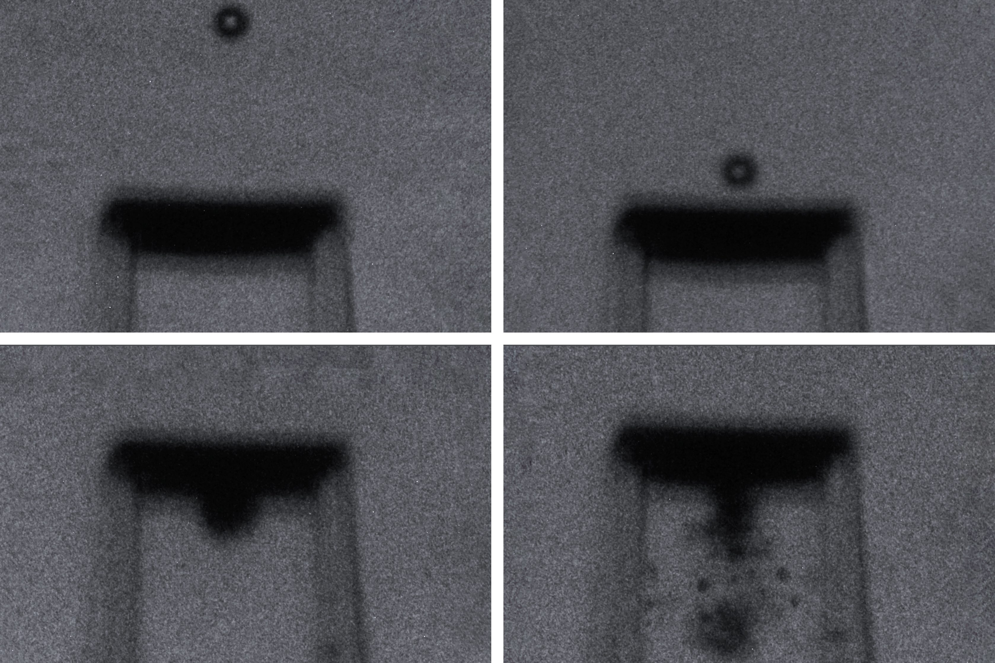
In their experiments, the team suspended tiny printed metamaterial lattices between microscopic support structures, then fired even tinier particles at the materials, at supersonic speeds. With high-speed cameras, the team then captured images of each impact and its aftermath, with nanosecond precision.

Animation of spherical particle smashing through bridge.

Their work has identified a few metamaterial architectures that are more resilient to supersonic impacts compared to their entirely solid, nonarchitected counterparts. The researchers say the results they observed at the microscopic level can be extended to comparable macroscale impacts, to predict how new material structures across length scales will withstand impacts in the real world.

“What we’re learning is, the microstructure of your material matters, even with high-rate deformation,” says study author Carlos Portela, the Brit and Alex d’Arbeloff Career Development Professor in Mechanical Engineering at MIT. “We want to identify impact-resistant structures that can be made into coatings or panels for spacecraft, vehicles, helmets, and anything that needs to be lightweight and protected.”

Other authors on the study include first author and MIT graduate student Thomas Butruille, and Joshua Crone of DEVCOM Army Research Laboratory.

Pure impact

The team’s new high-velocity experiments build off their previous work, in which the engineers tested the resilience of an ultralight, carbon-based material. That material, which was thinner than the width of a human hair, was made from tiny struts and beams of carbon, which the team printed and placed on a glass slide. They then fired microparticles toward the material, at velocities exceeding the speed of sound.  

Those supersonic experiments revealed that the microstructured material withstood the high-velocity impacts, sometimes deflecting the microparticles and other times capturing them.

“But there were many questions we couldn’t answer because we were testing the materials on a substrate, which may have affected their behavior,” Portela says.

In their new study, the researchers developed a way to test freestanding metamaterials, to observe how the materials withstand impacts purely on their own, without a backing or supporting substrate.

In their current setup, the researchers suspend a metamaterial of interest between two microscopic pillars made from the same base material. Depending on the dimensions of the metamaterial being tested, the researchers calculate how far apart the pillars must be in order to support the material at either end while allowing the material to respond to any impacts, without any influence from the pillars themselves.

“This way, we ensure that we’re measuring the material property and not the structural property,” Portela says.

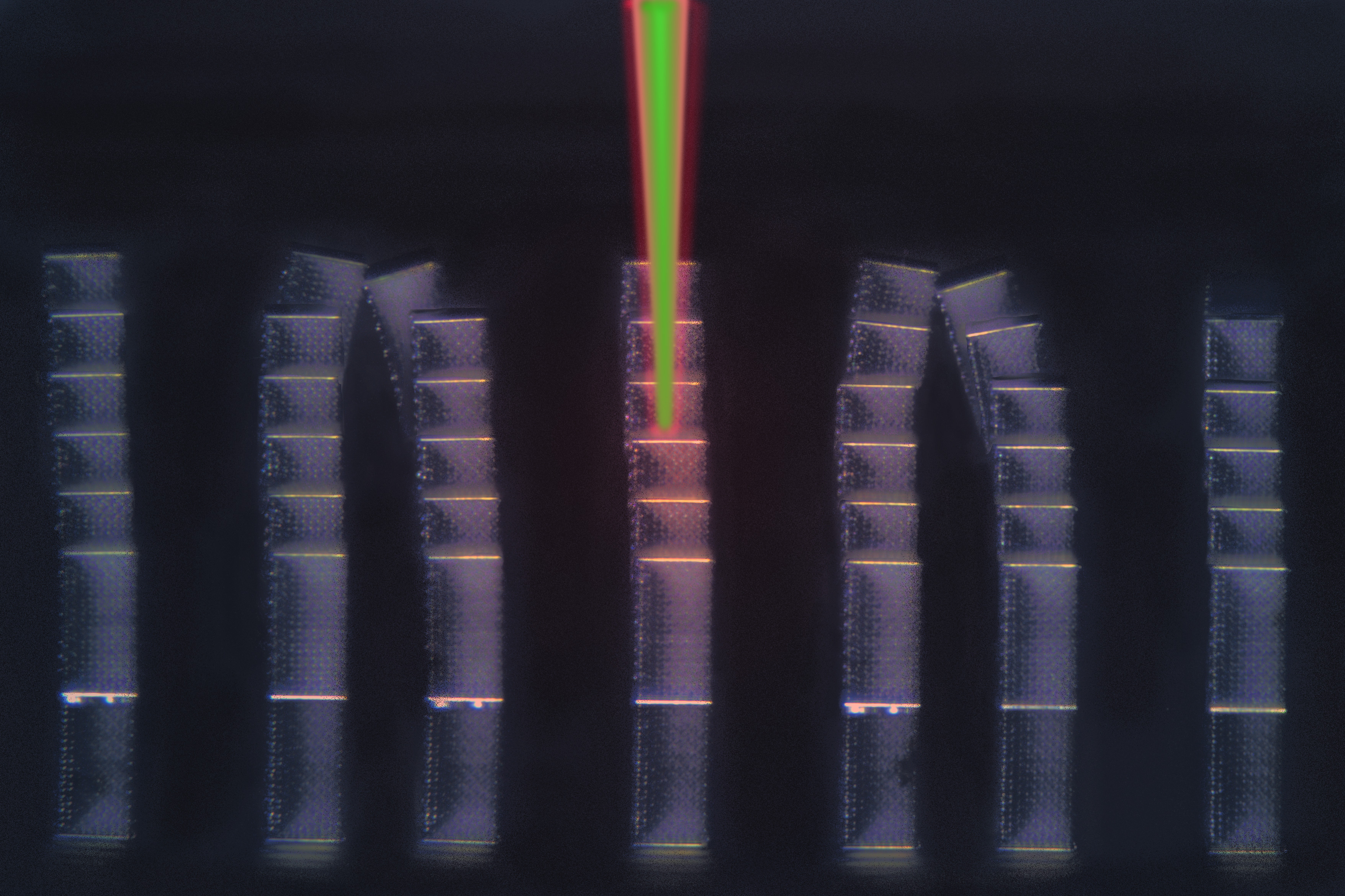
Once the team settled on the pillar support design, they moved on to test a variety of metamaterial architectures. For each architecture, the researchers first printed the supporting pillars on a small silicon chip, then continued printing the metamaterial as a suspended layer between the pillars.

“We can print and test hundreds of these structures on a single chip,” Portela says.

Punctures and cracks

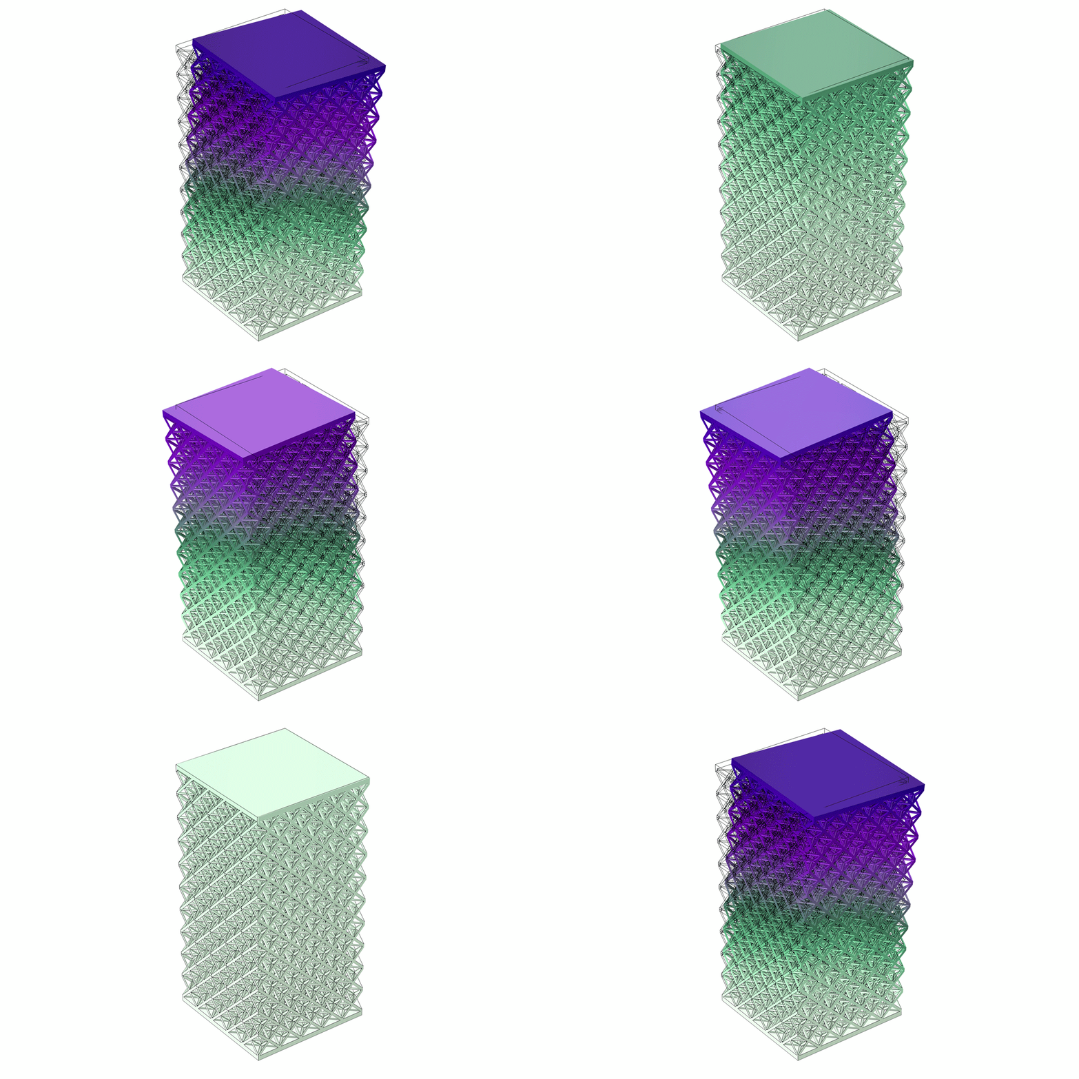
The team printed suspended metamaterials that resembled intricate honeycomb-like cross-sections. Each material was printed with a specific three-dimensional microscopic architecture, such as a precise scaffold of repeating octets, or more faceted polygons. Each repeated unit measured as small as a red blood cell. The resulting metamaterials were thinner than the width of a human hair.

The researchers then tested each metamaterial’s impact resilience by firing glass microparticles toward the structures, at speeds of up to 900 meters per second (more than 2,000 miles per hour) — well within the supersonic range. They caught each impact on camera and studied the resulting images, frame by frame, to see how the projectiles penetrated each material. Next, they examined the materials under a microscope and compared each impact’s physical aftermath.

“In the architected materials, we saw this morphology of small cylindrical craters after impact,” Portela says. “But in solid materials, we saw a lot of radial cracks and bigger chunks of material that were gouged out.”

Overall, the team observed that the fired particles created small punctures in the latticed metamaterials, and the materials nevertheless stayed intact. In contrast, when the same particles were fired at the same speeds into solid, nonlatticed materials of equal mass, they created large cracks that quickly spread, causing the material to crumble. The microstructured materials, therefore, were more efficient in resisting supersonic impacts as well as protecting against multiple impact events. And in particular, materials that were printed with the repeating octets appeared to be the most hardy.

“At the same velocity, we see the octet architecture is harder to fracture, meaning that the metamaterial, per unit mass, can withstand impacts up to twice as much as the bulk material,” Portela says. “This tells us that there are some architectures that can make a material tougher which can offer better impact protection.”

Going forward, the team plans to use the new rapid testing and analysis method to identify new metamaterial designs, in hopes of tagging architectures that can be scaled up to stronger and lighter protective gear, garments, coatings, and paneling.

“What I’m most excited about is showing we can do a lot of these extreme experiments on a benchtop,” Portela says. “This will significantly accelerate the rate at which we can validate new, high-performing, resilient materials.”

This work was funded, in part, by DEVCOM ARL Army Research Office through the MIT Institute for Soldier Nanotechnologies (ISN), and carried out, in part, using ISN’s and MIT.nano’s facilities. 

© Image: Courtesy of the researchers

By firing microparticles at supersonic speeds, MIT engineers can test the resilience of various metamaterials made from structures as small as a red blood cell. Pictured are four video stills of a microparticle hitting a structure made of metamaterials.

Scientists observe record-setting electron mobility in a new crystal film

A material with a high electron mobility is like a highway without traffic. Any electrons that flow into the material experience a commuter’s dream, breezing through without any obstacles or congestion to slow or scatter them off their path.

The higher a material’s electron mobility, the more efficient its electrical conductivity, and the less energy is lost or wasted as electrons zip through. Advanced materials that exhibit high electron mobility will be essential for more efficient and sustainable electronic devices that can do more work with less power.

Now, physicists at MIT, the Army Research Lab, and elsewhere have achieved a record-setting level of electron mobility in a thin film of ternary tetradymite — a class of mineral that is naturally found in deep hydrothermal deposits of gold and quartz.

For this study, the scientists grew pure, ultrathin films of the material, in a way that minimized defects in its crystalline structure. They found that this nearly perfect film — much thinner than a human hair — exhibits the highest electron mobility in its class.

The team was able to estimate the material’s electron mobility by detecting quantum oscillations when electric current passes through. These oscillations are a signature of the quantum mechanical behavior of electrons in a material. The researchers detected a particular rhythm of oscillations that is characteristic of high electron mobility — higher than any ternary thin films of this class to date.

“Before, what people had achieved in terms of electron mobility in these systems was like traffic on a road under construction — you’re backed up, you can’t drive, it’s dusty, and it’s a mess,” says Jagadeesh Moodera, a senior research scientist in MIT’s Department of Physics. “In this newly optimized material, it’s like driving on the Mass Pike with no traffic.”

The team’s results, which appear today in the journal Materials Today Physics, point to ternary tetradymite thin films as a promising material for future electronics, such as wearable thermoelectric devices that efficiently convert waste heat into electricity. (Tetradymites are the active materials that cause the cooling effect in commercial thermoelectric coolers.) The material could also be the basis for spintronic devices, which process information using an electron’s spin, using far less power than conventional silicon-based devices.

The study also uses quantum oscillations as a highly effective tool for measuring a material’s electronic performance.

“We are using this oscillation as a rapid test kit,” says study author Hang Chi, a former research scientist at MIT who is now at the University of Ottawa. “By studying this delicate quantum dance of electrons, scientists can start to understand and identify new materials for the next generation of technologies that will power our world.”

Chi and Moodera’s co-authors include Patrick Taylor, formerly of MIT Lincoln Laboratory, along with Owen Vail and Harry Hier of the Army Research Lab, and Brandi Wooten and Joseph Heremans of Ohio State University.

Beam down

The name “tetradymite” derives from the Greek “tetra” for “four,” and “dymite,” meaning “twin.” Both terms describe the mineral’s crystal structure, which consists of rhombohedral crystals that are “twinned” in groups of four — i.e. they have identical crystal structures that share a side.

Tetradymites comprise combinations of bismuth, antimony tellurium, sulfur, and selenium. In the 1950s, scientists found that tetradymites exhibit semiconducting properties that could be ideal for thermoelectric applications: The mineral in its bulk crystal form was able to passively convert heat into electricity.

Then, in the 1990s, the late Institute Professor Mildred Dresselhaus proposed that the mineral’s thermoelectric properties might be significantly enhanced, not in its bulk form but within its microscopic, nanometer-scale surface, where the interactions of electrons is more pronounced. (Heremans happened to work in Dresselhaus’ group at the time.)

“It became clear that when you look at this material long enough and close enough, new things will happen,” Chi says. “This material was identified as a topological insulator, where scientists could see very interesting phenomena on their surface. But to keep uncovering new things, we have to master the material growth.”

To grow thin films of pure crystal, the researchers employed molecular beam epitaxy — a method by which a beam of molecules is fired at a substrate, typically in a vacuum, and with precisely controlled temperatures. When the molecules deposit on the substrate, they condense and build up slowly, one atomic layer at a time. By controlling the timing and type of molecules deposited, scientists can grow ultrathin crystal films in exact configurations, with few if any defects.

“Normally, bismuth and tellurium can interchange their position, which creates defects in the crystal,” co-author Taylor explains. “The system we used to grow these films came down with me from MIT Lincoln Laboratory, where we use high purity materials to minimize impurities to undetectable limits. It is the perfect tool to explore this research.”

Free flow

The team grew thin films of ternary tetradymite, each about 100 nanometers thin. They then tested the film’s electronic properties by looking for Shubnikov-de Haas quantum oscillations — a phenomenon that was discovered by physicists Lev Shubnikov and Wander de Haas, who found that a material’s electrical conductivity can oscillate when exposed to a strong magnetic field at low temperatures. This effect occurs because the material’s electrons fill up specific energy levels that shift as the magnetic field changes.

Such quantum oscillations could serve as a signature of a material’s electronic structure, and the ways in which electrons behave and interact. Most notably for the MIT team, the oscillations could determine a material’s electron mobility: If oscillations exist, it must mean that the material’s electrical resistance is able to change, and by inference, electrons can be mobile, and made to easily flow.

The team looked for signs of quantum oscillations in their new films, by first exposing them to ultracold temperatures and a strong magnetic field, then running an electric current through the film and measuring the voltage along its path, as they tuned the magnetic field up and down.

“It turns out, to our great joy and excitement, that the material’s electrical resistance oscillates,” Chi says. “Immediately, that tells you that this has very high electron mobility.”

Specifically, the team estimates that the ternary tetradymite thin film exhibits an electron mobility of 10,000 cm2/V-s — the highest mobility of any ternary tetradymite film yet measured. The team suspects that the film’s record mobility has something to do with its low defects and impurities, which they were able to minimize with their precise growth strategies. The fewer a material’s defects, the fewer obstacles an electron encounters, and the more freely it can flow.

“This is showing it’s possible to go a giant step further, when properly controlling these complex systems,” Moodera says. “This tells us we’re in the right direction, and we have the right system to proceed further, to keep perfecting this material down to even much thinner films and proximity coupling for use in future spintronics and wearable thermoelectric devices.”

This research was supported in part by the Army Research Office, National Science Foundation, Office of Naval Research, Canada Research Chairs Program and Natural Sciences and Engineering Research Council of Canada.

© Credit: Courtesy of the researchers; edited by MIT News

Researchers have grown thin films of ternary tetradymite (shown) that exhibit record high electron mobility.

John Joannopoulos receives 2024-2025 Killian Award

John Joannopoulos, an innovator and mentor in the fields of theoretical condensed matter physics and nanophotonics, has been named the recipient of the 2024-2025 James R. Killian Jr. Faculty Achievement Award.

Joannopoulos is the Francis Wright Davis Professor of Physics and director of MIT’s Institute for Soldier Nanotechnologies. He has been a member of the MIT faculty for 50 years.

“Professor Joannopoulos’s profound and lasting impact on the field of theoretical condensed matter physics finds its roots in his pioneering work in harnessing ab initio physics to elucidate the behavior of materials at the atomic level,” states the award citation, which was announced at today’s faculty meeting by Roger White, chair of the Killian Award Selection Committee and professor of philosophy at MIT. “His seminal research in the development of photonic crystals has revolutionized understanding of light-matter interactions, laying the groundwork for transformative advancements in diverse fields ranging from telecommunications to biomedical engineering.”

The award also honors Joannopoulos’ service as a “legendary mentor to generations of students, inspiring them to achieve excellence in science while at the same time facilitating the practical benefit to society through entrepreneurship.”

The Killian Award was established in 1971 to recognize outstanding professional contributions by MIT faculty members. It is the highest honor that the faculty can give to one of its members.

“I have to tell you, it was a complete and utter surprise,” Joannopoulos told MIT News shortly after he received word of the award. “I didn’t expect it at all, and was extremely flattered, honored, and moved by it, frankly.”

Joannopoulous has spent his entire professional career at MIT. He came to the Institute in 1974, directly after receiving his PhD in physics at the University of California at Berkeley, where he also earned his bachelor’s degree. Starting out as an assistant professor in MIT’s Department of Physics, he quickly set up a research program focused on theoretical condensed matter physics.

Over the first half of his MIT career, Joannopoulos worked to elucidate the fundamental nature of the electronic, vibrational, and optical structure of crystalline and amorphous bulk solids, their surfaces, interfaces, and defects. He and his students developed numerous theoretical methods to enable tractable and accurate calculations of these complex systems.

In the 1990s, his work with microscopic material systems expanded to a new class of materials, called photonic crystals — materials that could be engineered at the micro- and nanoscale to manipulate light in ways that impart surprising and exotic optical qualities to the material as a whole.

“I saw that you could create photonic crystals with defects that can affect the properties of photons, in much the same way that defects in a semiconductor affect the properties of electrons,” Joannopoulos says. “So I started working in this area to try and explore what anomalous light phenomena can we discover using this approach?”

Among his various breakthroughs in the field was the realization of a “perfect dielectric mirror” — a multilayered optical device that reflects light from all angles as normal metallic mirrors do, and that can also be tuned to reflect and trap light at specific frequencies. He and his colleagues saw potential for the mirror to be made into a hollow fiber that could serve as a highly effective optical conduit, for use in a wide range of applications. To further advance the technology, he and his colleagues launched a startup, which has since developed the technology into a flexible, fiber-optic “surgical scalpel.”

Throughout his career, Joannopoulos has helped to launch numerous startups and photonics-based technologies.

“His ability to bridge the gap between academia and industry has not only advanced scientific knowledge but also led to the creation of dozens of new companies, thousands of jobs, and groundbreaking products that continue to benefit society to this day,” the award citation states.

In 2006, Joannopoulos accepted the position as director of MIT’s Institute for Soldier Nanotechnologies (ISN), a collaboration between MIT researchers, industry partners, and military defense experts, who seek innovations to protect and enhance soldiers’ survivability in the field. In his role as ISN head, Joannopoulos has worked across MIT, making connections and supporting new projects with researchers specializing in fields far from his own.

“I get a chance to explore and learn fascinating new things,” says Joannopoulos, who is currently overseeing projects related to hyperspectral imaging, smart and responsive fabrics, and nanodrug delivery. “I love that aspect of really getting to understand what people in other fields are doing. And they’re doing great work across many, many different fields.”

Throughout his career at MIT, Joannopoulos has been especially inspired and motivated by his students, many of whom have gone on to found companies, lead top academic and research institutions, and make significant contributions to their respective fields, including one student who was awarded the Nobel Prize in Physics in 1998.

“One’s proudest moments are the successes of one’s students, and in that regard, I’ve been extremely lucky to have had truly exceptional students over the years,” Joannopolous says.

His many contributions to academia and industry have earned Joannopoulos numerous honors and awards, including his election to both the National Academy of Sciences and the American Academy of Arts and Sciences. He is also a fellow of both the American Physical Society and the American Association for the Advancement of Science.

“The Selection Committee is delighted to have this opportunity to honor Professor John Joannopoulos: a visionary scientist, a beloved mentor, a great believer in the goodness of people, and a leader whose contributions to MIT and the broader scientific community are immeasurable,” the award citation concludes.

© Photo: Jose-Luis Olivares, MIT

Physicists arrange atoms in extremely close proximity

Proximity is key for many quantum phenomena, as interactions between atoms are stronger when the particles are close. In many quantum simulators, scientists arrange atoms as close together as possible to explore exotic states of matter and build new quantum materials.

They typically do this by cooling the atoms to a stand-still, then using laser light to position the particles as close as 500 nanometers apart — a limit that is set by the wavelength of light. Now, MIT physicists have developed a technique that allows them to arrange atoms in much closer proximity, down to a mere 50 nanometers. For context, a red blood cell is about 1,000 nanometers wide.

The physicists demonstrated the new approach in experiments with dysprosium, which is the most magnetic atom in nature. They used the new approach to manipulate two layers of dysprosium atoms, and positioned the layers precisely 50 nanometers apart. At this extreme proximity, the magnetic interactions were 1,000 times stronger than if the layers were separated by 500 nanometers.

What’s more, the scientists were able to measure two new effects caused by the atoms’ proximity. Their enhanced magnetic forces caused “thermalization,” or the transfer of heat from one layer to another, as well as synchronized oscillations between layers. These effects petered out as the layers were spaced farther apart.

“We have gone from positioning atoms from 500 nanometers to 50 nanometers apart, and there is a lot you can do with this,” says Wolfgang Ketterle, the John D. MacArthur Professor of Physics at MIT. “At 50 nanometers, the behavior of atoms is so much different that we’re really entering a new regime here.”

Ketterle and his colleagues say the new approach can be applied to many other atoms to study quantum phenomena. For their part, the group plans to use the technique to manipulate atoms into configurations that could generate the first purely magnetic quantum gate — a key building block for a new type of quantum computer.

The team has published their results today in the journal Science. The study’s co-authors include lead author and physics graduate student Li Du, along with Pierre Barral, Michael Cantara, Julius de Hond, and Yu-Kun Lu — all members of the MIT-Harvard Center for Ultracold Atoms, the Department of Physics, and the Research Laboratory of Electronics at MIT.

Peaks and valleys

To manipulate and arrange atoms, physicists typically first cool a cloud of atoms to temperatures approaching absolute zero, then use a system of laser beams to corral the atoms into an optical trap.

Laser light is an electromagnetic wave with a specific wavelength (the distance between maxima of the electric field) and frequency. The wavelength limits the smallest pattern into which light can be shaped to typically 500 nanometers, the so-called optical resolution limit. Since atoms are attracted by laser light of certain frequencies, atoms will be positioned at the points of peak laser intensity. For this reason, existing techniques have been limited in how close they can position atomic particles, and could not be used to explore phenomena that happen at much shorter distances.

“Conventional techniques stop at 500 nanometers, limited not by the atoms but by the wavelength of light,” Ketterle explains. “We have found now a new trick with light where we can break through that limit.”

The team’s new approach, like current techniques, starts by cooling a cloud of atoms — in this case, to about 1 microkelvin, just a hair above absolute zero — at which point, the atoms come to a near-standstill. Physicists can then use lasers to move the frozen particles into desired configurations.

Then, Du and his collaborators worked with two laser beams, each with a different frequency, or color, and circular polarization, or direction of the laser’s electric field. When the two beams travel through a super-cooled cloud of atoms, the atoms can orient their spin in opposite directions, following either of the two lasers’ polarization. The result is that the beams produce two groups of the same atoms, only with opposite spins.

Each laser beam formed a standing wave, a periodic pattern of electric field intensity with a spatial period of 500 nanometers. Due to their different polarizations, each standing wave attracted and corralled one of two groups of atoms, depending on their spin. The lasers could be overlaid and tuned such that the distance between their respective peaks is as small as 50 nanometers, meaning that the atoms gravitating to each respective laser’s peaks would be separated by the same 50 nanometers.

But in order for this to happen, the lasers would have to be extremely stable and immune to all external noise, such as from shaking or even breathing on the experiment. The team realized they could stabilize both lasers by directing them through an optical fiber, which served to lock the light beams in place in relation to each other.

“The idea of sending both beams through the optical fiber meant the whole machine could shake violently, but the two laser beams stayed absolutely stable with respect to each others,” Du says.

Magnetic forces at close range

As a first test of their new technique, the team used atoms of dysprosium — a rare-earth metal that is one of the strongest magnetic elements in the periodic table, particularly at ultracold temperatures. However, at the scale of atoms, the element’s magnetic interactions are relatively weak at distances of even 500 nanometers. As with common refrigerator magnets, the magnetic attraction between atoms increases with proximity, and the scientists suspected that if their new technique could space dysprosium atoms as close as 50 nanometers apart, they might observe the emergence of otherwise weak interactions between the magnetic atoms.

“We could suddenly have magnetic interactions, which used to be almost neglible but now are really strong,” Ketterle says.

The team applied their technique to dysprosium, first super-cooling the atoms, then passing two lasers through to split the atoms into two spin groups, or layers. They then directed the lasers through an optical fiber to stabilize them, and found that indeed, the two layers of dysprosium atoms gravitated to their respective laser peaks, which in effect separated the layers of atoms by 50 nanometers — the closest distance that any ultracold atom experiment has been able to achieve.

At this extremely close proximity, the atoms’ natural magnetic interactions were significantly enhanced, and were 1,000 times stronger than if they were positioned 500 nanometers apart. The team observed that these interactions resulted in two novel quantum phenomena: collective oscillation, in which one layer’s vibrations caused the other layer to vibrate in sync; and thermalization, in which one layer transferred heat to the other, purely through magnetic fluctuations in the atoms.

“Until now, heat between atoms could only by exchanged when they were in the same physical space and could collide,” Du notes. “Now we have seen atomic layers, separated by vacuum, and they exchange heat via fluctuating magnetic fields.”

The team’s results introduce a new technique that can be used to position many types of atom in close proximity. They also show that atoms, placed close enough together, can exhibit interesting quantum phenomena, that could be harnessed to build new quantum materials, and potentially, magnetically-driven atomic systems for quantum computers.

“We are really bringing super-resolution methods to the field, and it will become a general tool for doing quantum simulations,” Ketterle says. “There are many variants possible, which we are working on.”

This research was funded, in part, by the National Science Foundation and the Department of Defense.

© Image: Courtesy of the researchers; MIT News

MIT physicists developed a technique to arrange atoms (represented as spheres with arrows) in much closer proximity than previously possible, down to 50 nanometers. The group plans to use the method to manipulate atoms into configurations that could generate the first purely magnetic quantum gate — a key building block for a new type of quantum computer. In this image, the magnetic interaction is represented by the colorful lines.

“Nanostitches” enable lighter and tougher composite materials

To save on fuel and reduce aircraft emissions, engineers are looking to build lighter, stronger airplanes out of advanced composites. These engineered materials are made from high-performance fibers that are embedded in polymer sheets. The sheets can be stacked and pressed into one multilayered material and made into extremely lightweight and durable structures.

But composite materials have one main vulnerability: the space between layers, which is typically filled with polymer “glue” to bond the layers together. In the event of an impact or strike, cracks can easily spread between layers and weaken the material, even though there may be no visible damage to the layers themselves. Over time, as these hidden cracks spread between layers, the composite could suddenly crumble without warning.

Now, MIT engineers have shown they can prevent cracks from spreading between composite’s layers, using an approach they developed called “nanostitching,” in which they deposit chemically grown microscopic forests of carbon nanotubes between composite layers. The tiny, densely packed fibers grip and hold the layers together, like ultrastrong Velcro, preventing the layers from peeling or shearing apart.

In experiments with an advanced composite known as thin-ply carbon fiber laminate, the team demonstrated that layers bonded with nanostitching improved the material’s resistance to cracks by up to 60 percent, compared with composites with conventional polymers. The researchers say the results help to address the main vulnerability in advanced composites.

“Just like phyllo dough flakes apart, composite layers can peel apart because this interlaminar region is the Achilles’ heel of composites,” says Brian Wardle, professor of aeronautics and astronautics at MIT. “We’re showing that nanostitching makes this normally weak region so strong and tough that a crack will not grow there. So, we could expect the next generation of aircraft to have composites held together with this nano-Velcro, to make aircraft safer and have greater longevity.”

Wardle and his colleagues have published their results today in the journal ACS Applied Materials and Interfaces. The study’s first author is former MIT visiting graduate student and postdoc Carolina Furtado, along with Reed Kopp, Xinchen Ni, Carlos Sarrado, Estelle Kalfon-Cohen, and Pedro Camanho.

Forest growth

At MIT, Wardle is director of the necstlab (pronounced “next lab”), where he and his group first developed the concept for nanostitching. The approach involves “growing” a forest of vertically aligned carbon nanotubes — hollow fibers of carbon, each so small that tens of billions of the the nanotubes can stand in an area smaller than a fingernail. To grow the nanotubes, the team used a process of chemical vapor deposition to react various catalysts in an oven, causing carbon to settle onto a surface as tiny, hair-like supports. The supports are eventually removed, leaving behind a densely packed forest of microscopic, vertical rolls of carbon.

The lab has previously shown that the nanotube forests can be grown and adhered to layers of composite material, and that this fiber-reinforced compound improves the material’s overall strength. The researchers had also seen some signs that the fibers can improve a composite’s resistance to cracks between layers.

In their new study, the engineers took a more in-depth look at the between-layer region in composites to test and quantify how nanostitching would improve the region’s resistance to cracks. In particular, the study focused on an advanced composite material known as thin-ply carbon fiber laminates.

“This is an emerging composite technology, where each layer, or ply, is about 50 microns thin, compared to standard composite plies that are 150 microns, which is about the diameter of a human hair. There’s evidence to suggest they are better than standard-thickness composites. And we wanted to see whether there might be synergy between our nanostitching and this thin-ply technology, since it could lead to more resilient aircraft, high-value aerospace structures, and space and military vehicles,” Wardle says.

Velcro grip

The study’s experiments were led by Carolina Furtado, who joined the effort as part of the MIT-Portugal program in 2016, continued the project as a postdoc, and is now a professor at the University of Porto in Portugal, where her research focuses on modeling cracks and damage in advanced composites.

In her tests, Furtado used the group’s techniques of chemical vapor deposition to grow densely packed forests of vertically aligned carbon nanotubes. She also fabricated samples of thin-ply carbon fiber laminates. The resulting advanced composite was about 3 millimeters thick and comprised 60 layers, each made from stiff, horizontal fibers embedded in a polymer sheet.

She transferred and adhered the nanotube forest in between the two middle layers of the composite, then cooked the material in an autoclave to cure. To test crack resistance, the researchers placed a crack on the edge of the composite, right at the start of the region between the two middle layers.

“In fracture testing, we always start with a crack because we want to test whether and how far the crack will spread,” Furtado explains.

The researchers then placed samples of the nanotube-reinforced composite in an experimental setup to test their resilience to “delamination,” or the potential for layers to separate.

“There’s lots of ways you can get precursors to delamination, such as from impacts, like tool drop, bird strike, runway kickup in aircraft, and there could be almost no visible damage, but internally it has a delamination,” Wardle says. “Just like a human, if you’ve got a hairline fracture in a bone, it’s not good. Just because you can’t see it doesn’t mean it’s not impacting you. And damage in composites is hard to inspect.”

To examine nanostitching’s potential to prevent delamination, the team placed their samples in a setup to test three delamination modes, in which a crack could spread through the between-layer region and peel the layers apart or cause them to slide against each other, or do a combination of both. All three of these modes are the most common ways in which conventional composites can internally flake and crumble.

The tests, in which the researchers precisely measured the force required to peel or shear the composite’s layers, revealed that the nanostitched held fast, and the initial crack that the researchers made was unable to spread further between the layers. The nanostitched samples were up to 62 percent tougher and more resistant to cracks, compared with the same advanced composite material that was held together with conventional polymers.

“This is a new composite technology, turbocharged by our nanotubes,” Wardle says.

“The authors have demonsrated that thin plies and nanostitching together have made significant increase in toughness,” says Stephen Tsai, emeritus professor of aeronautics and astronautics at Stanford University. “Composites are degraded by their weak interlaminar strength. Any improvement shown in this work will increase the design allowable, and reduce the weight and cost of composites technology.”

The researchers envision that any vehicle or structure that incorporates conventional composites could be made lighter, tougher, and more resilient with nanostitching.

“You could have selective reinforcement of problematic areas, to reinforce holes or bolted joints, or places where delamination might happen,” Furtado says. “This opens a big window of opportunity.”

© Image: Courtesy of the researchers, edited by MIT News

This schematic shows an engineered material with composite layers. Layers of carbon fibers (the long silver tubes) have microscopic forests of carbon nanotubes between them (the array of tiny brown objects). These tiny, densely packed fibers grip and hold the layers together, like ultrastrong Velcro, preventing the layers from peeling or shearing apart.

Pushing material boundaries for better electronics

Undergrads, take note: The lessons you learn in those intro classes could be the key to making your next big discovery. At least, that’s been the case for MIT’s Jeehwan Kim.

A recently tenured faculty member in MIT’s departments of Mechanical Engineering and Materials Science and Engineering, Kim has made numerous discoveries about the nanostructure of materials and is funneling them directly into the advancement of next-generation electronics.

His research aims to push electronics past the inherent limits of silicon — a material that has reliably powered transistors and most other electronic elements but is reaching a performance limit as more computing power is packed into ever smaller devices.

Today, Kim and his students at MIT are exploring materials, devices, and systems that could take over where silicon leaves off. Kim is applying his insights to design next-generation devices, including low-power, high-performance transistors and memory devices, artificial intelligence chips, ultra-high-definition micro-LED displays, and flexible electronic “skin.” Ultimately, he envisions such beyond-silicon devices could be built into supercomputers small enough to fit in your pocket.

The innovations that have come out of his research are recorded in more than 200 issued U.S. patents and 70 research papers — an extensive list that he and his students continue to grow.

Kim credits many of his breakthroughs to the fundamentals he learned in his university days. In fact, he has carried his college textbooks and notes with him with every move. Today, he keeps the undergraduate notes — written in a light and meticulous graphite and ink — on a shelf nearest to his MIT desk, close at hand. He references them in his own class lectures and presentations, and when brainstorming research solutions.

“These textbooks are all in my brain now,” Kim says. “I’ve learned that if you completely understand the fundamentals, you can solve any problem.”

Fundamental shift

Kim wasn’t always a model student. Growing up in Seoul, South Korea, he was fixed on a musical career. He had a passion for singing and was bored by most other high school subjects.

“It was very monotonic,” Kim recalls. “My motivation for high school subjects was very low.”

After graduating high school, he enrolled in a materials science program at Hongik University, where he was lucky to met professors who had graduated from MIT and who later motivated him to study in the United States. But, Kim spent his first year there trying to make it as a musician. He wrote and sang songs that he recorded and sent to promoters, and went to multiple auditions. But after a year, he was faced with no call-backs, and a hard question.

“What should I do? It was a crisis to me,” Kim says.

In his second year, he decided to give materials science a go. When he sat in on his first class, he was surprised to find that the subject — the structure and behavior of materials at the atomic scale — made him want to learn more.

“My first year, my GPA was almost zero because I didn’t attend class, and was going to be kicked out,” Kim says. “Then from my second year on, I really loved every single subject in materials science. People who saw me in the library were surprised: ‘What are you doing here, without a guitar?’ I must have read these textbooks more than 10 times, and felt I really understood everything fundamental.”

Back to basics

He took this newfound passion to Seoul National University, where he enrolled in the materials science master’s program and learned to apply the ideas he absorbed to hands-on research problems. Metallurgy was a dominant field at the time, and Kim was assigned to experiment with high-temperature alloys — mixing and melting metallic powders to create materials that could be used in high-performance engines.

After completing his master’s, Kim wanted to continue with a PhD, overseas. But to do so, he first had to serve in the military. He spent the next two and a half years in the Korean air force, helping to maintain and refuel aircraft, and inventory their parts. All the while, he prepared applications to graduate schools abroad.

In 2003, after completing his service, he headed overseas, where he was accepted to the materials science graduate program at the University of California at Los Angeles with a fellowship.

“When I came out of the airplane and went to the dorm for the first day, people were drinking Corona on the balcony, playing music, and there was beautiful weather, and I thought, this is where I’m supposed to be!” Kim recalls.

For his PhD, he began to dive into the microscopic world of electronic materials, seeking ways to manipulate them to make faster electronics. The subject was a focus for his advisor, who previously worked at Bell Labs, where many computing innovations originated at the time.

“A lot of the papers I was reading were from Bell Labs, and IBM T.J. Watson, and I was so impressed, and thought: I really want to be a scientist there. That was my dream,” Kim says.

During his PhD program, he reached out to a scientist at IBM whose name kept coming up in the papers Kim was reading. In his initial letter, Kim wrote with a question about his own PhD work, which tackled a hard industry problem: how to stretch, or “strain,” silicon to minimize defects that would occur as more transistors are packed on a chip. 

The query opened a dialogue, and Kim eventually inquired and was accepted to an internship at the IBM T.J. Watson Research Center, just outside New York City. Soon after he arrived, his manager pitched him a challenge: He might be hired full-time if he could solve a new, harder problem, having to do with replacing silicon.

At the time, the electronics industry was looking to germanium as a possible successor to silicon. The material can conduct electrons at even smaller scales, which would enable germanium to be made into even tinier transistors, for faster, smaller, and more powerful devices. But there was no reliable way for germanium to be “doped” — an essential process that replaces some of a material’s atoms with another type of atom in a way that controls how electrons flow through the material.

“My manager told me he didn’t expect me to solve this. But I really wanted the job,” Kim says. “So day and night, I thought, how to solve this? And I always went back to the textbooks.”

Those textbooks reminded him of a fundamental rule: Replacing one atom with another would work well if both atoms were of similar size. This revelation triggered an idea. Perhaps germanium could be doped with a combination of two different atoms with an average atomic size that is similar to germanium’s.

“I came up with this idea, and right after, IBM showed that it worked. I was so amazed,” Kim says. “From that point, research became my passion. I did it because it was just so fun. Singing is not so different from performing research.”

As promised, he was hired as a postdoc and soon after, promoted to research staff member — a title he carried, literally, with pride.

“I was feeling so happy to be there,” Kim says. “I even wore my IBM badge to restaurants, and everywhere I went.”

Throughout his time at IBM, he learned to focus on research that directly impacts everyday human life, and how to apply the fundamentals to develop next-generation products.

“IBM really raised me up as an engineer who can identify the problems in an industry and find creative solutions to tackle the challenges,” he says.

Cycle of life

And yet, Kim felt he could do more. He was working on boundary-pushing research at one of the leading innovation hubs in the country, where “out-of-the-box” thinking was encouraged, and experimentally tested. But he wanted to explore beyond the company’s research portfolio, and also, find a way to pursue research not just as a profession but as a passion.

“My experience taught me that you can lead a very happy life as an engineer or scientist if your research becomes your hobby,” Kim says. “I wanted to teach this cycle — of happiness, research, and passion — to young people and help PhD students develop like artists or singers.”

In 2015, he packed his bags for MIT, where he accepted a junior faculty position in the Department of Mechanical Engineering. His first impressions upon arriving at the Institute?

“Freedom,” Kim says. “For me, free thinking — to compose music, innovate something totally new — is the most important thing. And the people at MIT are very talented and curious of all the things.”

Since he’s put down roots on campus, he has built up a highly productive research group, focused on fabricating ultra-thin, stackable, high-performance electronic materials and devices, which Kim envisions could be used to build hybrid electronic systems as small as a fingernail and as powerful as a supercomputer. He credits the group’s many innovations to the more than 40 students, postdocs, and research scientists who have contributed to his lab.

“I hope this is where they can learn that research can be an art,” Kim says. “To students especially, I hope they see that, if they enjoy what they do, then they can be whatever they want to be.”

© Photo: Jake Belcher

“For me, free thinking — to compose music, innovate something totally new — is the most important thing. And the people at MIT are very talented and curious of all the things,” says Jeehwan Kim.

Benchtop test quickly identifies extremely impact-resistant materials

An intricate, honeycomb-like structure of struts and beams could withstand a supersonic impact better than a solid slab of the same material. What’s more, the specific structure matters, with some being more resilient to impacts than others.

That’s what MIT engineers are finding in experiments with microscopic metamaterials — materials that are intentionally printed, assembled, or otherwise engineered with microscopic architectures that give the overall material exceptional properties.

In a study appearing today in the Proceedings of the National Academy of Sciences, the engineers report on a new way to quickly test an array of metamaterial architectures and their resilience to supersonic impacts.

In their experiments, the team suspended tiny printed metamaterial lattices between microscopic support structures, then fired even tinier particles at the materials, at supersonic speeds. With high-speed cameras, the team then captured images of each impact and its aftermath, with nanosecond precision.

Animation of spherical particle smashing through bridge.

Their work has identified a few metamaterial architectures that are more resilient to supersonic impacts compared to their entirely solid, nonarchitected counterparts. The researchers say the results they observed at the microscopic level can be extended to comparable macroscale impacts, to predict how new material structures across length scales will withstand impacts in the real world.

“What we’re learning is, the microstructure of your material matters, even with high-rate deformation,” says study author Carlos Portela, the Brit and Alex d’Arbeloff Career Development Professor in Mechanical Engineering at MIT. “We want to identify impact-resistant structures that can be made into coatings or panels for spacecraft, vehicles, helmets, and anything that needs to be lightweight and protected.”

Other authors on the study include first author and MIT graduate student Thomas Butruille, and Joshua Crone of DEVCOM Army Research Laboratory.

Pure impact

The team’s new high-velocity experiments build off their previous work, in which the engineers tested the resilience of an ultralight, carbon-based material. That material, which was thinner than the width of a human hair, was made from tiny struts and beams of carbon, which the team printed and placed on a glass slide. They then fired microparticles toward the material, at velocities exceeding the speed of sound.  

Those supersonic experiments revealed that the microstructured material withstood the high-velocity impacts, sometimes deflecting the microparticles and other times capturing them.

“But there were many questions we couldn’t answer because we were testing the materials on a substrate, which may have affected their behavior,” Portela says.

In their new study, the researchers developed a way to test freestanding metamaterials, to observe how the materials withstand impacts purely on their own, without a backing or supporting substrate.

In their current setup, the researchers suspend a metamaterial of interest between two microscopic pillars made from the same base material. Depending on the dimensions of the metamaterial being tested, the researchers calculate how far apart the pillars must be in order to support the material at either end while allowing the material to respond to any impacts, without any influence from the pillars themselves.

“This way, we ensure that we’re measuring the material property and not the structural property,” Portela says.

Once the team settled on the pillar support design, they moved on to test a variety of metamaterial architectures. For each architecture, the researchers first printed the supporting pillars on a small silicon chip, then continued printing the metamaterial as a suspended layer between the pillars.

“We can print and test hundreds of these structures on a single chip,” Portela says.

Punctures and cracks

The team printed suspended metamaterials that resembled intricate honeycomb-like cross-sections. Each material was printed with a specific three-dimensional microscopic architecture, such as a precise scaffold of repeating octets, or more faceted polygons. Each repeated unit measured as small as a red blood cell. The resulting metamaterials were thinner than the width of a human hair.

The researchers then tested each metamaterial’s impact resilience by firing glass microparticles toward the structures, at speeds of up to 900 meters per second (more than 2,000 miles per hour) — well within the supersonic range. They caught each impact on camera and studied the resulting images, frame by frame, to see how the projectiles penetrated each material. Next, they examined the materials under a microscope and compared each impact’s physical aftermath.

“In the architected materials, we saw this morphology of small cylindrical craters after impact,” Portela says. “But in solid materials, we saw a lot of radial cracks and bigger chunks of material that were gouged out.”

Overall, the team observed that the fired particles created small punctures in the latticed metamaterials, and the materials nevertheless stayed intact. In contrast, when the same particles were fired at the same speeds into solid, nonlatticed materials of equal mass, they created large cracks that quickly spread, causing the material to crumble. The microstructured materials, therefore, were more efficient in resisting supersonic impacts as well as protecting against multiple impact events. And in particular, materials that were printed with the repeating octets appeared to be the most hardy.

“At the same velocity, we see the octet architecture is harder to fracture, meaning that the metamaterial, per unit mass, can withstand impacts up to twice as much as the bulk material,” Portela says. “This tells us that there are some architectures that can make a material tougher which can offer better impact protection.”

Going forward, the team plans to use the new rapid testing and analysis method to identify new metamaterial designs, in hopes of tagging architectures that can be scaled up to stronger and lighter protective gear, garments, coatings, and paneling.

“What I’m most excited about is showing we can do a lot of these extreme experiments on a benchtop,” Portela says. “This will significantly accelerate the rate at which we can validate new, high-performing, resilient materials.”

This work was funded, in part, by DEVCOM ARL Army Research Office through the MIT Institute for Soldier Nanotechnologies (ISN), and carried out, in part, using ISN’s and MIT.nano’s facilities. 

© Image: Courtesy of the researchers

By firing microparticles at supersonic speeds, MIT engineers can test the resilience of various metamaterials made from structures as small as a red blood cell. Pictured are four video stills of a microparticle hitting a structure made of metamaterials.

Scientists observe record-setting electron mobility in a new crystal film

A material with a high electron mobility is like a highway without traffic. Any electrons that flow into the material experience a commuter’s dream, breezing through without any obstacles or congestion to slow or scatter them off their path.

The higher a material’s electron mobility, the more efficient its electrical conductivity, and the less energy is lost or wasted as electrons zip through. Advanced materials that exhibit high electron mobility will be essential for more efficient and sustainable electronic devices that can do more work with less power.

Now, physicists at MIT, the Army Research Lab, and elsewhere have achieved a record-setting level of electron mobility in a thin film of ternary tetradymite — a class of mineral that is naturally found in deep hydrothermal deposits of gold and quartz.

For this study, the scientists grew pure, ultrathin films of the material, in a way that minimized defects in its crystalline structure. They found that this nearly perfect film — much thinner than a human hair — exhibits the highest electron mobility in its class.

The team was able to estimate the material’s electron mobility by detecting quantum oscillations when electric current passes through. These oscillations are a signature of the quantum mechanical behavior of electrons in a material. The researchers detected a particular rhythm of oscillations that is characteristic of high electron mobility — higher than any ternary thin films of this class to date.

“Before, what people had achieved in terms of electron mobility in these systems was like traffic on a road under construction — you’re backed up, you can’t drive, it’s dusty, and it’s a mess,” says Jagadeesh Moodera, a senior research scientist in MIT’s Department of Physics. “In this newly optimized material, it’s like driving on the Mass Pike with no traffic.”

The team’s results, which appear today in the journal Materials Today Physics, point to ternary tetradymite thin films as a promising material for future electronics, such as wearable thermoelectric devices that efficiently convert waste heat into electricity. (Tetradymites are the active materials that cause the cooling effect in commercial thermoelectric coolers.) The material could also be the basis for spintronic devices, which process information using an electron’s spin, using far less power than conventional silicon-based devices.

The study also uses quantum oscillations as a highly effective tool for measuring a material’s electronic performance.

“We are using this oscillation as a rapid test kit,” says study author Hang Chi, a former research scientist at MIT who is now at the University of Ottawa. “By studying this delicate quantum dance of electrons, scientists can start to understand and identify new materials for the next generation of technologies that will power our world.”

Chi and Moodera’s co-authors include Patrick Taylor, formerly of MIT Lincoln Laboratory, along with Owen Vail and Harry Hier of the Army Research Lab, and Brandi Wooten and Joseph Heremans of Ohio State University.

Beam down

The name “tetradymite” derives from the Greek “tetra” for “four,” and “dymite,” meaning “twin.” Both terms describe the mineral’s crystal structure, which consists of rhombohedral crystals that are “twinned” in groups of four — i.e. they have identical crystal structures that share a side.

Tetradymites comprise combinations of bismuth, antimony tellurium, sulfur, and selenium. In the 1950s, scientists found that tetradymites exhibit semiconducting properties that could be ideal for thermoelectric applications: The mineral in its bulk crystal form was able to passively convert heat into electricity.

Then, in the 1990s, the late Institute Professor Mildred Dresselhaus proposed that the mineral’s thermoelectric properties might be significantly enhanced, not in its bulk form but within its microscopic, nanometer-scale surface, where the interactions of electrons is more pronounced. (Heremans happened to work in Dresselhaus’ group at the time.)

“It became clear that when you look at this material long enough and close enough, new things will happen,” Chi says. “This material was identified as a topological insulator, where scientists could see very interesting phenomena on their surface. But to keep uncovering new things, we have to master the material growth.”

To grow thin films of pure crystal, the researchers employed molecular beam epitaxy — a method by which a beam of molecules is fired at a substrate, typically in a vacuum, and with precisely controlled temperatures. When the molecules deposit on the substrate, they condense and build up slowly, one atomic layer at a time. By controlling the timing and type of molecules deposited, scientists can grow ultrathin crystal films in exact configurations, with few if any defects.

“Normally, bismuth and tellurium can interchange their position, which creates defects in the crystal,” co-author Taylor explains. “The system we used to grow these films came down with me from MIT Lincoln Laboratory, where we use high purity materials to minimize impurities to undetectable limits. It is the perfect tool to explore this research.”

Free flow

The team grew thin films of ternary tetradymite, each about 100 nanometers thin. They then tested the film’s electronic properties by looking for Shubnikov-de Haas quantum oscillations — a phenomenon that was discovered by physicists Lev Shubnikov and Wander de Haas, who found that a material’s electrical conductivity can oscillate when exposed to a strong magnetic field at low temperatures. This effect occurs because the material’s electrons fill up specific energy levels that shift as the magnetic field changes.

Such quantum oscillations could serve as a signature of a material’s electronic structure, and the ways in which electrons behave and interact. Most notably for the MIT team, the oscillations could determine a material’s electron mobility: If oscillations exist, it must mean that the material’s electrical resistance is able to change, and by inference, electrons can be mobile, and made to easily flow.

The team looked for signs of quantum oscillations in their new films, by first exposing them to ultracold temperatures and a strong magnetic field, then running an electric current through the film and measuring the voltage along its path, as they tuned the magnetic field up and down.

“It turns out, to our great joy and excitement, that the material’s electrical resistance oscillates,” Chi says. “Immediately, that tells you that this has very high electron mobility.”

Specifically, the team estimates that the ternary tetradymite thin film exhibits an electron mobility of 10,000 cm2/V-s — the highest mobility of any ternary tetradymite film yet measured. The team suspects that the film’s record mobility has something to do with its low defects and impurities, which they were able to minimize with their precise growth strategies. The fewer a material’s defects, the fewer obstacles an electron encounters, and the more freely it can flow.

“This is showing it’s possible to go a giant step further, when properly controlling these complex systems,” Moodera says. “This tells us we’re in the right direction, and we have the right system to proceed further, to keep perfecting this material down to even much thinner films and proximity coupling for use in future spintronics and wearable thermoelectric devices.”

This research was supported in part by the Army Research Office, National Science Foundation, Office of Naval Research, Canada Research Chairs Program and Natural Sciences and Engineering Research Council of Canada.

© Credit: Courtesy of the researchers; edited by MIT News
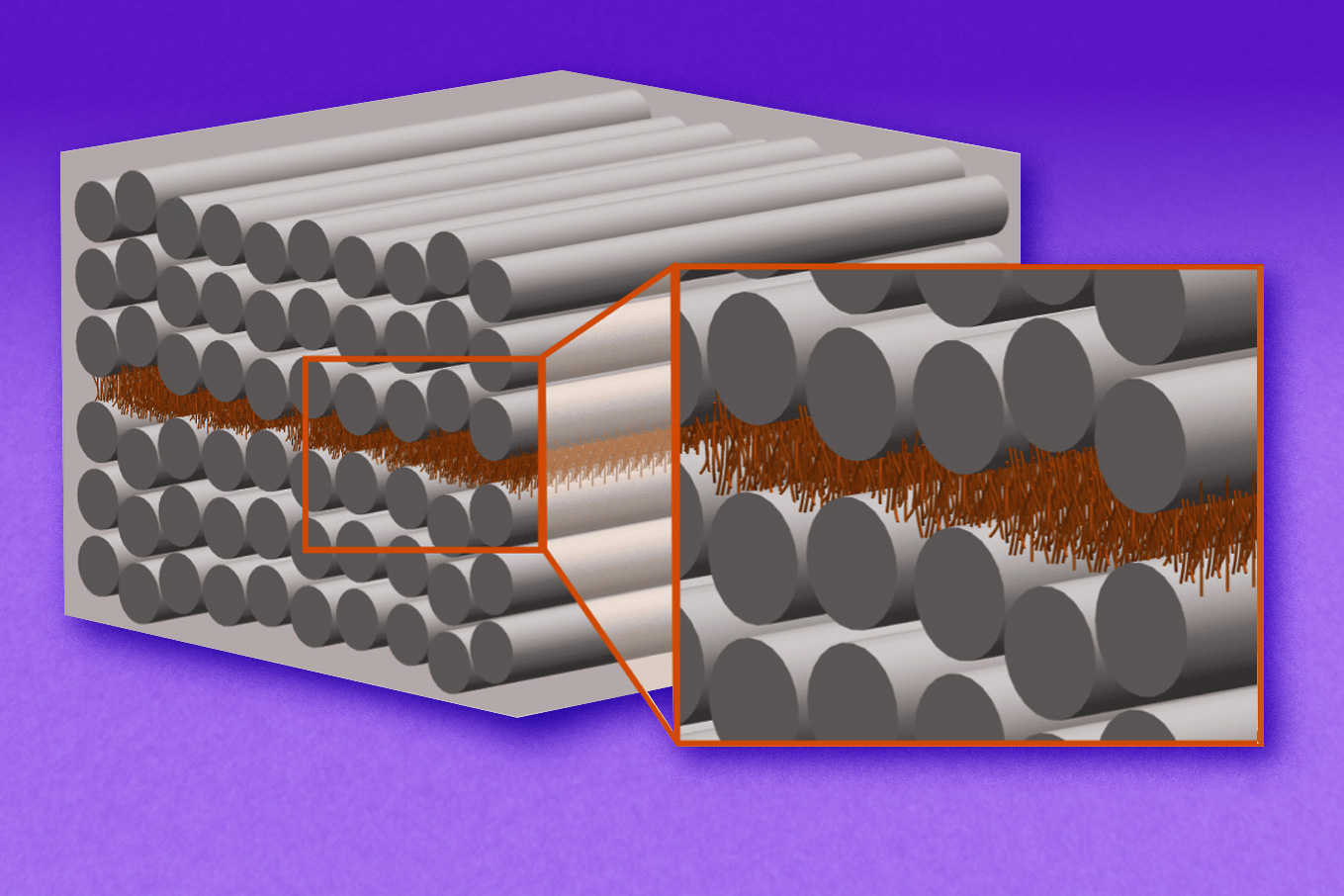
Researchers have grown thin films of ternary tetradymite (shown) that exhibit record high electron mobility.

John Joannopoulos receives 2024-2025 Killian Award

John Joannopoulos, an innovator and mentor in the fields of theoretical condensed matter physics and nanophotonics, has been named the recipient of the 2024-2025 James R. Killian Jr. Faculty Achievement Award.

Joannopoulos is the Francis Wright Davis Professor of Physics and director of MIT’s Institute for Soldier Nanotechnologies. He has been a member of the MIT faculty for 50 years.

“Professor Joannopoulos’s profound and lasting impact on the field of theoretical condensed matter physics finds its roots in his pioneering work in harnessing ab initio physics to elucidate the behavior of materials at the atomic level,” states the award citation, which was announced at today’s faculty meeting by Roger White, chair of the Killian Award Selection Committee and professor of philosophy at MIT. “His seminal research in the development of photonic crystals has revolutionized understanding of light-matter interactions, laying the groundwork for transformative advancements in diverse fields ranging from telecommunications to biomedical engineering.”

The award also honors Joannopoulos’ service as a “legendary mentor to generations of students, inspiring them to achieve excellence in science while at the same time facilitating the practical benefit to society through entrepreneurship.”

The Killian Award was established in 1971 to recognize outstanding professional contributions by MIT faculty members. It is the highest honor that the faculty can give to one of its members.

“I have to tell you, it was a complete and utter surprise,” Joannopoulos told MIT News shortly after he received word of the award. “I didn’t expect it at all, and was extremely flattered, honored, and moved by it, frankly.”

Joannopoulous has spent his entire professional career at MIT. He came to the Institute in 1974, directly after receiving his PhD in physics at the University of California at Berkeley, where he also earned his bachelor’s degree. Starting out as an assistant professor in MIT’s Department of Physics, he quickly set up a research program focused on theoretical condensed matter physics.

Over the first half of his MIT career, Joannopoulos worked to elucidate the fundamental nature of the electronic, vibrational, and optical structure of crystalline and amorphous bulk solids, their surfaces, interfaces, and defects. He and his students developed numerous theoretical methods to enable tractable and accurate calculations of these complex systems.

In the 1990s, his work with microscopic material systems expanded to a new class of materials, called photonic crystals — materials that could be engineered at the micro- and nanoscale to manipulate light in ways that impart surprising and exotic optical qualities to the material as a whole.

“I saw that you could create photonic crystals with defects that can affect the properties of photons, in much the same way that defects in a semiconductor affect the properties of electrons,” Joannopoulos says. “So I started working in this area to try and explore what anomalous light phenomena can we discover using this approach?”

Among his various breakthroughs in the field was the realization of a “perfect dielectric mirror” — a multilayered optical device that reflects light from all angles as normal metallic mirrors do, and that can also be tuned to reflect and trap light at specific frequencies. He and his colleagues saw potential for the mirror to be made into a hollow fiber that could serve as a highly effective optical conduit, for use in a wide range of applications. To further advance the technology, he and his colleagues launched a startup, which has since developed the technology into a flexible, fiber-optic “surgical scalpel.”

Throughout his career, Joannopoulos has helped to launch numerous startups and photonics-based technologies.

“His ability to bridge the gap between academia and industry has not only advanced scientific knowledge but also led to the creation of dozens of new companies, thousands of jobs, and groundbreaking products that continue to benefit society to this day,” the award citation states.

In 2006, Joannopoulos accepted the position as director of MIT’s Institute for Soldier Nanotechnologies (ISN), a collaboration between MIT researchers, industry partners, and military defense experts, who seek innovations to protect and enhance soldiers’ survivability in the field. In his role as ISN head, Joannopoulos has worked across MIT, making connections and supporting new projects with researchers specializing in fields far from his own.

“I get a chance to explore and learn fascinating new things,” says Joannopoulos, who is currently overseeing projects related to hyperspectral imaging, smart and responsive fabrics, and nanodrug delivery. “I love that aspect of really getting to understand what people in other fields are doing. And they’re doing great work across many, many different fields.”

Throughout his career at MIT, Joannopoulos has been especially inspired and motivated by his students, many of whom have gone on to found companies, lead top academic and research institutions, and make significant contributions to their respective fields, including one student who was awarded the Nobel Prize in Physics in 1998.

“One’s proudest moments are the successes of one’s students, and in that regard, I’ve been extremely lucky to have had truly exceptional students over the years,” Joannopolous says.

His many contributions to academia and industry have earned Joannopoulos numerous honors and awards, including his election to both the National Academy of Sciences and the American Academy of Arts and Sciences. He is also a fellow of both the American Physical Society and the American Association for the Advancement of Science.

“The Selection Committee is delighted to have this opportunity to honor Professor John Joannopoulos: a visionary scientist, a beloved mentor, a great believer in the goodness of people, and a leader whose contributions to MIT and the broader scientific community are immeasurable,” the award citation concludes.

© Photo: Jose-Luis Olivares, MIT

Physicists arrange atoms in extremely close proximity

Proximity is key for many quantum phenomena, as interactions between atoms are stronger when the particles are close. In many quantum simulators, scientists arrange atoms as close together as possible to explore exotic states of matter and build new quantum materials.

They typically do this by cooling the atoms to a stand-still, then using laser light to position the particles as close as 500 nanometers apart — a limit that is set by the wavelength of light. Now, MIT physicists have developed a technique that allows them to arrange atoms in much closer proximity, down to a mere 50 nanometers. For context, a red blood cell is about 1,000 nanometers wide.

The physicists demonstrated the new approach in experiments with dysprosium, which is the most magnetic atom in nature. They used the new approach to manipulate two layers of dysprosium atoms, and positioned the layers precisely 50 nanometers apart. At this extreme proximity, the magnetic interactions were 1,000 times stronger than if the layers were separated by 500 nanometers.

What’s more, the scientists were able to measure two new effects caused by the atoms’ proximity. Their enhanced magnetic forces caused “thermalization,” or the transfer of heat from one layer to another, as well as synchronized oscillations between layers. These effects petered out as the layers were spaced farther apart.

“We have gone from positioning atoms from 500 nanometers to 50 nanometers apart, and there is a lot you can do with this,” says Wolfgang Ketterle, the John D. MacArthur Professor of Physics at MIT. “At 50 nanometers, the behavior of atoms is so much different that we’re really entering a new regime here.”

Ketterle and his colleagues say the new approach can be applied to many other atoms to study quantum phenomena. For their part, the group plans to use the technique to manipulate atoms into configurations that could generate the first purely magnetic quantum gate — a key building block for a new type of quantum computer.

The team has published their results today in the journal Science. The study’s co-authors include lead author and physics graduate student Li Du, along with Pierre Barral, Michael Cantara, Julius de Hond, and Yu-Kun Lu — all members of the MIT-Harvard Center for Ultracold Atoms, the Department of Physics, and the Research Laboratory of Electronics at MIT.

Peaks and valleys

To manipulate and arrange atoms, physicists typically first cool a cloud of atoms to temperatures approaching absolute zero, then use a system of laser beams to corral the atoms into an optical trap.

Laser light is an electromagnetic wave with a specific wavelength (the distance between maxima of the electric field) and frequency. The wavelength limits the smallest pattern into which light can be shaped to typically 500 nanometers, the so-called optical resolution limit. Since atoms are attracted by laser light of certain frequencies, atoms will be positioned at the points of peak laser intensity. For this reason, existing techniques have been limited in how close they can position atomic particles, and could not be used to explore phenomena that happen at much shorter distances.

“Conventional techniques stop at 500 nanometers, limited not by the atoms but by the wavelength of light,” Ketterle explains. “We have found now a new trick with light where we can break through that limit.”

The team’s new approach, like current techniques, starts by cooling a cloud of atoms — in this case, to about 1 microkelvin, just a hair above absolute zero — at which point, the atoms come to a near-standstill. Physicists can then use lasers to move the frozen particles into desired configurations.

Then, Du and his collaborators worked with two laser beams, each with a different frequency, or color, and circular polarization, or direction of the laser’s electric field. When the two beams travel through a super-cooled cloud of atoms, the atoms can orient their spin in opposite directions, following either of the two lasers’ polarization. The result is that the beams produce two groups of the same atoms, only with opposite spins.

Each laser beam formed a standing wave, a periodic pattern of electric field intensity with a spatial period of 500 nanometers. Due to their different polarizations, each standing wave attracted and corralled one of two groups of atoms, depending on their spin. The lasers could be overlaid and tuned such that the distance between their respective peaks is as small as 50 nanometers, meaning that the atoms gravitating to each respective laser’s peaks would be separated by the same 50 nanometers.

But in order for this to happen, the lasers would have to be extremely stable and immune to all external noise, such as from shaking or even breathing on the experiment. The team realized they could stabilize both lasers by directing them through an optical fiber, which served to lock the light beams in place in relation to each other.

“The idea of sending both beams through the optical fiber meant the whole machine could shake violently, but the two laser beams stayed absolutely stable with respect to each others,” Du says.

Magnetic forces at close range

As a first test of their new technique, the team used atoms of dysprosium — a rare-earth metal that is one of the strongest magnetic elements in the periodic table, particularly at ultracold temperatures. However, at the scale of atoms, the element’s magnetic interactions are relatively weak at distances of even 500 nanometers. As with common refrigerator magnets, the magnetic attraction between atoms increases with proximity, and the scientists suspected that if their new technique could space dysprosium atoms as close as 50 nanometers apart, they might observe the emergence of otherwise weak interactions between the magnetic atoms.

“We could suddenly have magnetic interactions, which used to be almost neglible but now are really strong,” Ketterle says.

The team applied their technique to dysprosium, first super-cooling the atoms, then passing two lasers through to split the atoms into two spin groups, or layers. They then directed the lasers through an optical fiber to stabilize them, and found that indeed, the two layers of dysprosium atoms gravitated to their respective laser peaks, which in effect separated the layers of atoms by 50 nanometers — the closest distance that any ultracold atom experiment has been able to achieve.

At this extremely close proximity, the atoms’ natural magnetic interactions were significantly enhanced, and were 1,000 times stronger than if they were positioned 500 nanometers apart. The team observed that these interactions resulted in two novel quantum phenomena: collective oscillation, in which one layer’s vibrations caused the other layer to vibrate in sync; and thermalization, in which one layer transferred heat to the other, purely through magnetic fluctuations in the atoms.

“Until now, heat between atoms could only by exchanged when they were in the same physical space and could collide,” Du notes. “Now we have seen atomic layers, separated by vacuum, and they exchange heat via fluctuating magnetic fields.”

The team’s results introduce a new technique that can be used to position many types of atom in close proximity. They also show that atoms, placed close enough together, can exhibit interesting quantum phenomena, that could be harnessed to build new quantum materials, and potentially, magnetically-driven atomic systems for quantum computers.

“We are really bringing super-resolution methods to the field, and it will become a general tool for doing quantum simulations,” Ketterle says. “There are many variants possible, which we are working on.”

This research was funded, in part, by the National Science Foundation and the Department of Defense.

© Image: Courtesy of the researchers; MIT News

MIT physicists developed a technique to arrange atoms (represented as spheres with arrows) in much closer proximity than previously possible, down to 50 nanometers. The group plans to use the method to manipulate atoms into configurations that could generate the first purely magnetic quantum gate — a key building block for a new type of quantum computer. In this image, the magnetic interaction is represented by the colorful lines.

“Nanostitches” enable lighter and tougher composite materials

To save on fuel and reduce aircraft emissions, engineers are looking to build lighter, stronger airplanes out of advanced composites. These engineered materials are made from high-performance fibers that are embedded in polymer sheets. The sheets can be stacked and pressed into one multilayered material and made into extremely lightweight and durable structures.

But composite materials have one main vulnerability: the space between layers, which is typically filled with polymer “glue” to bond the layers together. In the event of an impact or strike, cracks can easily spread between layers and weaken the material, even though there may be no visible damage to the layers themselves. Over time, as these hidden cracks spread between layers, the composite could suddenly crumble without warning.

Now, MIT engineers have shown they can prevent cracks from spreading between composite’s layers, using an approach they developed called “nanostitching,” in which they deposit chemically grown microscopic forests of carbon nanotubes between composite layers. The tiny, densely packed fibers grip and hold the layers together, like ultrastrong Velcro, preventing the layers from peeling or shearing apart.

In experiments with an advanced composite known as thin-ply carbon fiber laminate, the team demonstrated that layers bonded with nanostitching improved the material’s resistance to cracks by up to 60 percent, compared with composites with conventional polymers. The researchers say the results help to address the main vulnerability in advanced composites.

“Just like phyllo dough flakes apart, composite layers can peel apart because this interlaminar region is the Achilles’ heel of composites,” says Brian Wardle, professor of aeronautics and astronautics at MIT. “We’re showing that nanostitching makes this normally weak region so strong and tough that a crack will not grow there. So, we could expect the next generation of aircraft to have composites held together with this nano-Velcro, to make aircraft safer and have greater longevity.”

Wardle and his colleagues have published their results today in the journal ACS Applied Materials and Interfaces. The study’s first author is former MIT visiting graduate student and postdoc Carolina Furtado, along with Reed Kopp, Xinchen Ni, Carlos Sarrado, Estelle Kalfon-Cohen, and Pedro Camanho.

Forest growth

At MIT, Wardle is director of the necstlab (pronounced “next lab”), where he and his group first developed the concept for nanostitching. The approach involves “growing” a forest of vertically aligned carbon nanotubes — hollow fibers of carbon, each so small that tens of billions of the the nanotubes can stand in an area smaller than a fingernail. To grow the nanotubes, the team used a process of chemical vapor deposition to react various catalysts in an oven, causing carbon to settle onto a surface as tiny, hair-like supports. The supports are eventually removed, leaving behind a densely packed forest of microscopic, vertical rolls of carbon.

The lab has previously shown that the nanotube forests can be grown and adhered to layers of composite material, and that this fiber-reinforced compound improves the material’s overall strength. The researchers had also seen some signs that the fibers can improve a composite’s resistance to cracks between layers.

In their new study, the engineers took a more in-depth look at the between-layer region in composites to test and quantify how nanostitching would improve the region’s resistance to cracks. In particular, the study focused on an advanced composite material known as thin-ply carbon fiber laminates.

“This is an emerging composite technology, where each layer, or ply, is about 50 microns thin, compared to standard composite plies that are 150 microns, which is about the diameter of a human hair. There’s evidence to suggest they are better than standard-thickness composites. And we wanted to see whether there might be synergy between our nanostitching and this thin-ply technology, since it could lead to more resilient aircraft, high-value aerospace structures, and space and military vehicles,” Wardle says.

Velcro grip

The study’s experiments were led by Carolina Furtado, who joined the effort as part of the MIT-Portugal program in 2016, continued the project as a postdoc, and is now a professor at the University of Porto in Portugal, where her research focuses on modeling cracks and damage in advanced composites.

In her tests, Furtado used the group’s techniques of chemical vapor deposition to grow densely packed forests of vertically aligned carbon nanotubes. She also fabricated samples of thin-ply carbon fiber laminates. The resulting advanced composite was about 3 millimeters thick and comprised 60 layers, each made from stiff, horizontal fibers embedded in a polymer sheet.

She transferred and adhered the nanotube forest in between the two middle layers of the composite, then cooked the material in an autoclave to cure. To test crack resistance, the researchers placed a crack on the edge of the composite, right at the start of the region between the two middle layers.

“In fracture testing, we always start with a crack because we want to test whether and how far the crack will spread,” Furtado explains.

The researchers then placed samples of the nanotube-reinforced composite in an experimental setup to test their resilience to “delamination,” or the potential for layers to separate.

“There’s lots of ways you can get precursors to delamination, such as from impacts, like tool drop, bird strike, runway kickup in aircraft, and there could be almost no visible damage, but internally it has a delamination,” Wardle says. “Just like a human, if you’ve got a hairline fracture in a bone, it’s not good. Just because you can’t see it doesn’t mean it’s not impacting you. And damage in composites is hard to inspect.”

To examine nanostitching’s potential to prevent delamination, the team placed their samples in a setup to test three delamination modes, in which a crack could spread through the between-layer region and peel the layers apart or cause them to slide against each other, or do a combination of both. All three of these modes are the most common ways in which conventional composites can internally flake and crumble.

The tests, in which the researchers precisely measured the force required to peel or shear the composite’s layers, revealed that the nanostitched held fast, and the initial crack that the researchers made was unable to spread further between the layers. The nanostitched samples were up to 62 percent tougher and more resistant to cracks, compared with the same advanced composite material that was held together with conventional polymers.

“This is a new composite technology, turbocharged by our nanotubes,” Wardle says.

“The authors have demonsrated that thin plies and nanostitching together have made significant increase in toughness,” says Stephen Tsai, emeritus professor of aeronautics and astronautics at Stanford University. “Composites are degraded by their weak interlaminar strength. Any improvement shown in this work will increase the design allowable, and reduce the weight and cost of composites technology.”

The researchers envision that any vehicle or structure that incorporates conventional composites could be made lighter, tougher, and more resilient with nanostitching.

“You could have selective reinforcement of problematic areas, to reinforce holes or bolted joints, or places where delamination might happen,” Furtado says. “This opens a big window of opportunity.”

© Image: Courtesy of the researchers, edited by MIT News

This schematic shows an engineered material with composite layers. Layers of carbon fibers (the long silver tubes) have microscopic forests of carbon nanotubes between them (the array of tiny brown objects). These tiny, densely packed fibers grip and hold the layers together, like ultrastrong Velcro, preventing the layers from peeling or shearing apart.

Pushing material boundaries for better electronics

Undergrads, take note: The lessons you learn in those intro classes could be the key to making your next big discovery. At least, that’s been the case for MIT’s Jeehwan Kim.

A recently tenured faculty member in MIT’s departments of Mechanical Engineering and Materials Science and Engineering, Kim has made numerous discoveries about the nanostructure of materials and is funneling them directly into the advancement of next-generation electronics.

His research aims to push electronics past the inherent limits of silicon — a material that has reliably powered transistors and most other electronic elements but is reaching a performance limit as more computing power is packed into ever smaller devices.

Today, Kim and his students at MIT are exploring materials, devices, and systems that could take over where silicon leaves off. Kim is applying his insights to design next-generation devices, including low-power, high-performance transistors and memory devices, artificial intelligence chips, ultra-high-definition micro-LED displays, and flexible electronic “skin.” Ultimately, he envisions such beyond-silicon devices could be built into supercomputers small enough to fit in your pocket.

The innovations that have come out of his research are recorded in more than 200 issued U.S. patents and 70 research papers — an extensive list that he and his students continue to grow.

Kim credits many of his breakthroughs to the fundamentals he learned in his university days. In fact, he has carried his college textbooks and notes with him with every move. Today, he keeps the undergraduate notes — written in a light and meticulous graphite and ink — on a shelf nearest to his MIT desk, close at hand. He references them in his own class lectures and presentations, and when brainstorming research solutions.

“These textbooks are all in my brain now,” Kim says. “I’ve learned that if you completely understand the fundamentals, you can solve any problem.”

Fundamental shift

Kim wasn’t always a model student. Growing up in Seoul, South Korea, he was fixed on a musical career. He had a passion for singing and was bored by most other high school subjects.

“It was very monotonic,” Kim recalls. “My motivation for high school subjects was very low.”

After graduating high school, he enrolled in a materials science program at Hongik University, where he was lucky to met professors who had graduated from MIT and who later motivated him to study in the United States. But, Kim spent his first year there trying to make it as a musician. He wrote and sang songs that he recorded and sent to promoters, and went to multiple auditions. But after a year, he was faced with no call-backs, and a hard question.

“What should I do? It was a crisis to me,” Kim says.

In his second year, he decided to give materials science a go. When he sat in on his first class, he was surprised to find that the subject — the structure and behavior of materials at the atomic scale — made him want to learn more.

“My first year, my GPA was almost zero because I didn’t attend class, and was going to be kicked out,” Kim says. “Then from my second year on, I really loved every single subject in materials science. People who saw me in the library were surprised: ‘What are you doing here, without a guitar?’ I must have read these textbooks more than 10 times, and felt I really understood everything fundamental.”

Back to basics

He took this newfound passion to Seoul National University, where he enrolled in the materials science master’s program and learned to apply the ideas he absorbed to hands-on research problems. Metallurgy was a dominant field at the time, and Kim was assigned to experiment with high-temperature alloys — mixing and melting metallic powders to create materials that could be used in high-performance engines.

After completing his master’s, Kim wanted to continue with a PhD, overseas. But to do so, he first had to serve in the military. He spent the next two and a half years in the Korean air force, helping to maintain and refuel aircraft, and inventory their parts. All the while, he prepared applications to graduate schools abroad.

In 2003, after completing his service, he headed overseas, where he was accepted to the materials science graduate program at the University of California at Los Angeles with a fellowship.

“When I came out of the airplane and went to the dorm for the first day, people were drinking Corona on the balcony, playing music, and there was beautiful weather, and I thought, this is where I’m supposed to be!” Kim recalls.

For his PhD, he began to dive into the microscopic world of electronic materials, seeking ways to manipulate them to make faster electronics. The subject was a focus for his advisor, who previously worked at Bell Labs, where many computing innovations originated at the time.

“A lot of the papers I was reading were from Bell Labs, and IBM T.J. Watson, and I was so impressed, and thought: I really want to be a scientist there. That was my dream,” Kim says.

During his PhD program, he reached out to a scientist at IBM whose name kept coming up in the papers Kim was reading. In his initial letter, Kim wrote with a question about his own PhD work, which tackled a hard industry problem: how to stretch, or “strain,” silicon to minimize defects that would occur as more transistors are packed on a chip. 

The query opened a dialogue, and Kim eventually inquired and was accepted to an internship at the IBM T.J. Watson Research Center, just outside New York City. Soon after he arrived, his manager pitched him a challenge: He might be hired full-time if he could solve a new, harder problem, having to do with replacing silicon.

At the time, the electronics industry was looking to germanium as a possible successor to silicon. The material can conduct electrons at even smaller scales, which would enable germanium to be made into even tinier transistors, for faster, smaller, and more powerful devices. But there was no reliable way for germanium to be “doped” — an essential process that replaces some of a material’s atoms with another type of atom in a way that controls how electrons flow through the material.

“My manager told me he didn’t expect me to solve this. But I really wanted the job,” Kim says. “So day and night, I thought, how to solve this? And I always went back to the textbooks.”

Those textbooks reminded him of a fundamental rule: Replacing one atom with another would work well if both atoms were of similar size. This revelation triggered an idea. Perhaps germanium could be doped with a combination of two different atoms with an average atomic size that is similar to germanium’s.

“I came up with this idea, and right after, IBM showed that it worked. I was so amazed,” Kim says. “From that point, research became my passion. I did it because it was just so fun. Singing is not so different from performing research.”

As promised, he was hired as a postdoc and soon after, promoted to research staff member — a title he carried, literally, with pride.

“I was feeling so happy to be there,” Kim says. “I even wore my IBM badge to restaurants, and everywhere I went.”

Throughout his time at IBM, he learned to focus on research that directly impacts everyday human life, and how to apply the fundamentals to develop next-generation products.

“IBM really raised me up as an engineer who can identify the problems in an industry and find creative solutions to tackle the challenges,” he says.

Cycle of life

And yet, Kim felt he could do more. He was working on boundary-pushing research at one of the leading innovation hubs in the country, where “out-of-the-box” thinking was encouraged, and experimentally tested. But he wanted to explore beyond the company’s research portfolio, and also, find a way to pursue research not just as a profession but as a passion.

“My experience taught me that you can lead a very happy life as an engineer or scientist if your research becomes your hobby,” Kim says. “I wanted to teach this cycle — of happiness, research, and passion — to young people and help PhD students develop like artists or singers.”

In 2015, he packed his bags for MIT, where he accepted a junior faculty position in the Department of Mechanical Engineering. His first impressions upon arriving at the Institute?

“Freedom,” Kim says. “For me, free thinking — to compose music, innovate something totally new — is the most important thing. And the people at MIT are very talented and curious of all the things.”

Since he’s put down roots on campus, he has built up a highly productive research group, focused on fabricating ultra-thin, stackable, high-performance electronic materials and devices, which Kim envisions could be used to build hybrid electronic systems as small as a fingernail and as powerful as a supercomputer. He credits the group’s many innovations to the more than 40 students, postdocs, and research scientists who have contributed to his lab.

“I hope this is where they can learn that research can be an art,” Kim says. “To students especially, I hope they see that, if they enjoy what they do, then they can be whatever they want to be.”

© Photo: Jake Belcher

“For me, free thinking — to compose music, innovate something totally new — is the most important thing. And the people at MIT are very talented and curious of all the things,” says Jeehwan Kim.

Benchtop test quickly identifies extremely impact-resistant materials

An intricate, honeycomb-like structure of struts and beams could withstand a supersonic impact better than a solid slab of the same material. What’s more, the specific structure matters, with some being more resilient to impacts than others.

That’s what MIT engineers are finding in experiments with microscopic metamaterials — materials that are intentionally printed, assembled, or otherwise engineered with microscopic architectures that give the overall material exceptional properties.

In a study appearing today in the Proceedings of the National Academy of Sciences, the engineers report on a new way to quickly test an array of metamaterial architectures and their resilience to supersonic impacts.

In their experiments, the team suspended tiny printed metamaterial lattices between microscopic support structures, then fired even tinier particles at the materials, at supersonic speeds. With high-speed cameras, the team then captured images of each impact and its aftermath, with nanosecond precision.

Animation of spherical particle smashing through bridge.

Their work has identified a few metamaterial architectures that are more resilient to supersonic impacts compared to their entirely solid, nonarchitected counterparts. The researchers say the results they observed at the microscopic level can be extended to comparable macroscale impacts, to predict how new material structures across length scales will withstand impacts in the real world.

“What we’re learning is, the microstructure of your material matters, even with high-rate deformation,” says study author Carlos Portela, the Brit and Alex d’Arbeloff Career Development Professor in Mechanical Engineering at MIT. “We want to identify impact-resistant structures that can be made into coatings or panels for spacecraft, vehicles, helmets, and anything that needs to be lightweight and protected.”

Other authors on the study include first author and MIT graduate student Thomas Butruille, and Joshua Crone of DEVCOM Army Research Laboratory.

Pure impact

The team’s new high-velocity experiments build off their previous work, in which the engineers tested the resilience of an ultralight, carbon-based material. That material, which was thinner than the width of a human hair, was made from tiny struts and beams of carbon, which the team printed and placed on a glass slide. They then fired microparticles toward the material, at velocities exceeding the speed of sound.  

Those supersonic experiments revealed that the microstructured material withstood the high-velocity impacts, sometimes deflecting the microparticles and other times capturing them.

“But there were many questions we couldn’t answer because we were testing the materials on a substrate, which may have affected their behavior,” Portela says.

In their new study, the researchers developed a way to test freestanding metamaterials, to observe how the materials withstand impacts purely on their own, without a backing or supporting substrate.

In their current setup, the researchers suspend a metamaterial of interest between two microscopic pillars made from the same base material. Depending on the dimensions of the metamaterial being tested, the researchers calculate how far apart the pillars must be in order to support the material at either end while allowing the material to respond to any impacts, without any influence from the pillars themselves.

“This way, we ensure that we’re measuring the material property and not the structural property,” Portela says.

Once the team settled on the pillar support design, they moved on to test a variety of metamaterial architectures. For each architecture, the researchers first printed the supporting pillars on a small silicon chip, then continued printing the metamaterial as a suspended layer between the pillars.

“We can print and test hundreds of these structures on a single chip,” Portela says.

Punctures and cracks

The team printed suspended metamaterials that resembled intricate honeycomb-like cross-sections. Each material was printed with a specific three-dimensional microscopic architecture, such as a precise scaffold of repeating octets, or more faceted polygons. Each repeated unit measured as small as a red blood cell. The resulting metamaterials were thinner than the width of a human hair.

The researchers then tested each metamaterial’s impact resilience by firing glass microparticles toward the structures, at speeds of up to 900 meters per second (more than 2,000 miles per hour) — well within the supersonic range. They caught each impact on camera and studied the resulting images, frame by frame, to see how the projectiles penetrated each material. Next, they examined the materials under a microscope and compared each impact’s physical aftermath.

“In the architected materials, we saw this morphology of small cylindrical craters after impact,” Portela says. “But in solid materials, we saw a lot of radial cracks and bigger chunks of material that were gouged out.”

Overall, the team observed that the fired particles created small punctures in the latticed metamaterials, and the materials nevertheless stayed intact. In contrast, when the same particles were fired at the same speeds into solid, nonlatticed materials of equal mass, they created large cracks that quickly spread, causing the material to crumble. The microstructured materials, therefore, were more efficient in resisting supersonic impacts as well as protecting against multiple impact events. And in particular, materials that were printed with the repeating octets appeared to be the most hardy.

“At the same velocity, we see the octet architecture is harder to fracture, meaning that the metamaterial, per unit mass, can withstand impacts up to twice as much as the bulk material,” Portela says. “This tells us that there are some architectures that can make a material tougher which can offer better impact protection.”

Going forward, the team plans to use the new rapid testing and analysis method to identify new metamaterial designs, in hopes of tagging architectures that can be scaled up to stronger and lighter protective gear, garments, coatings, and paneling.

“What I’m most excited about is showing we can do a lot of these extreme experiments on a benchtop,” Portela says. “This will significantly accelerate the rate at which we can validate new, high-performing, resilient materials.”

This work was funded, in part, by DEVCOM ARL Army Research Office through the MIT Institute for Soldier Nanotechnologies (ISN), and carried out, in part, using ISN’s and MIT.nano’s facilities. 

© Image: Courtesy of the researchers

By firing microparticles at supersonic speeds, MIT engineers can test the resilience of various metamaterials made from structures as small as a red blood cell. Pictured are four video stills of a microparticle hitting a structure made of metamaterials.

New laser setup probes metamaterial structures with ultrafast pulses

Metamaterials are products of engineering wizardry. They are made from everyday polymers, ceramics, and metals. And when constructed precisely at the microscale, in intricate architectures, these ordinary materials can take on extraordinary properties.

With the help of computer simulations, engineers can play with any combination of microstructures to see how certain materials can transform, for instance, into sound-focusing acoustic lenses or lightweight, bulletproof films.

But simulations can only take a design so far. To know for sure whether a metamaterial will stand up to expectation, physically testing them is a must. But there’s been no reliable way to push and pull on metamaterials at the microscale, and to know how they will respond, without contacting and physically damaging the structures in the process.

Now, a new laser-based technique offers a safe and fast solution that could speed up the discovery of promising metamaterials for real-world applications.

The technique, developed by MIT engineers, probes metamaterials with a system of two lasers — one to quickly zap a structure and the other to measure the ways in which it vibrates in response, much like striking a bell with a mallet and recording its reverb. In contrast to a mallet, the lasers make no physical contact. Yet they can produce vibrations throughout a metamaterial’s tiny beams and struts, as if the structure were being physically struck, stretched, or sheared.

The engineers can then use the resulting vibrations to calculate various dynamic properties of the material, such as how it would respond to impacts and how it would absorb or scatter sound. With an ultrafast laser pulse, they can excite and measure hundreds of miniature structures within minutes. The new technique offers a safe, reliable, and high-throughput way to dynamically characterize microscale metamaterials, for the first time.

“We need to find quicker ways of testing, optimizing, and tweaking these materials,” says Carlos Portela, the Brit and Alex d’Arbeloff Career Development Professor in Mechanical Engineering at MIT. “With this approach, we can accelerate the discovery of optimal materials, depending on the properties you want.”

Portela and his colleagues detail their new system, which they’ve named LIRAS (for laser-induced resonant acoustic spectroscopy) in a paper appearing today in Nature. His MIT co-authors include first author Yun Kai, Somayajulu Dhulipala, Rachel Sun, Jet Lem, and Thomas Pezeril, along with Washington DeLima at the U.S. Department of Energy’s Kansas City National Security Campus.

Animated drawing of a rectangular tower with a flat top against a white background. The tower is made of an intericate lattice structure, and the top of the tower bends from side to side. When the tower is straight, it is black and white, but as it bends, the areas that are flexed turn green and purple.

A slow tip

The metamaterials that Portela works with are made from common polymers that he 3D-prints into tiny, scaffold-like towers made from microscopic struts and beams. Each tower is patterned by repeating and layering a single geometric unit, such as an eight-pointed configuration of connecting beams. When stacked end to end, the tower arrangement can give the whole polymer properties that it would not otherwise have.

But engineers are severely limited in their options for physically testing and validating these metamaterial properties. Nanoindentation is the typical way in which such microstructures are probed, though in a very deliberate and controlled fashion. The method employs a micrometer-scale tip to slowly push down on a structure while measuring the tiny displacement and forces on the structure as it’s compressed.

“But this technique can only go so fast, while also damaging the structure,” Portela notes. “We wanted to find a way to measure how these structures would behave dynamically, for instance in the initial response to a strong impact, but in a way that would not destroy them.”

A (meta)material world

The team turned to laser ultrasonics — a nondestructive method that uses a short laser pulse tuned to ultrasound frequencies, to excite very thin materials such as gold films without physically touching them. The ultrasound waves created by the laser excitation are within a range that can cause a thin film to vibrate at a frequency that scientists can then use to determine the film’s exact thickness down to nanometer precision. The technique can also be used to determine whether a thin film holds any defects.

Portela and his colleagues realized that ultrasonic lasers might also safely induce their 3D metamaterial towers to vibrate; the height of the towers — ranging from 50 to 200 micrometers tall, or up to roughly twice the diameter of a human hair — is on a similar microscopic scale to thin films.

To test this idea, Yun Kai, who joined Portela’s group with expertise in laser optics, built a tabletop setup comprising two ultrasonic lasers — a “pulse” laser to excite metamaterial samples and a “probe” laser to measure the resulting vibrations.

On a single chip no bigger than a fingernail, the team then printed hundreds of microscopic towers, each with a specific height and architecture. They placed this miniature city of metamaterials in the two-laser setup, then excited the towers with repeated ultrashort pulses. The second laser measured the vibrations from each individual tower. The team then gathered the data, and looked for patterns in the vibrations.

“We excite all these structures with a laser, which is like hitting them with a hammer. And then we capture all the wiggles from hundreds of towers, and they all wobble in slightly different ways,” Portela says. “Then we can analyze these wiggles and extract the dynamic properties of each structure, such as their stiffness in response to impact, and how fast ultrasound travels through them.”

The team used the same technique to scan towers for defects. They printed several defect-free towers and then printed the same architectures, but with varying degrees of defects, such as missing struts and beams, each smaller than the size of a red blood cell.

“Since each tower has a vibrational signature, we saw that the more defects we put into that same structure, the more this signature shifted,” Portela explains. “You could imagine scanning an assembly line of structures. If you detect one with a slightly different signature, you know it’s not perfect.”

He says scientists can easily recreate the laser setup in their own labs. Then, Portela predicts the discovery of practical, real-world metamaterials will take off. For his part, Portela is keen to fabricate and test metamaterials that focus ultrasound waves, for instance to boost the sensitivity of ultrasound probes. He’s also exploring impact-resistant metamaterials, for instance to line the inside of bike helmets.

“We know how important it is to make materials to mitigate shock and impacts,” Kai offers. “Now with our study, for the first time we can characterize the dynamic behavior of metamaterials and explore them to the extreme.”

This research was conducted, in part, using facilities at MIT.nano, and supported, in part, by the Department of Energy’s Kansas City National Security Campus, the National Science Foundation, and DEVCOM ARL Army Research Office through the MIT Institute of Soldier Nanotechnologies.

© Credit: Courtesy of the researchers

This optical micrograph shows an array of microscopic metamaterial samples on a reflective substrate. Laser pulses have been digitally added, depicting pump (red) and probe (green) pulses diagnosing a sample in the center. The LIRAS technique sweeps through all samples on the substrate within minutes.

“Nanostitches” enable lighter and tougher composite materials

To save on fuel and reduce aircraft emissions, engineers are looking to build lighter, stronger airplanes out of advanced composites. These engineered materials are made from high-performance fibers that are embedded in polymer sheets. The sheets can be stacked and pressed into one multilayered material and made into extremely lightweight and durable structures.

But composite materials have one main vulnerability: the space between layers, which is typically filled with polymer “glue” to bond the layers together. In the event of an impact or strike, cracks can easily spread between layers and weaken the material, even though there may be no visible damage to the layers themselves. Over time, as these hidden cracks spread between layers, the composite could suddenly crumble without warning.

Now, MIT engineers have shown they can prevent cracks from spreading between composite’s layers, using an approach they developed called “nanostitching,” in which they deposit chemically grown microscopic forests of carbon nanotubes between composite layers. The tiny, densely packed fibers grip and hold the layers together, like ultrastrong Velcro, preventing the layers from peeling or shearing apart.

In experiments with an advanced composite known as thin-ply carbon fiber laminate, the team demonstrated that layers bonded with nanostitching improved the material’s resistance to cracks by up to 60 percent, compared with composites with conventional polymers. The researchers say the results help to address the main vulnerability in advanced composites.

“Just like phyllo dough flakes apart, composite layers can peel apart because this interlaminar region is the Achilles’ heel of composites,” says Brian Wardle, professor of aeronautics and astronautics at MIT. “We’re showing that nanostitching makes this normally weak region so strong and tough that a crack will not grow there. So, we could expect the next generation of aircraft to have composites held together with this nano-Velcro, to make aircraft safer and have greater longevity.”

Wardle and his colleagues have published their results today in the journal ACS Applied Materials and Interfaces. The study’s first author is former MIT visiting graduate student and postdoc Carolina Furtado, along with Reed Kopp, Xinchen Ni, Carlos Sarrado, Estelle Kalfon-Cohen, and Pedro Camanho.

Forest growth

At MIT, Wardle is director of the necstlab (pronounced “next lab”), where he and his group first developed the concept for nanostitching. The approach involves “growing” a forest of vertically aligned carbon nanotubes — hollow fibers of carbon, each so small that tens of billions of the the nanotubes can stand in an area smaller than a fingernail. To grow the nanotubes, the team used a process of chemical vapor deposition to react various catalysts in an oven, causing carbon to settle onto a surface as tiny, hair-like supports. The supports are eventually removed, leaving behind a densely packed forest of microscopic, vertical rolls of carbon.

The lab has previously shown that the nanotube forests can be grown and adhered to layers of composite material, and that this fiber-reinforced compound improves the material’s overall strength. The researchers had also seen some signs that the fibers can improve a composite’s resistance to cracks between layers.

In their new study, the engineers took a more in-depth look at the between-layer region in composites to test and quantify how nanostitching would improve the region’s resistance to cracks. In particular, the study focused on an advanced composite material known as thin-ply carbon fiber laminates.

“This is an emerging composite technology, where each layer, or ply, is about 50 microns thin, compared to standard composite plies that are 150 microns, which is about the diameter of a human hair. There’s evidence to suggest they are better than standard-thickness composites. And we wanted to see whether there might be synergy between our nanostitching and this thin-ply technology, since it could lead to more resilient aircraft, high-value aerospace structures, and space and military vehicles,” Wardle says.

Velcro grip

The study’s experiments were led by Carolina Furtado, who joined the effort as part of the MIT-Portugal program in 2016, continued the project as a postdoc, and is now a professor at the University of Porto in Portugal, where her research focuses on modeling cracks and damage in advanced composites.

In her tests, Furtado used the group’s techniques of chemical vapor deposition to grow densely packed forests of vertically aligned carbon nanotubes. She also fabricated samples of thin-ply carbon fiber laminates. The resulting advanced composite was about 3 millimeters thick and comprised 60 layers, each made from stiff, horizontal fibers embedded in a polymer sheet.

She transferred and adhered the nanotube forest in between the two middle layers of the composite, then cooked the material in an autoclave to cure. To test crack resistance, the researchers placed a crack on the edge of the composite, right at the start of the region between the two middle layers.

“In fracture testing, we always start with a crack because we want to test whether and how far the crack will spread,” Furtado explains.

The researchers then placed samples of the nanotube-reinforced composite in an experimental setup to test their resilience to “delamination,” or the potential for layers to separate.

“There’s lots of ways you can get precursors to delamination, such as from impacts, like tool drop, bird strike, runway kickup in aircraft, and there could be almost no visible damage, but internally it has a delamination,” Wardle says. “Just like a human, if you’ve got a hairline fracture in a bone, it’s not good. Just because you can’t see it doesn’t mean it’s not impacting you. And damage in composites is hard to inspect.”

To examine nanostitching’s potential to prevent delamination, the team placed their samples in a setup to test three delamination modes, in which a crack could spread through the between-layer region and peel the layers apart or cause them to slide against each other, or do a combination of both. All three of these modes are the most common ways in which conventional composites can internally flake and crumble.

The tests, in which the researchers precisely measured the force required to peel or shear the composite’s layers, revealed that the nanostitched held fast, and the initial crack that the researchers made was unable to spread further between the layers. The nanostitched samples were up to 62 percent tougher and more resistant to cracks, compared with the same advanced composite material that was held together with conventional polymers.

“This is a new composite technology, turbocharged by our nanotubes,” Wardle says.

“The authors have demonsrated that thin plies and nanostitching together have made significant increase in toughness,” says Stephen Tsai, emeritus professor of aeronautics and astronautics at Stanford University. “Composites are degraded by their weak interlaminar strength. Any improvement shown in this work will increase the design allowable, and reduce the weight and cost of composites technology.”

The researchers envision that any vehicle or structure that incorporates conventional composites could be made lighter, tougher, and more resilient with nanostitching.

“You could have selective reinforcement of problematic areas, to reinforce holes or bolted joints, or places where delamination might happen,” Furtado says. “This opens a big window of opportunity.”

© Image: Courtesy of the researchers, edited by MIT News

This schematic shows an engineered material with composite layers. Layers of carbon fibers (the long silver tubes) have microscopic forests of carbon nanotubes between them (the array of tiny brown objects). These tiny, densely packed fibers grip and hold the layers together, like ultrastrong Velcro, preventing the layers from peeling or shearing apart.

Pushing material boundaries for better electronics

Undergrads, take note: The lessons you learn in those intro classes could be the key to making your next big discovery. At least, that’s been the case for MIT’s Jeehwan Kim.

A recently tenured faculty member in MIT’s departments of Mechanical Engineering and Materials Science and Engineering, Kim has made numerous discoveries about the nanostructure of materials and is funneling them directly into the advancement of next-generation electronics.

His research aims to push electronics past the inherent limits of silicon — a material that has reliably powered transistors and most other electronic elements but is reaching a performance limit as more computing power is packed into ever smaller devices.

Today, Kim and his students at MIT are exploring materials, devices, and systems that could take over where silicon leaves off. Kim is applying his insights to design next-generation devices, including low-power, high-performance transistors and memory devices, artificial intelligence chips, ultra-high-definition micro-LED displays, and flexible electronic “skin.” Ultimately, he envisions such beyond-silicon devices could be built into supercomputers small enough to fit in your pocket.

The innovations that have come out of his research are recorded in more than 200 issued U.S. patents and 70 research papers — an extensive list that he and his students continue to grow.

Kim credits many of his breakthroughs to the fundamentals he learned in his university days. In fact, he has carried his college textbooks and notes with him with every move. Today, he keeps the undergraduate notes — written in a light and meticulous graphite and ink — on a shelf nearest to his MIT desk, close at hand. He references them in his own class lectures and presentations, and when brainstorming research solutions.

“These textbooks are all in my brain now,” Kim says. “I’ve learned that if you completely understand the fundamentals, you can solve any problem.”

Fundamental shift

Kim wasn’t always a model student. Growing up in Seoul, South Korea, he was fixed on a musical career. He had a passion for singing and was bored by most other high school subjects.

“It was very monotonic,” Kim recalls. “My motivation for high school subjects was very low.”

After graduating high school, he enrolled in a materials science program at Hongik University, where he was lucky to met professors who had graduated from MIT and who later motivated him to study in the United States. But, Kim spent his first year there trying to make it as a musician. He wrote and sang songs that he recorded and sent to promoters, and went to multiple auditions. But after a year, he was faced with no call-backs, and a hard question.

“What should I do? It was a crisis to me,” Kim says.

In his second year, he decided to give materials science a go. When he sat in on his first class, he was surprised to find that the subject — the structure and behavior of materials at the atomic scale — made him want to learn more.

“My first year, my GPA was almost zero because I didn’t attend class, and was going to be kicked out,” Kim says. “Then from my second year on, I really loved every single subject in materials science. People who saw me in the library were surprised: ‘What are you doing here, without a guitar?’ I must have read these textbooks more than 10 times, and felt I really understood everything fundamental.”

Back to basics

He took this newfound passion to Seoul National University, where he enrolled in the materials science master’s program and learned to apply the ideas he absorbed to hands-on research problems. Metallurgy was a dominant field at the time, and Kim was assigned to experiment with high-temperature alloys — mixing and melting metallic powders to create materials that could be used in high-performance engines.

After completing his master’s, Kim wanted to continue with a PhD, overseas. But to do so, he first had to serve in the military. He spent the next two and a half years in the Korean air force, helping to maintain and refuel aircraft, and inventory their parts. All the while, he prepared applications to graduate schools abroad.

In 2003, after completing his service, he headed overseas, where he was accepted to the materials science graduate program at the University of California at Los Angeles with a fellowship.

“When I came out of the airplane and went to the dorm for the first day, people were drinking Corona on the balcony, playing music, and there was beautiful weather, and I thought, this is where I’m supposed to be!” Kim recalls.

For his PhD, he began to dive into the microscopic world of electronic materials, seeking ways to manipulate them to make faster electronics. The subject was a focus for his advisor, who previously worked at Bell Labs, where many computing innovations originated at the time.

“A lot of the papers I was reading were from Bell Labs, and IBM T.J. Watson, and I was so impressed, and thought: I really want to be a scientist there. That was my dream,” Kim says.

During his PhD program, he reached out to a scientist at IBM whose name kept coming up in the papers Kim was reading. In his initial letter, Kim wrote with a question about his own PhD work, which tackled a hard industry problem: how to stretch, or “strain,” silicon to minimize defects that would occur as more transistors are packed on a chip. 

The query opened a dialogue, and Kim eventually inquired and was accepted to an internship at the IBM T.J. Watson Research Center, just outside New York City. Soon after he arrived, his manager pitched him a challenge: He might be hired full-time if he could solve a new, harder problem, having to do with replacing silicon.

At the time, the electronics industry was looking to germanium as a possible successor to silicon. The material can conduct electrons at even smaller scales, which would enable germanium to be made into even tinier transistors, for faster, smaller, and more powerful devices. But there was no reliable way for germanium to be “doped” — an essential process that replaces some of a material’s atoms with another type of atom in a way that controls how electrons flow through the material.

“My manager told me he didn’t expect me to solve this. But I really wanted the job,” Kim says. “So day and night, I thought, how to solve this? And I always went back to the textbooks.”

Those textbooks reminded him of a fundamental rule: Replacing one atom with another would work well if both atoms were of similar size. This revelation triggered an idea. Perhaps germanium could be doped with a combination of two different atoms with an average atomic size that is similar to germanium’s.

“I came up with this idea, and right after, IBM showed that it worked. I was so amazed,” Kim says. “From that point, research became my passion. I did it because it was just so fun. Singing is not so different from performing research.”

As promised, he was hired as a postdoc and soon after, promoted to research staff member — a title he carried, literally, with pride.

“I was feeling so happy to be there,” Kim says. “I even wore my IBM badge to restaurants, and everywhere I went.”

Throughout his time at IBM, he learned to focus on research that directly impacts everyday human life, and how to apply the fundamentals to develop next-generation products.

“IBM really raised me up as an engineer who can identify the problems in an industry and find creative solutions to tackle the challenges,” he says.

Cycle of life

And yet, Kim felt he could do more. He was working on boundary-pushing research at one of the leading innovation hubs in the country, where “out-of-the-box” thinking was encouraged, and experimentally tested. But he wanted to explore beyond the company’s research portfolio, and also, find a way to pursue research not just as a profession but as a passion.

“My experience taught me that you can lead a very happy life as an engineer or scientist if your research becomes your hobby,” Kim says. “I wanted to teach this cycle — of happiness, research, and passion — to young people and help PhD students develop like artists or singers.”

In 2015, he packed his bags for MIT, where he accepted a junior faculty position in the Department of Mechanical Engineering. His first impressions upon arriving at the Institute?

“Freedom,” Kim says. “For me, free thinking — to compose music, innovate something totally new — is the most important thing. And the people at MIT are very talented and curious of all the things.”

Since he’s put down roots on campus, he has built up a highly productive research group, focused on fabricating ultra-thin, stackable, high-performance electronic materials and devices, which Kim envisions could be used to build hybrid electronic systems as small as a fingernail and as powerful as a supercomputer. He credits the group’s many innovations to the more than 40 students, postdocs, and research scientists who have contributed to his lab.

“I hope this is where they can learn that research can be an art,” Kim says. “To students especially, I hope they see that, if they enjoy what they do, then they can be whatever they want to be.”

© Photo: Jake Belcher

“For me, free thinking — to compose music, innovate something totally new — is the most important thing. And the people at MIT are very talented and curious of all the things,” says Jeehwan Kim.

Benchtop test quickly identifies extremely impact-resistant materials

An intricate, honeycomb-like structure of struts and beams could withstand a supersonic impact better than a solid slab of the same material. What’s more, the specific structure matters, with some being more resilient to impacts than others.

That’s what MIT engineers are finding in experiments with microscopic metamaterials — materials that are intentionally printed, assembled, or otherwise engineered with microscopic architectures that give the overall material exceptional properties.

In a study appearing today in the Proceedings of the National Academy of Sciences, the engineers report on a new way to quickly test an array of metamaterial architectures and their resilience to supersonic impacts.

In their experiments, the team suspended tiny printed metamaterial lattices between microscopic support structures, then fired even tinier particles at the materials, at supersonic speeds. With high-speed cameras, the team then captured images of each impact and its aftermath, with nanosecond precision.

Animation of spherical particle smashing through bridge.

Their work has identified a few metamaterial architectures that are more resilient to supersonic impacts compared to their entirely solid, nonarchitected counterparts. The researchers say the results they observed at the microscopic level can be extended to comparable macroscale impacts, to predict how new material structures across length scales will withstand impacts in the real world.

“What we’re learning is, the microstructure of your material matters, even with high-rate deformation,” says study author Carlos Portela, the Brit and Alex d’Arbeloff Career Development Professor in Mechanical Engineering at MIT. “We want to identify impact-resistant structures that can be made into coatings or panels for spacecraft, vehicles, helmets, and anything that needs to be lightweight and protected.”

Other authors on the study include first author and MIT graduate student Thomas Butruille, and Joshua Crone of DEVCOM Army Research Laboratory.

Pure impact

The team’s new high-velocity experiments build off their previous work, in which the engineers tested the resilience of an ultralight, carbon-based material. That material, which was thinner than the width of a human hair, was made from tiny struts and beams of carbon, which the team printed and placed on a glass slide. They then fired microparticles toward the material, at velocities exceeding the speed of sound.  

Those supersonic experiments revealed that the microstructured material withstood the high-velocity impacts, sometimes deflecting the microparticles and other times capturing them.

“But there were many questions we couldn’t answer because we were testing the materials on a substrate, which may have affected their behavior,” Portela says.

In their new study, the researchers developed a way to test freestanding metamaterials, to observe how the materials withstand impacts purely on their own, without a backing or supporting substrate.

In their current setup, the researchers suspend a metamaterial of interest between two microscopic pillars made from the same base material. Depending on the dimensions of the metamaterial being tested, the researchers calculate how far apart the pillars must be in order to support the material at either end while allowing the material to respond to any impacts, without any influence from the pillars themselves.

“This way, we ensure that we’re measuring the material property and not the structural property,” Portela says.

Once the team settled on the pillar support design, they moved on to test a variety of metamaterial architectures. For each architecture, the researchers first printed the supporting pillars on a small silicon chip, then continued printing the metamaterial as a suspended layer between the pillars.

“We can print and test hundreds of these structures on a single chip,” Portela says.

Punctures and cracks

The team printed suspended metamaterials that resembled intricate honeycomb-like cross-sections. Each material was printed with a specific three-dimensional microscopic architecture, such as a precise scaffold of repeating octets, or more faceted polygons. Each repeated unit measured as small as a red blood cell. The resulting metamaterials were thinner than the width of a human hair.

The researchers then tested each metamaterial’s impact resilience by firing glass microparticles toward the structures, at speeds of up to 900 meters per second (more than 2,000 miles per hour) — well within the supersonic range. They caught each impact on camera and studied the resulting images, frame by frame, to see how the projectiles penetrated each material. Next, they examined the materials under a microscope and compared each impact’s physical aftermath.

“In the architected materials, we saw this morphology of small cylindrical craters after impact,” Portela says. “But in solid materials, we saw a lot of radial cracks and bigger chunks of material that were gouged out.”

Overall, the team observed that the fired particles created small punctures in the latticed metamaterials, and the materials nevertheless stayed intact. In contrast, when the same particles were fired at the same speeds into solid, nonlatticed materials of equal mass, they created large cracks that quickly spread, causing the material to crumble. The microstructured materials, therefore, were more efficient in resisting supersonic impacts as well as protecting against multiple impact events. And in particular, materials that were printed with the repeating octets appeared to be the most hardy.

“At the same velocity, we see the octet architecture is harder to fracture, meaning that the metamaterial, per unit mass, can withstand impacts up to twice as much as the bulk material,” Portela says. “This tells us that there are some architectures that can make a material tougher which can offer better impact protection.”

Going forward, the team plans to use the new rapid testing and analysis method to identify new metamaterial designs, in hopes of tagging architectures that can be scaled up to stronger and lighter protective gear, garments, coatings, and paneling.

“What I’m most excited about is showing we can do a lot of these extreme experiments on a benchtop,” Portela says. “This will significantly accelerate the rate at which we can validate new, high-performing, resilient materials.”

This work was funded, in part, by DEVCOM ARL Army Research Office through the MIT Institute for Soldier Nanotechnologies (ISN), and carried out, in part, using ISN’s and MIT.nano’s facilities. 

© Image: Courtesy of the researchers

By firing microparticles at supersonic speeds, MIT engineers can test the resilience of various metamaterials made from structures as small as a red blood cell. Pictured are four video stills of a microparticle hitting a structure made of metamaterials.
❌