FreshRSS

Zobrazení pro čtení

Jsou dostupné nové články, klikněte pro obnovení stránky.

Researchers demonstrate the first chip-based 3D printer

Imagine a portable 3D printer you could hold in the palm of your hand. The tiny device could enable a user to rapidly create customized, low-cost objects on the go, like a fastener to repair a wobbly bicycle wheel or a component for a critical medical operation.

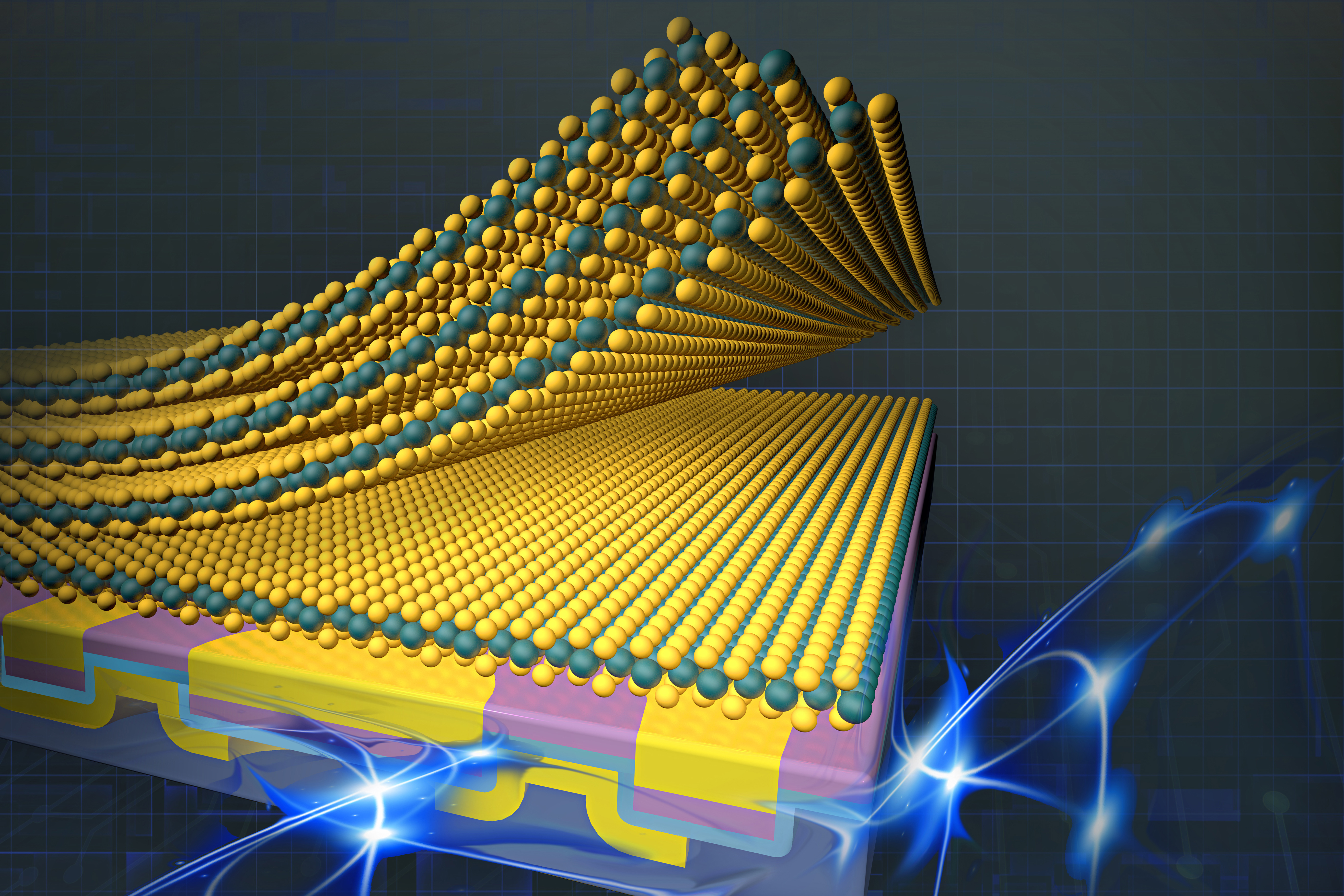
Researchers from MIT and the University of Texas at Austin took a major step toward making this idea a reality by demonstrating the first chip-based 3D printer. Their proof-of-concept device consists of a single, millimeter-scale photonic chip that emits reconfigurable beams of light into a well of resin that cures into a solid shape when light strikes it.

The prototype chip has no moving parts, instead relying on an array of tiny optical antennas to steer a beam of light. The beam projects up into a liquid resin that has been designed to rapidly cure when exposed to the beam’s wavelength of visible light.

By combining silicon photonics and photochemistry, the interdisciplinary research team was able to demonstrate a chip that can steer light beams to 3D print arbitrary two-dimensional patterns, including the letters M-I-T. Shapes can be fully formed in a matter of seconds.

In the long run, they envision a system where a photonic chip sits at the bottom of a well of resin and emits a 3D hologram of visible light, rapidly curing an entire object in a single step.

This type of portable 3D printer could have many applications, such as enabling clinicians to create tailor-made medical device components or allowing engineers to make rapid prototypes at a job site.

“This system is completely rethinking what a 3D printer is. It is no longer a big box sitting on a bench in a lab creating objects, but something that is handheld and portable. It is exciting to think about the new applications that could come out of this and how the field of 3D printing could change,” says senior author Jelena Notaros, the Robert J. Shillman Career Development Professor in Electrical Engineering and Computer Science (EECS), and a member of the Research Laboratory of Electronics.

Joining Notaros on the paper are Sabrina Corsetti, lead author and EECS graduate student; Milica Notaros PhD ’23; Tal Sneh, an EECS graduate student; Alex Safford, a recent graduate of the University of Texas at Austin; and Zak Page, an assistant professor in the Department of Chemical Engineering at UT Austin. The research appears today in Nature Light Science and Applications.

Printing with a chip

Experts in silicon photonics, the Notaros group previously developed integrated optical-phased-array systems that steer beams of light using a series of microscale antennas fabricated on a chip using semiconductor manufacturing processes. By speeding up or delaying the optical signal on either side of the antenna array, they can move the beam of emitted light in a certain direction.

Such systems are key for lidar sensors, which map their surroundings by emitting infrared light beams that bounce off nearby objects. Recently, the group has focused on systems that emit and steer visible light for augmented-reality applications.

They wondered if such a device could be used for a chip-based 3D printer.

At about the same time they started brainstorming, the Page Group at UT Austin demonstrated specialized resins that can be rapidly cured using wavelengths of visible light for the first time. This was the missing piece that pushed the chip-based 3D printer into reality.

“With photocurable resins, it is very hard to get them to cure all the way up at infrared wavelengths, which is where integrated optical-phased-array systems were operating in the past for lidar,” Corsetti says. “Here, we are meeting in the middle between standard photochemistry and silicon photonics by using visible-light-curable resins and visible-light-emitting chips to create this chip-based 3D printer. You have this merging of two technologies into a completely new idea.”

Their prototype consists of a single photonic chip containing an array of 160-nanometer-thick optical antennas. (A sheet of paper is about 100,000 nanometers thick.) The entire chip fits onto a U.S. quarter.

When powered by an off-chip laser, the antennas emit a steerable beam of visible light into the well of photocurable resin. The chip sits below a clear slide, like those used in microscopes, which contains a shallow indentation that holds the resin. The researchers use electrical signals to nonmechanically steer the light beam, causing the resin to solidify wherever the beam strikes it.

A collaborative approach

But effectively modulating visible-wavelength light, which involves modifying its amplitude and phase, is especially tricky. One common method requires heating the chip, but this is inefficient and takes a large amount of physical space.

Instead, the researchers used liquid crystal to fashion compact modulators they integrate onto the chip. The material’s unique optical properties enable the modulators to be extremely efficient and only about 20 microns in length.

A single waveguide on the chip holds the light from the off-chip laser. Running along the waveguide are tiny taps which tap off a little bit of light to each of the antennas.

The researchers actively tune the modulators using an electric field, which reorients the liquid crystal molecules in a certain direction. In this way, they can precisely control the amplitude and phase of light being routed to the antennas.

But forming and steering the beam is only half the battle. Interfacing with a novel photocurable resin was a completely different challenge.

The Page Group at UT Austin worked closely with the Notaros Group at MIT, carefully adjusting the chemical combinations and concentrations to zero-in on a formula that provided a long shelf-life and rapid curing.

In the end, the group used their prototype to 3D print arbitrary two-dimensional shapes within seconds.

Building off this prototype, they want to move toward developing a system like the one they originally conceptualized — a chip that emits a hologram of visible light in a resin well to enable volumetric 3D printing in only one step.

“To be able to do that, we need a completely new silicon-photonics chip design. We already laid out a lot of what that final system would look like in this paper. And, now, we are excited to continue working towards this ultimate demonstration,” Jelena Notaros says.

This work was funded, in part, by the U.S. National Science Foundation, the U.S. Defense Advanced Research Projects Agency, the Robert A. Welch Foundation, the MIT Rolf G. Locher Endowed Fellowship, and the MIT Frederick and Barbara Cronin Fellowship.

© Credit: Sampson Wilcox, RLE

The tiny device could enable a user to rapidly create customized, low-cost objects on the go, like a fastener to repair a wobbly bicycle wheel or a component for a critical medical operation.

Turning up the heat on next-generation semiconductors

The scorching surface of Venus, where temperatures can climb to 480 degrees Celsius (hot enough to melt lead), is an inhospitable place for humans and machines alike. One reason scientists have not yet been able to send a rover to the planet’s surface is because silicon-based electronics can’t operate in such extreme temperatures for an extended period of time.

For high-temperature applications like Venus exploration, researchers have recently turned to gallium nitride, a unique material that can withstand temperatures of 500 degrees or more.

The material is already used in some terrestrial electronics, like phone chargers and cell phone towers, but scientists don’t have a good grasp of how gallium nitride devices would behave at temperatures beyond 300 degrees, which is the operational limit of conventional silicon electronics.

In a new paper published in Applied Physics Letterswhich is part of a multiyear research effort, a team of scientists from MIT and elsewhere sought to answer key questions about the material’s properties and performance at extremely high temperatures.  

They studied the impact of temperature on the ohmic contacts in a gallium nitride device. Ohmic contacts are key components that connect a semiconductor device with the outside world.

The researchers found that extreme temperatures didn’t cause significant degradation to the gallium nitride material or contacts. They were surprised to see that the contacts remained structurally intact even when held at 500 degrees Celsius for 48 hours.

Understanding how contacts perform at extreme temperatures is an important step toward the group’s next goal of developing high-performance transistors that could operate on the surface of Venus. Such transistors could also be used on Earth in electronics for applications like extracting geothermal energy or monitoring the inside of jet engines.

“Transistors are the heart of most modern electronics, but we didn’t want to jump straight to making a gallium nitride transistor because so much could go wrong. We first wanted to make sure the material and contacts could survive, and figure out how much they change as you increase the temperature. We’ll design our transistor from these basic material building blocks,” says John Niroula, an electrical engineering and computer science (EECS) graduate student and lead author of the paper.

His co-authors include Qingyun Xie PhD ’24; Mengyang Yuan PhD ’22; EECS graduate students Patrick K. Darmawi-Iskandar and Pradyot Yadav; Gillian K. Micale, a graduate student in the Department of Materials Science and Engineering; senior author Tomás Palacios, the Clarence J. LeBel Professor of EECS, director of the Microsystems Technology Laboratories, and a member of the Research Laboratory of Electronics; as well as collaborators Nitul S. Rajput of the Technology Innovation Institute of the United Arab Emirates; Siddharth Rajan of Ohio State University; Yuji Zhao of Rice University; and Nadim Chowdhury of Bangladesh University of Engineering and Technology.

Turning up the heat

While gallium nitride has recently attracted much attention, the material is still decades behind silicon when it comes to scientists’ understanding of how its properties change under different conditions. One such property is resistance, the flow of electrical current through a material.

A device’s overall resistance is inversely proportional to its size. But devices like semiconductors have contacts that connect them to other electronics. Contact resistance, which is caused by these electrical connections, remains fixed no matter the size of the device. Too much contact resistance can lead to higher power dissipation and slower operating frequencies for electronic circuits.

“Especially when you go to smaller dimensions, a device’s performance often ends up being limited by contact resistance. People have a relatively good understanding of contact resistance at room temperature, but no one has really studied what happens when you go all the way up to 500 degrees,” Niroula says.

For their study, the researchers used facilities at MIT.nano to build gallium nitride devices known as transfer length method structures, which are composed of a series of resistors. These devices enable them to measure the resistance of both the material and the contacts.

They added ohmic contacts to these devices using the two most common methods. The first involves depositing metal onto gallium nitride and heating it to 825 degrees Celsius for about 30 seconds, a process called annealing.

The second method involves removing chunks of gallium nitride and using a high-temperature technology to regrow highly doped gallium nitride in its place, a process led by Rajan and his team at Ohio State. The highly doped material contains extra electrons that can contribute to current conduction.

“The regrowth method typically leads to lower contact resistance at room temperature, but we wanted to see if these methods still work well at high temperatures,” Niroula says.

A comprehensive approach

They tested devices in two ways. Their collaborators at Rice University, led by Zhao, conducted short-term tests by placing devices on a hot chuck that reached 500 degrees Celsius and taking immediate resistance measurements.

At MIT, they conducted longer-term experiments by placing devices into a specialized furnace the group previously developed. They left devices inside for up to 72 hours to measure how resistance changes as a function of temperature and time.

Microscopy experts at MIT.nano (Aubrey N. Penn) and the Technology Innovation Institute (Nitul S. Rajput) used state-of-the-art transmission electron microscopes to see how such high temperatures affect gallium nitride and the ohmic contacts at the atomic level.

“We went in thinking the contacts or the gallium nitride material itself would degrade significantly, but we found the opposite. Contacts made with both methods seemed to be remarkably stable,” says Niroula.

While it is difficult to measure resistance at such high temperatures, their results indicate that contact resistance seems to remain constant even at temperatures of 500 degrees, for around 48 hours. And just like at room temperature, the regrowth process led to better performance.

The material did start to degrade after being in the furnace for 48 hours, but the researchers are already working to boost long-term performance. One strategy involves adding protective insulators to keep the material from being directly exposed to the high-temperature environment.

Moving forward, the researchers plan to use what they learned in these experiments to develop high-temperature gallium nitride transistors.

“In our group, we focus on innovative, device-level research to advance the frontiers of microelectronics, while adopting a systematic approach across the hierarchy, from the material level to the circuit level. Here, we have gone all the way down to the material level to understand things in depth. In other words, we have translated device-level advancements to circuit-level impact for high-temperature electronics, through design, modeling and complex fabrication. We are also immensely fortunate to have forged close partnerships with our longtime collaborators in this journey,” Xie says.

This work was funded, in part, by the U.S. Air Force Office of Scientific Research, Lockheed Martin Corporation, the Semiconductor Research Corporation through the U.S. Defense Advanced Research Projects Agency, the U.S. Department of Energy, Intel Corporation, and the Bangladesh University of Engineering and Technology.

Fabrication and microscopy were conducted at MIT.nano, the Semiconductor Epitaxy and Analysis Laboratory at Ohio State University, the Center for Advanced Materials Characterization at the University of Oregon, and the Technology Innovation Institute of the United Arab Emirates.

© Image: MIT News; iStock

Researchers studied how temperatures up to 500 degrees Celsius would affect electronic devices made from gallium nitride, a key step in their multiyear research effort to develop electronics that can operate in extremely hot environments, like the surface of Venus.

Researchers harness 2D magnetic materials for energy-efficient computing

Experimental computer memories and processors built from magnetic materials use far less energy than traditional silicon-based devices. Two-dimensional magnetic materials, composed of layers that are only a few atoms thick, have incredible properties that could allow magnetic-based devices to achieve unprecedented speed, efficiency, and scalability.

While many hurdles must be overcome until these so-called van der Waals magnetic materials can be integrated into functioning computers, MIT researchers took an important step in this direction by demonstrating precise control of a van der Waals magnet at room temperature.

This is key, since magnets composed of atomically thin van der Waals materials can typically only be controlled at extremely cold temperatures, making them difficult to deploy outside a laboratory.

The researchers used pulses of electrical current to switch the direction of the device’s magnetization at room temperature. Magnetic switching can be used in computation, the same way a transistor switches between open and closed to represent 0s and 1s in binary code, or in computer memory, where switching enables data storage.

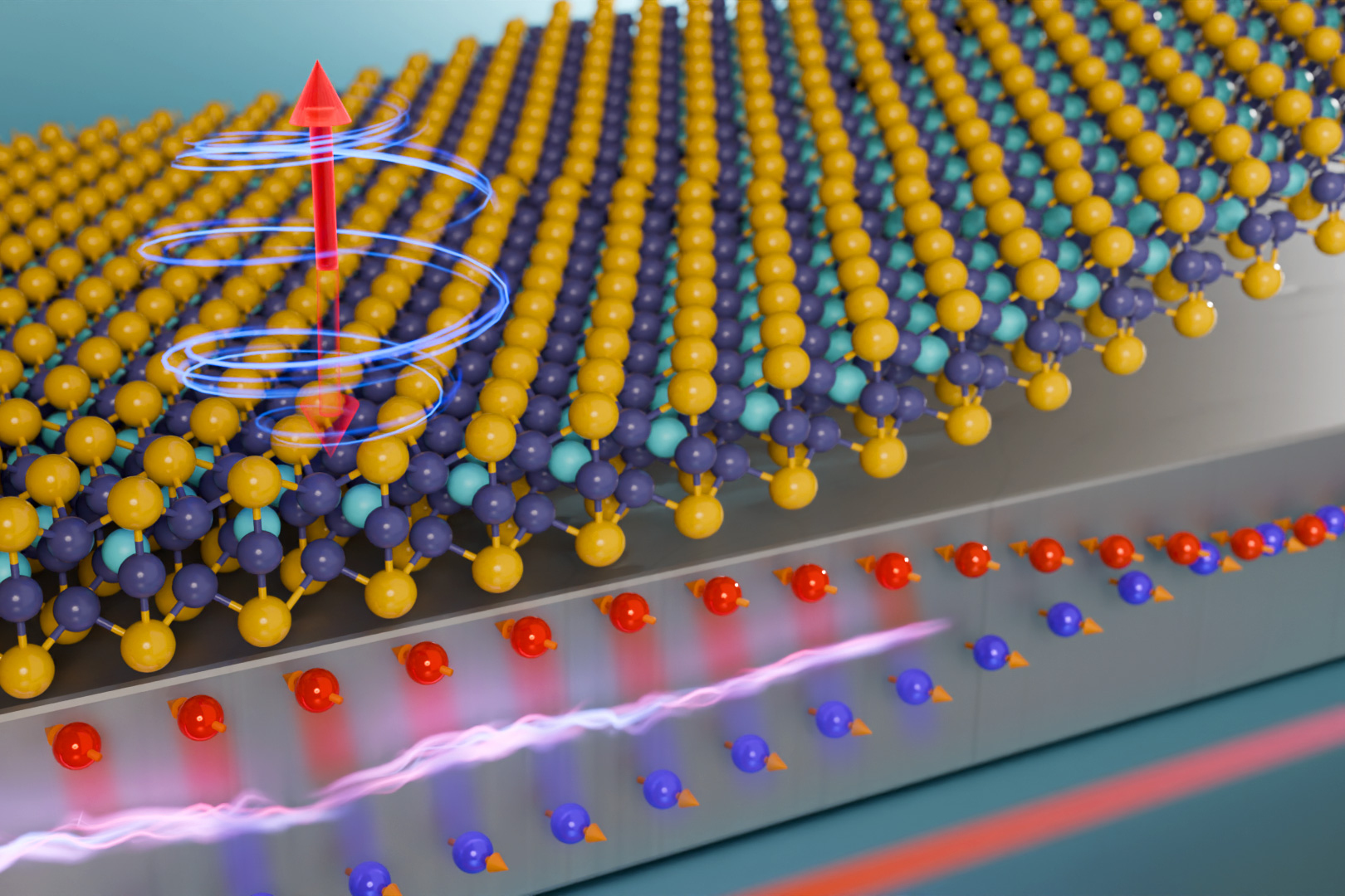
The team fired bursts of electrons at a magnet made of a new material that can sustain its magnetism at higher temperatures. The experiment leveraged a fundamental property of electrons known as spin, which makes the electrons behave like tiny magnets. By manipulating the spin of electrons that strike the device, the researchers can switch its magnetization.

“The heterostructure device we have developed requires an order of magnitude lower electrical current to switch the van der Waals magnet, compared to that required for bulk magnetic devices,” says Deblina Sarkar, the AT&T Career Development Assistant Professor in the MIT Media Lab and Center for Neurobiological Engineering, head of the Nano-Cybernetic Biotrek Lab, and the senior author of a paper on this technique. “Our device is also more energy efficient than other van der Waals magnets that are unable to switch at room temperature.”

In the future, such a magnet could be used to build faster computers that consume less electricity. It could also enable magnetic computer memories that are nonvolatile, which means they don’t leak information when powered off, or processors that make complex AI algorithms more energy-efficient.

“There is a lot of inertia around trying to improve materials that worked well in the past. But we have shown that if you make radical changes, starting by rethinking the materials you are using, you can potentially get much better solutions,” says Shivam Kajale, a graduate student in Sarkar’s lab and co-lead author of the paper.

Kajale and Sarkar are joined on the paper by co-lead author Thanh Nguyen, a graduate student in the Department of Nuclear Science and Engineering (NSE); Corson Chao, a graduate student in the Department of Materials Science and Engineering (DSME); David Bono, a DSME research scientist; Artittaya Boonkird, an NSE graduate student; and Mingda Li, associate professor of nuclear science and engineering. The research appears this week in Nature Communications.

An atomically thin advantage

Methods to fabricate tiny computer chips in a clean room from bulk materials like silicon can hamper devices. For instance, the layers of material may be barely 1 nanometer thick, so minuscule rough spots on the surface can be severe enough to degrade performance.

By contrast, van der Waals magnetic materials are intrinsically layered and structured in such a way that the surface remains perfectly smooth, even as researchers peel off layers to make thinner devices. In addition, atoms in one layer won’t leak into other layers, enabling the materials to retain their unique properties when stacked in devices.

“In terms of scaling and making these magnetic devices competitive for commercial applications, van der Waals materials are the way to go,” Kajale says.

But there’s a catch. This new class of magnetic materials have typically only been operated at temperatures below 60 kelvins (-351 degrees Fahrenheit). To build a magnetic computer processor or memory, researchers need to use electrical current to operate the magnet at room temperature.

To achieve this, the team focused on an emerging material called iron gallium telluride. This atomically thin material has all the properties needed for effective room temperature magnetism and doesn’t contain rare earth elements, which are undesirable because extracting them is especially destructive to the environment.

Nguyen carefully grew bulk crystals of this 2D material using a special technique. Then, Kajale fabricated a two-layer magnetic device using nanoscale flakes of iron gallium telluride underneath a six-nanometer layer of platinum.

Tiny device in hand, they used an intrinsic property of electrons known as spin to switch its magnetization at room temperature.

Electron ping-pong

While electrons don’t technically “spin” like a top, they do possess the same kind of angular momentum. That spin has a direction, either up or down. The researchers can leverage a property known as spin-orbit coupling to control the spins of electrons they fire at the magnet.

The same way momentum is transferred when one ball hits another, electrons will transfer their “spin momentum” to the 2D magnetic material when they strike it. Depending on the direction of their spins, that momentum transfer can reverse the magnetization.

In a sense, this transfer rotates the magnetization from up to down (or vice-versa), so it is called a “torque,” as in spin-orbit torque switching. Applying a negative electric pulse causes the magnetization to go downward, while a positive pulse causes it to go upward.

The researchers can do this switching at room temperature for two reasons: the special properties of iron gallium telluride and the fact that their technique uses small amounts of electrical current. Pumping too much current into the device would cause it to overheat and demagnetize.

The team faced many challenges over the two years it took to achieve this milestone, Kajale says. Finding the right magnetic material was only half the battle. Since iron gallium telluride oxidizes quickly, fabrication must be done inside a glovebox filled with nitrogen.

“The device is only exposed to air for 10 or 15 seconds, but even after that I have to do a step where I polish it to remove any oxide,” he says.

Now that they have demonstrated room-temperature switching and greater energy efficiency, the researchers plan to keep pushing the performance of magnetic van der Waals materials.

“Our next milestone is to achieve switching without the need for any external magnetic fields. Our aim is to enhance our technology and scale up to bring the versatility of van der Waals magnet to commercial applications,” Sarkar says.

This work was carried out, in part, using the facilities at MIT.Nano and the Harvard University Center for Nanoscale Systems.

© Image: Courtesy of the researchers

This illustration shows electric current being pumped into platinum (the bottom slab), which results in the creation of an electron spin current that switches the magnetic state of the 2D ferromagnet on top. The colored spheres represent the atoms in the 2D material.

Technique could improve the sensitivity of quantum sensing devices

In quantum sensing, atomic-scale quantum systems are used to measure electromagnetic fields, as well as properties like rotation, acceleration, and distance, far more precisely than classical sensors can. The technology could enable devices that image the brain with unprecedented detail, for example, or air traffic control systems with precise positioning accuracy.

As many real-world quantum sensing devices are emerging, one promising direction is the use of microscopic defects inside diamonds to create “qubits” that can be used for quantum sensing. Qubits are the building blocks of quantum devices.

Researchers at MIT and elsewhere have developed a technique that enables them to identify and control a greater number of these microscopic defects. This could help them build a larger system of qubits that can perform quantum sensing with greater sensitivity.

Their method builds off a central defect inside a diamond, known as a nitrogen-vacancy (NV) center, which scientists can detect and excite using laser light and then control with microwave pulses. This new approach uses a specific protocol of microwave pulses to identify and extend that control to additional defects that can’t be seen with a laser, which are called dark spins.

The researchers seek to control larger numbers of dark spins by locating them through a network of connected spins. Starting from this central NV spin, the researchers build this chain by coupling the NV spin to a nearby dark spin, and then use this dark spin as a probe to find and control a more distant spin which can’t be sensed by the NV directly. The process can be repeated on these more distant spins to control longer chains.

“One lesson I learned from this work is that searching in the dark may be quite discouraging when you don’t see results, but we were able to take this risk. It is possible, with some courage, to search in places that people haven’t looked before and find potentially more advantageous qubits,” says Alex Ungar, a PhD student in electrical engineering and computer science and a member of the Quantum Engineering Group at MIT, who is lead author of a paper on this technique, which is published today in PRX Quantum.

His co-authors include his advisor and corresponding author, Paola Cappellaro, the Ford Professor of Engineering in the Department of Nuclear Science and Engineering and professor of physics; as well as Alexandre Cooper, a senior research scientist at the University of Waterloo’s Institute for Quantum Computing; and Won Kyu Calvin Sun, a former researcher in Cappellaro’s group who is now a postdoc at the University of Illinois at Urbana-Champaign.

Diamond defects

To create NV centers, scientists implant nitrogen into a sample of diamond.

But introducing nitrogen into the diamond creates other types of atomic defects in the surrounding environment. Some of these defects, including the NV center, can host what are known as electronic spins, which originate from the valence electrons around the site of the defect. Valence electrons are those in the outermost shell of an atom. A defect’s interaction with an external magnetic field can be used to form a qubit.

Researchers can harness these electronic spins from neighboring defects to create more qubits around a single NV center. This larger collection of qubits is known as a quantum register. Having a larger quantum register boosts the performance of a quantum sensor.

Some of these electronic spin defects are connected to the NV center through magnetic interaction. In past work, researchers used this interaction to identify and control nearby spins. However, this approach is limited because the NV center is only stable for a short amount of time, a principle called coherence. It can only be used to control the few spins that can be reached within this coherence limit.

In this new paper, the researchers use an electronic spin defect that is near the NV center as a probe to find and control an additional spin, creating a chain of three qubits.

They use a technique known as spin echo double resonance (SEDOR), which involves a series of microwave pulses that decouple an NV center from all electronic spins that are interacting with it. Then, they selectively apply another microwave pulse to pair the NV center with one nearby spin.

Unlike the NV, these neighboring dark spins can’t be excited, or polarized, with laser light. This polarization is a required step to control them with microwaves.

Once the researchers find and characterize a first-layer spin, they can transfer the NV’s polarization to this first-layer spin through the magnetic interaction by applying microwaves to both spins simultaneously. Then once the first-layer spin is polarized, they repeat the SEDOR process on the first-layer spin, using it as a probe to identify a second-layer spin that is interacting with it.

Controlling a chain of dark spins

This repeated SEDOR process allows the researchers to detect and characterize a new, distinct defect located outside the coherence limit of the NV center. To control this more distant spin, they carefully apply a specific series of microwave pulses that enable them to transfer the polarization from the NV center along the chain to this second-layer spin.

“This is setting the stage for building larger quantum registers to higher-layer spins or longer spin chains, and also showing that we can find these new defects that weren’t discovered before by scaling up this technique,” Ungar says.

To control a spin, the microwave pulses must be very close to the resonance frequency of that spin. Tiny drifts in the experimental setup, due to temperature or vibrations, can throw off the microwave pulses.

The researchers were able to optimize their protocol for sending precise microwave pulses, which enabled them to effectively identify and control second-layer spins, Ungar says.

“We are searching for something in the unknown, but at the same time, the environment might not be stable, so you don’t know if what you are finding is just noise. Once you start seeing promising things, you can put all your best effort in that one direction. But before you arrive there, it is a leap of faith,” Cappellaro says.

While they were able to effectively demonstrate a three-spin chain, the researchers estimate they could scale their method to a fifth layer using their current protocol, which could provide access to hundreds of potential qubits. With further optimization, they may be able to scale up to more than 10 layers.

In the future, they plan to continue enhancing their technique to efficiently characterize and probe other electronic spins in the environment and explore different types of defects that could be used to form qubits.

This research is supported, in part, by the U.S. National Science Foundation and the Canada First Research Excellence Fund.

© Image: Courtesy of the researchers

Researchers use microscopic defects inside a diamond to build a chain of three qubits (pictured as small circles with arrows) that they can use for quantum sensing. They start from a central defect, couple it with a nearby defect, and then use this second defect to find and control a third defect.

Researchers demonstrate the first chip-based 3D printer

Imagine a portable 3D printer you could hold in the palm of your hand. The tiny device could enable a user to rapidly create customized, low-cost objects on the go, like a fastener to repair a wobbly bicycle wheel or a component for a critical medical operation.

Researchers from MIT and the University of Texas at Austin took a major step toward making this idea a reality by demonstrating the first chip-based 3D printer. Their proof-of-concept device consists of a single, millimeter-scale photonic chip that emits reconfigurable beams of light into a well of resin that cures into a solid shape when light strikes it.

The prototype chip has no moving parts, instead relying on an array of tiny optical antennas to steer a beam of light. The beam projects up into a liquid resin that has been designed to rapidly cure when exposed to the beam’s wavelength of visible light.

By combining silicon photonics and photochemistry, the interdisciplinary research team was able to demonstrate a chip that can steer light beams to 3D print arbitrary two-dimensional patterns, including the letters M-I-T. Shapes can be fully formed in a matter of seconds.

In the long run, they envision a system where a photonic chip sits at the bottom of a well of resin and emits a 3D hologram of visible light, rapidly curing an entire object in a single step.

This type of portable 3D printer could have many applications, such as enabling clinicians to create tailor-made medical device components or allowing engineers to make rapid prototypes at a job site.

“This system is completely rethinking what a 3D printer is. It is no longer a big box sitting on a bench in a lab creating objects, but something that is handheld and portable. It is exciting to think about the new applications that could come out of this and how the field of 3D printing could change,” says senior author Jelena Notaros, the Robert J. Shillman Career Development Professor in Electrical Engineering and Computer Science (EECS), and a member of the Research Laboratory of Electronics.

Joining Notaros on the paper are Sabrina Corsetti, lead author and EECS graduate student; Milica Notaros PhD ’23; Tal Sneh, an EECS graduate student; Alex Safford, a recent graduate of the University of Texas at Austin; and Zak Page, an assistant professor in the Department of Chemical Engineering at UT Austin. The research appears today in Nature Light Science and Applications.

Printing with a chip

Experts in silicon photonics, the Notaros group previously developed integrated optical-phased-array systems that steer beams of light using a series of microscale antennas fabricated on a chip using semiconductor manufacturing processes. By speeding up or delaying the optical signal on either side of the antenna array, they can move the beam of emitted light in a certain direction.

Such systems are key for lidar sensors, which map their surroundings by emitting infrared light beams that bounce off nearby objects. Recently, the group has focused on systems that emit and steer visible light for augmented-reality applications.

They wondered if such a device could be used for a chip-based 3D printer.

At about the same time they started brainstorming, the Page Group at UT Austin demonstrated specialized resins that can be rapidly cured using wavelengths of visible light for the first time. This was the missing piece that pushed the chip-based 3D printer into reality.

“With photocurable resins, it is very hard to get them to cure all the way up at infrared wavelengths, which is where integrated optical-phased-array systems were operating in the past for lidar,” Corsetti says. “Here, we are meeting in the middle between standard photochemistry and silicon photonics by using visible-light-curable resins and visible-light-emitting chips to create this chip-based 3D printer. You have this merging of two technologies into a completely new idea.”

Their prototype consists of a single photonic chip containing an array of 160-nanometer-thick optical antennas. (A sheet of paper is about 100,000 nanometers thick.) The entire chip fits onto a U.S. quarter.

When powered by an off-chip laser, the antennas emit a steerable beam of visible light into the well of photocurable resin. The chip sits below a clear slide, like those used in microscopes, which contains a shallow indentation that holds the resin. The researchers use electrical signals to nonmechanically steer the light beam, causing the resin to solidify wherever the beam strikes it.

A collaborative approach

But effectively modulating visible-wavelength light, which involves modifying its amplitude and phase, is especially tricky. One common method requires heating the chip, but this is inefficient and takes a large amount of physical space.

Instead, the researchers used liquid crystal to fashion compact modulators they integrate onto the chip. The material’s unique optical properties enable the modulators to be extremely efficient and only about 20 microns in length.

A single waveguide on the chip holds the light from the off-chip laser. Running along the waveguide are tiny taps which tap off a little bit of light to each of the antennas.

The researchers actively tune the modulators using an electric field, which reorients the liquid crystal molecules in a certain direction. In this way, they can precisely control the amplitude and phase of light being routed to the antennas.

But forming and steering the beam is only half the battle. Interfacing with a novel photocurable resin was a completely different challenge.

The Page Group at UT Austin worked closely with the Notaros Group at MIT, carefully adjusting the chemical combinations and concentrations to zero-in on a formula that provided a long shelf-life and rapid curing.

In the end, the group used their prototype to 3D print arbitrary two-dimensional shapes within seconds.

Building off this prototype, they want to move toward developing a system like the one they originally conceptualized — a chip that emits a hologram of visible light in a resin well to enable volumetric 3D printing in only one step.

“To be able to do that, we need a completely new silicon-photonics chip design. We already laid out a lot of what that final system would look like in this paper. And, now, we are excited to continue working towards this ultimate demonstration,” Jelena Notaros says.

This work was funded, in part, by the U.S. National Science Foundation, the U.S. Defense Advanced Research Projects Agency, the Robert A. Welch Foundation, the MIT Rolf G. Locher Endowed Fellowship, and the MIT Frederick and Barbara Cronin Fellowship.

© Credit: Sampson Wilcox, RLE
The tiny device could enable a user to rapidly create customized, low-cost objects on the go, like a fastener to repair a wobbly bicycle wheel or a component for a critical medical operation.

Turning up the heat on next-generation semiconductors

The scorching surface of Venus, where temperatures can climb to 480 degrees Celsius (hot enough to melt lead), is an inhospitable place for humans and machines alike. One reason scientists have not yet been able to send a rover to the planet’s surface is because silicon-based electronics can’t operate in such extreme temperatures for an extended period of time.

For high-temperature applications like Venus exploration, researchers have recently turned to gallium nitride, a unique material that can withstand temperatures of 500 degrees or more.

The material is already used in some terrestrial electronics, like phone chargers and cell phone towers, but scientists don’t have a good grasp of how gallium nitride devices would behave at temperatures beyond 300 degrees, which is the operational limit of conventional silicon electronics.

In a new paper published in Applied Physics Letterswhich is part of a multiyear research effort, a team of scientists from MIT and elsewhere sought to answer key questions about the material’s properties and performance at extremely high temperatures.  

They studied the impact of temperature on the ohmic contacts in a gallium nitride device. Ohmic contacts are key components that connect a semiconductor device with the outside world.

The researchers found that extreme temperatures didn’t cause significant degradation to the gallium nitride material or contacts. They were surprised to see that the contacts remained structurally intact even when held at 500 degrees Celsius for 48 hours.

Understanding how contacts perform at extreme temperatures is an important step toward the group’s next goal of developing high-performance transistors that could operate on the surface of Venus. Such transistors could also be used on Earth in electronics for applications like extracting geothermal energy or monitoring the inside of jet engines.

“Transistors are the heart of most modern electronics, but we didn’t want to jump straight to making a gallium nitride transistor because so much could go wrong. We first wanted to make sure the material and contacts could survive, and figure out how much they change as you increase the temperature. We’ll design our transistor from these basic material building blocks,” says John Niroula, an electrical engineering and computer science (EECS) graduate student and lead author of the paper.

His co-authors include Qingyun Xie PhD ’24; Mengyang Yuan PhD ’22; EECS graduate students Patrick K. Darmawi-Iskandar and Pradyot Yadav; Gillian K. Micale, a graduate student in the Department of Materials Science and Engineering; senior author Tomás Palacios, the Clarence J. LeBel Professor of EECS, director of the Microsystems Technology Laboratories, and a member of the Research Laboratory of Electronics; as well as collaborators Nitul S. Rajput of the Technology Innovation Institute of the United Arab Emirates; Siddharth Rajan of Ohio State University; Yuji Zhao of Rice University; and Nadim Chowdhury of Bangladesh University of Engineering and Technology.

Turning up the heat

While gallium nitride has recently attracted much attention, the material is still decades behind silicon when it comes to scientists’ understanding of how its properties change under different conditions. One such property is resistance, the flow of electrical current through a material.

A device’s overall resistance is inversely proportional to its size. But devices like semiconductors have contacts that connect them to other electronics. Contact resistance, which is caused by these electrical connections, remains fixed no matter the size of the device. Too much contact resistance can lead to higher power dissipation and slower operating frequencies for electronic circuits.

“Especially when you go to smaller dimensions, a device’s performance often ends up being limited by contact resistance. People have a relatively good understanding of contact resistance at room temperature, but no one has really studied what happens when you go all the way up to 500 degrees,” Niroula says.

For their study, the researchers used facilities at MIT.nano to build gallium nitride devices known as transfer length method structures, which are composed of a series of resistors. These devices enable them to measure the resistance of both the material and the contacts.

They added ohmic contacts to these devices using the two most common methods. The first involves depositing metal onto gallium nitride and heating it to 825 degrees Celsius for about 30 seconds, a process called annealing.

The second method involves removing chunks of gallium nitride and using a high-temperature technology to regrow highly doped gallium nitride in its place, a process led by Rajan and his team at Ohio State. The highly doped material contains extra electrons that can contribute to current conduction.

“The regrowth method typically leads to lower contact resistance at room temperature, but we wanted to see if these methods still work well at high temperatures,” Niroula says.

A comprehensive approach

They tested devices in two ways. Their collaborators at Rice University, led by Zhao, conducted short-term tests by placing devices on a hot chuck that reached 500 degrees Celsius and taking immediate resistance measurements.

At MIT, they conducted longer-term experiments by placing devices into a specialized furnace the group previously developed. They left devices inside for up to 72 hours to measure how resistance changes as a function of temperature and time.

Microscopy experts at MIT.nano (Aubrey N. Penn) and the Technology Innovation Institute (Nitul S. Rajput) used state-of-the-art transmission electron microscopes to see how such high temperatures affect gallium nitride and the ohmic contacts at the atomic level.

“We went in thinking the contacts or the gallium nitride material itself would degrade significantly, but we found the opposite. Contacts made with both methods seemed to be remarkably stable,” says Niroula.

While it is difficult to measure resistance at such high temperatures, their results indicate that contact resistance seems to remain constant even at temperatures of 500 degrees, for around 48 hours. And just like at room temperature, the regrowth process led to better performance.

The material did start to degrade after being in the furnace for 48 hours, but the researchers are already working to boost long-term performance. One strategy involves adding protective insulators to keep the material from being directly exposed to the high-temperature environment.

Moving forward, the researchers plan to use what they learned in these experiments to develop high-temperature gallium nitride transistors.

“In our group, we focus on innovative, device-level research to advance the frontiers of microelectronics, while adopting a systematic approach across the hierarchy, from the material level to the circuit level. Here, we have gone all the way down to the material level to understand things in depth. In other words, we have translated device-level advancements to circuit-level impact for high-temperature electronics, through design, modeling and complex fabrication. We are also immensely fortunate to have forged close partnerships with our longtime collaborators in this journey,” Xie says.

This work was funded, in part, by the U.S. Air Force Office of Scientific Research, Lockheed Martin Corporation, the Semiconductor Research Corporation through the U.S. Defense Advanced Research Projects Agency, the U.S. Department of Energy, Intel Corporation, and the Bangladesh University of Engineering and Technology.

Fabrication and microscopy were conducted at MIT.nano, the Semiconductor Epitaxy and Analysis Laboratory at Ohio State University, the Center for Advanced Materials Characterization at the University of Oregon, and the Technology Innovation Institute of the United Arab Emirates.

© Image: MIT News; iStock

Researchers studied how temperatures up to 500 degrees Celsius would affect electronic devices made from gallium nitride, a key step in their multiyear research effort to develop electronics that can operate in extremely hot environments, like the surface of Venus.

Researchers harness 2D magnetic materials for energy-efficient computing

Experimental computer memories and processors built from magnetic materials use far less energy than traditional silicon-based devices. Two-dimensional magnetic materials, composed of layers that are only a few atoms thick, have incredible properties that could allow magnetic-based devices to achieve unprecedented speed, efficiency, and scalability.

While many hurdles must be overcome until these so-called van der Waals magnetic materials can be integrated into functioning computers, MIT researchers took an important step in this direction by demonstrating precise control of a van der Waals magnet at room temperature.

This is key, since magnets composed of atomically thin van der Waals materials can typically only be controlled at extremely cold temperatures, making them difficult to deploy outside a laboratory.

The researchers used pulses of electrical current to switch the direction of the device’s magnetization at room temperature. Magnetic switching can be used in computation, the same way a transistor switches between open and closed to represent 0s and 1s in binary code, or in computer memory, where switching enables data storage.

The team fired bursts of electrons at a magnet made of a new material that can sustain its magnetism at higher temperatures. The experiment leveraged a fundamental property of electrons known as spin, which makes the electrons behave like tiny magnets. By manipulating the spin of electrons that strike the device, the researchers can switch its magnetization.

“The heterostructure device we have developed requires an order of magnitude lower electrical current to switch the van der Waals magnet, compared to that required for bulk magnetic devices,” says Deblina Sarkar, the AT&T Career Development Assistant Professor in the MIT Media Lab and Center for Neurobiological Engineering, head of the Nano-Cybernetic Biotrek Lab, and the senior author of a paper on this technique. “Our device is also more energy efficient than other van der Waals magnets that are unable to switch at room temperature.”

In the future, such a magnet could be used to build faster computers that consume less electricity. It could also enable magnetic computer memories that are nonvolatile, which means they don’t leak information when powered off, or processors that make complex AI algorithms more energy-efficient.

“There is a lot of inertia around trying to improve materials that worked well in the past. But we have shown that if you make radical changes, starting by rethinking the materials you are using, you can potentially get much better solutions,” says Shivam Kajale, a graduate student in Sarkar’s lab and co-lead author of the paper.

Kajale and Sarkar are joined on the paper by co-lead author Thanh Nguyen, a graduate student in the Department of Nuclear Science and Engineering (NSE); Corson Chao, a graduate student in the Department of Materials Science and Engineering (DSME); David Bono, a DSME research scientist; Artittaya Boonkird, an NSE graduate student; and Mingda Li, associate professor of nuclear science and engineering. The research appears this week in Nature Communications.

An atomically thin advantage

Methods to fabricate tiny computer chips in a clean room from bulk materials like silicon can hamper devices. For instance, the layers of material may be barely 1 nanometer thick, so minuscule rough spots on the surface can be severe enough to degrade performance.

By contrast, van der Waals magnetic materials are intrinsically layered and structured in such a way that the surface remains perfectly smooth, even as researchers peel off layers to make thinner devices. In addition, atoms in one layer won’t leak into other layers, enabling the materials to retain their unique properties when stacked in devices.

“In terms of scaling and making these magnetic devices competitive for commercial applications, van der Waals materials are the way to go,” Kajale says.

But there’s a catch. This new class of magnetic materials have typically only been operated at temperatures below 60 kelvins (-351 degrees Fahrenheit). To build a magnetic computer processor or memory, researchers need to use electrical current to operate the magnet at room temperature.

To achieve this, the team focused on an emerging material called iron gallium telluride. This atomically thin material has all the properties needed for effective room temperature magnetism and doesn’t contain rare earth elements, which are undesirable because extracting them is especially destructive to the environment.

Nguyen carefully grew bulk crystals of this 2D material using a special technique. Then, Kajale fabricated a two-layer magnetic device using nanoscale flakes of iron gallium telluride underneath a six-nanometer layer of platinum.

Tiny device in hand, they used an intrinsic property of electrons known as spin to switch its magnetization at room temperature.

Electron ping-pong

While electrons don’t technically “spin” like a top, they do possess the same kind of angular momentum. That spin has a direction, either up or down. The researchers can leverage a property known as spin-orbit coupling to control the spins of electrons they fire at the magnet.

The same way momentum is transferred when one ball hits another, electrons will transfer their “spin momentum” to the 2D magnetic material when they strike it. Depending on the direction of their spins, that momentum transfer can reverse the magnetization.

In a sense, this transfer rotates the magnetization from up to down (or vice-versa), so it is called a “torque,” as in spin-orbit torque switching. Applying a negative electric pulse causes the magnetization to go downward, while a positive pulse causes it to go upward.

The researchers can do this switching at room temperature for two reasons: the special properties of iron gallium telluride and the fact that their technique uses small amounts of electrical current. Pumping too much current into the device would cause it to overheat and demagnetize.

The team faced many challenges over the two years it took to achieve this milestone, Kajale says. Finding the right magnetic material was only half the battle. Since iron gallium telluride oxidizes quickly, fabrication must be done inside a glovebox filled with nitrogen.

“The device is only exposed to air for 10 or 15 seconds, but even after that I have to do a step where I polish it to remove any oxide,” he says.

Now that they have demonstrated room-temperature switching and greater energy efficiency, the researchers plan to keep pushing the performance of magnetic van der Waals materials.

“Our next milestone is to achieve switching without the need for any external magnetic fields. Our aim is to enhance our technology and scale up to bring the versatility of van der Waals magnet to commercial applications,” Sarkar says.

This work was carried out, in part, using the facilities at MIT.Nano and the Harvard University Center for Nanoscale Systems.

© Image: Courtesy of the researchers

This illustration shows electric current being pumped into platinum (the bottom slab), which results in the creation of an electron spin current that switches the magnetic state of the 2D ferromagnet on top. The colored spheres represent the atoms in the 2D material.

Technique could improve the sensitivity of quantum sensing devices

In quantum sensing, atomic-scale quantum systems are used to measure electromagnetic fields, as well as properties like rotation, acceleration, and distance, far more precisely than classical sensors can. The technology could enable devices that image the brain with unprecedented detail, for example, or air traffic control systems with precise positioning accuracy.

As many real-world quantum sensing devices are emerging, one promising direction is the use of microscopic defects inside diamonds to create “qubits” that can be used for quantum sensing. Qubits are the building blocks of quantum devices.

Researchers at MIT and elsewhere have developed a technique that enables them to identify and control a greater number of these microscopic defects. This could help them build a larger system of qubits that can perform quantum sensing with greater sensitivity.

Their method builds off a central defect inside a diamond, known as a nitrogen-vacancy (NV) center, which scientists can detect and excite using laser light and then control with microwave pulses. This new approach uses a specific protocol of microwave pulses to identify and extend that control to additional defects that can’t be seen with a laser, which are called dark spins.

The researchers seek to control larger numbers of dark spins by locating them through a network of connected spins. Starting from this central NV spin, the researchers build this chain by coupling the NV spin to a nearby dark spin, and then use this dark spin as a probe to find and control a more distant spin which can’t be sensed by the NV directly. The process can be repeated on these more distant spins to control longer chains.

“One lesson I learned from this work is that searching in the dark may be quite discouraging when you don’t see results, but we were able to take this risk. It is possible, with some courage, to search in places that people haven’t looked before and find potentially more advantageous qubits,” says Alex Ungar, a PhD student in electrical engineering and computer science and a member of the Quantum Engineering Group at MIT, who is lead author of a paper on this technique, which is published today in PRX Quantum.

His co-authors include his advisor and corresponding author, Paola Cappellaro, the Ford Professor of Engineering in the Department of Nuclear Science and Engineering and professor of physics; as well as Alexandre Cooper, a senior research scientist at the University of Waterloo’s Institute for Quantum Computing; and Won Kyu Calvin Sun, a former researcher in Cappellaro’s group who is now a postdoc at the University of Illinois at Urbana-Champaign.

Diamond defects

To create NV centers, scientists implant nitrogen into a sample of diamond.

But introducing nitrogen into the diamond creates other types of atomic defects in the surrounding environment. Some of these defects, including the NV center, can host what are known as electronic spins, which originate from the valence electrons around the site of the defect. Valence electrons are those in the outermost shell of an atom. A defect’s interaction with an external magnetic field can be used to form a qubit.

Researchers can harness these electronic spins from neighboring defects to create more qubits around a single NV center. This larger collection of qubits is known as a quantum register. Having a larger quantum register boosts the performance of a quantum sensor.

Some of these electronic spin defects are connected to the NV center through magnetic interaction. In past work, researchers used this interaction to identify and control nearby spins. However, this approach is limited because the NV center is only stable for a short amount of time, a principle called coherence. It can only be used to control the few spins that can be reached within this coherence limit.

In this new paper, the researchers use an electronic spin defect that is near the NV center as a probe to find and control an additional spin, creating a chain of three qubits.

They use a technique known as spin echo double resonance (SEDOR), which involves a series of microwave pulses that decouple an NV center from all electronic spins that are interacting with it. Then, they selectively apply another microwave pulse to pair the NV center with one nearby spin.

Unlike the NV, these neighboring dark spins can’t be excited, or polarized, with laser light. This polarization is a required step to control them with microwaves.

Once the researchers find and characterize a first-layer spin, they can transfer the NV’s polarization to this first-layer spin through the magnetic interaction by applying microwaves to both spins simultaneously. Then once the first-layer spin is polarized, they repeat the SEDOR process on the first-layer spin, using it as a probe to identify a second-layer spin that is interacting with it.

Controlling a chain of dark spins

This repeated SEDOR process allows the researchers to detect and characterize a new, distinct defect located outside the coherence limit of the NV center. To control this more distant spin, they carefully apply a specific series of microwave pulses that enable them to transfer the polarization from the NV center along the chain to this second-layer spin.

“This is setting the stage for building larger quantum registers to higher-layer spins or longer spin chains, and also showing that we can find these new defects that weren’t discovered before by scaling up this technique,” Ungar says.

To control a spin, the microwave pulses must be very close to the resonance frequency of that spin. Tiny drifts in the experimental setup, due to temperature or vibrations, can throw off the microwave pulses.

The researchers were able to optimize their protocol for sending precise microwave pulses, which enabled them to effectively identify and control second-layer spins, Ungar says.

“We are searching for something in the unknown, but at the same time, the environment might not be stable, so you don’t know if what you are finding is just noise. Once you start seeing promising things, you can put all your best effort in that one direction. But before you arrive there, it is a leap of faith,” Cappellaro says.

While they were able to effectively demonstrate a three-spin chain, the researchers estimate they could scale their method to a fifth layer using their current protocol, which could provide access to hundreds of potential qubits. With further optimization, they may be able to scale up to more than 10 layers.

In the future, they plan to continue enhancing their technique to efficiently characterize and probe other electronic spins in the environment and explore different types of defects that could be used to form qubits.

This research is supported, in part, by the U.S. National Science Foundation and the Canada First Research Excellence Fund.

© Image: Courtesy of the researchers

Researchers use microscopic defects inside a diamond to build a chain of three qubits (pictured as small circles with arrows) that they can use for quantum sensing. They start from a central defect, couple it with a nearby defect, and then use this second defect to find and control a third defect.

Researchers demonstrate the first chip-based 3D printer

Imagine a portable 3D printer you could hold in the palm of your hand. The tiny device could enable a user to rapidly create customized, low-cost objects on the go, like a fastener to repair a wobbly bicycle wheel or a component for a critical medical operation.

Researchers from MIT and the University of Texas at Austin took a major step toward making this idea a reality by demonstrating the first chip-based 3D printer. Their proof-of-concept device consists of a single, millimeter-scale photonic chip that emits reconfigurable beams of light into a well of resin that cures into a solid shape when light strikes it.

The prototype chip has no moving parts, instead relying on an array of tiny optical antennas to steer a beam of light. The beam projects up into a liquid resin that has been designed to rapidly cure when exposed to the beam’s wavelength of visible light.

By combining silicon photonics and photochemistry, the interdisciplinary research team was able to demonstrate a chip that can steer light beams to 3D print arbitrary two-dimensional patterns, including the letters M-I-T. Shapes can be fully formed in a matter of seconds.

In the long run, they envision a system where a photonic chip sits at the bottom of a well of resin and emits a 3D hologram of visible light, rapidly curing an entire object in a single step.

This type of portable 3D printer could have many applications, such as enabling clinicians to create tailor-made medical device components or allowing engineers to make rapid prototypes at a job site.

“This system is completely rethinking what a 3D printer is. It is no longer a big box sitting on a bench in a lab creating objects, but something that is handheld and portable. It is exciting to think about the new applications that could come out of this and how the field of 3D printing could change,” says senior author Jelena Notaros, the Robert J. Shillman Career Development Professor in Electrical Engineering and Computer Science (EECS), and a member of the Research Laboratory of Electronics.

Joining Notaros on the paper are Sabrina Corsetti, lead author and EECS graduate student; Milica Notaros PhD ’23; Tal Sneh, an EECS graduate student; Alex Safford, a recent graduate of the University of Texas at Austin; and Zak Page, an assistant professor in the Department of Chemical Engineering at UT Austin. The research appears today in Nature Light Science and Applications.

Printing with a chip

Experts in silicon photonics, the Notaros group previously developed integrated optical-phased-array systems that steer beams of light using a series of microscale antennas fabricated on a chip using semiconductor manufacturing processes. By speeding up or delaying the optical signal on either side of the antenna array, they can move the beam of emitted light in a certain direction.

Such systems are key for lidar sensors, which map their surroundings by emitting infrared light beams that bounce off nearby objects. Recently, the group has focused on systems that emit and steer visible light for augmented-reality applications.

They wondered if such a device could be used for a chip-based 3D printer.

At about the same time they started brainstorming, the Page Group at UT Austin demonstrated specialized resins that can be rapidly cured using wavelengths of visible light for the first time. This was the missing piece that pushed the chip-based 3D printer into reality.

“With photocurable resins, it is very hard to get them to cure all the way up at infrared wavelengths, which is where integrated optical-phased-array systems were operating in the past for lidar,” Corsetti says. “Here, we are meeting in the middle between standard photochemistry and silicon photonics by using visible-light-curable resins and visible-light-emitting chips to create this chip-based 3D printer. You have this merging of two technologies into a completely new idea.”

Their prototype consists of a single photonic chip containing an array of 160-nanometer-thick optical antennas. (A sheet of paper is about 100,000 nanometers thick.) The entire chip fits onto a U.S. quarter.

When powered by an off-chip laser, the antennas emit a steerable beam of visible light into the well of photocurable resin. The chip sits below a clear slide, like those used in microscopes, which contains a shallow indentation that holds the resin. The researchers use electrical signals to nonmechanically steer the light beam, causing the resin to solidify wherever the beam strikes it.

A collaborative approach

But effectively modulating visible-wavelength light, which involves modifying its amplitude and phase, is especially tricky. One common method requires heating the chip, but this is inefficient and takes a large amount of physical space.

Instead, the researchers used liquid crystal to fashion compact modulators they integrate onto the chip. The material’s unique optical properties enable the modulators to be extremely efficient and only about 20 microns in length.

A single waveguide on the chip holds the light from the off-chip laser. Running along the waveguide are tiny taps which tap off a little bit of light to each of the antennas.

The researchers actively tune the modulators using an electric field, which reorients the liquid crystal molecules in a certain direction. In this way, they can precisely control the amplitude and phase of light being routed to the antennas.

But forming and steering the beam is only half the battle. Interfacing with a novel photocurable resin was a completely different challenge.

The Page Group at UT Austin worked closely with the Notaros Group at MIT, carefully adjusting the chemical combinations and concentrations to zero-in on a formula that provided a long shelf-life and rapid curing.

In the end, the group used their prototype to 3D print arbitrary two-dimensional shapes within seconds.

Building off this prototype, they want to move toward developing a system like the one they originally conceptualized — a chip that emits a hologram of visible light in a resin well to enable volumetric 3D printing in only one step.

“To be able to do that, we need a completely new silicon-photonics chip design. We already laid out a lot of what that final system would look like in this paper. And, now, we are excited to continue working towards this ultimate demonstration,” Jelena Notaros says.

This work was funded, in part, by the U.S. National Science Foundation, the U.S. Defense Advanced Research Projects Agency, the Robert A. Welch Foundation, the MIT Rolf G. Locher Endowed Fellowship, and the MIT Frederick and Barbara Cronin Fellowship.

© Credit: Sampson Wilcox, RLE

The tiny device could enable a user to rapidly create customized, low-cost objects on the go, like a fastener to repair a wobbly bicycle wheel or a component for a critical medical operation.

Turning up the heat on next-generation semiconductors

The scorching surface of Venus, where temperatures can climb to 480 degrees Celsius (hot enough to melt lead), is an inhospitable place for humans and machines alike. One reason scientists have not yet been able to send a rover to the planet’s surface is because silicon-based electronics can’t operate in such extreme temperatures for an extended period of time.

For high-temperature applications like Venus exploration, researchers have recently turned to gallium nitride, a unique material that can withstand temperatures of 500 degrees or more.

The material is already used in some terrestrial electronics, like phone chargers and cell phone towers, but scientists don’t have a good grasp of how gallium nitride devices would behave at temperatures beyond 300 degrees, which is the operational limit of conventional silicon electronics.

In a new paper published in Applied Physics Letterswhich is part of a multiyear research effort, a team of scientists from MIT and elsewhere sought to answer key questions about the material’s properties and performance at extremely high temperatures.  

They studied the impact of temperature on the ohmic contacts in a gallium nitride device. Ohmic contacts are key components that connect a semiconductor device with the outside world.

The researchers found that extreme temperatures didn’t cause significant degradation to the gallium nitride material or contacts. They were surprised to see that the contacts remained structurally intact even when held at 500 degrees Celsius for 48 hours.

Understanding how contacts perform at extreme temperatures is an important step toward the group’s next goal of developing high-performance transistors that could operate on the surface of Venus. Such transistors could also be used on Earth in electronics for applications like extracting geothermal energy or monitoring the inside of jet engines.

“Transistors are the heart of most modern electronics, but we didn’t want to jump straight to making a gallium nitride transistor because so much could go wrong. We first wanted to make sure the material and contacts could survive, and figure out how much they change as you increase the temperature. We’ll design our transistor from these basic material building blocks,” says John Niroula, an electrical engineering and computer science (EECS) graduate student and lead author of the paper.

His co-authors include Qingyun Xie PhD ’24; Mengyang Yuan PhD ’22; EECS graduate students Patrick K. Darmawi-Iskandar and Pradyot Yadav; Gillian K. Micale, a graduate student in the Department of Materials Science and Engineering; senior author Tomás Palacios, the Clarence J. LeBel Professor of EECS, director of the Microsystems Technology Laboratories, and a member of the Research Laboratory of Electronics; as well as collaborators Nitul S. Rajput of the Technology Innovation Institute of the United Arab Emirates; Siddharth Rajan of Ohio State University; Yuji Zhao of Rice University; and Nadim Chowdhury of Bangladesh University of Engineering and Technology.

Turning up the heat

While gallium nitride has recently attracted much attention, the material is still decades behind silicon when it comes to scientists’ understanding of how its properties change under different conditions. One such property is resistance, the flow of electrical current through a material.

A device’s overall resistance is inversely proportional to its size. But devices like semiconductors have contacts that connect them to other electronics. Contact resistance, which is caused by these electrical connections, remains fixed no matter the size of the device. Too much contact resistance can lead to higher power dissipation and slower operating frequencies for electronic circuits.

“Especially when you go to smaller dimensions, a device’s performance often ends up being limited by contact resistance. People have a relatively good understanding of contact resistance at room temperature, but no one has really studied what happens when you go all the way up to 500 degrees,” Niroula says.

For their study, the researchers used facilities at MIT.nano to build gallium nitride devices known as transfer length method structures, which are composed of a series of resistors. These devices enable them to measure the resistance of both the material and the contacts.

They added ohmic contacts to these devices using the two most common methods. The first involves depositing metal onto gallium nitride and heating it to 825 degrees Celsius for about 30 seconds, a process called annealing.

The second method involves removing chunks of gallium nitride and using a high-temperature technology to regrow highly doped gallium nitride in its place, a process led by Rajan and his team at Ohio State. The highly doped material contains extra electrons that can contribute to current conduction.

“The regrowth method typically leads to lower contact resistance at room temperature, but we wanted to see if these methods still work well at high temperatures,” Niroula says.

A comprehensive approach

They tested devices in two ways. Their collaborators at Rice University, led by Zhao, conducted short-term tests by placing devices on a hot chuck that reached 500 degrees Celsius and taking immediate resistance measurements.

At MIT, they conducted longer-term experiments by placing devices into a specialized furnace the group previously developed. They left devices inside for up to 72 hours to measure how resistance changes as a function of temperature and time.

Microscopy experts at MIT.nano (Aubrey N. Penn) and the Technology Innovation Institute (Nitul S. Rajput) used state-of-the-art transmission electron microscopes to see how such high temperatures affect gallium nitride and the ohmic contacts at the atomic level.

“We went in thinking the contacts or the gallium nitride material itself would degrade significantly, but we found the opposite. Contacts made with both methods seemed to be remarkably stable,” says Niroula.

While it is difficult to measure resistance at such high temperatures, their results indicate that contact resistance seems to remain constant even at temperatures of 500 degrees, for around 48 hours. And just like at room temperature, the regrowth process led to better performance.

The material did start to degrade after being in the furnace for 48 hours, but the researchers are already working to boost long-term performance. One strategy involves adding protective insulators to keep the material from being directly exposed to the high-temperature environment.

Moving forward, the researchers plan to use what they learned in these experiments to develop high-temperature gallium nitride transistors.

“In our group, we focus on innovative, device-level research to advance the frontiers of microelectronics, while adopting a systematic approach across the hierarchy, from the material level to the circuit level. Here, we have gone all the way down to the material level to understand things in depth. In other words, we have translated device-level advancements to circuit-level impact for high-temperature electronics, through design, modeling and complex fabrication. We are also immensely fortunate to have forged close partnerships with our longtime collaborators in this journey,” Xie says.

This work was funded, in part, by the U.S. Air Force Office of Scientific Research, Lockheed Martin Corporation, the Semiconductor Research Corporation through the U.S. Defense Advanced Research Projects Agency, the U.S. Department of Energy, Intel Corporation, and the Bangladesh University of Engineering and Technology.

Fabrication and microscopy were conducted at MIT.nano, the Semiconductor Epitaxy and Analysis Laboratory at Ohio State University, the Center for Advanced Materials Characterization at the University of Oregon, and the Technology Innovation Institute of the United Arab Emirates.

© Image: MIT News; iStock

Researchers studied how temperatures up to 500 degrees Celsius would affect electronic devices made from gallium nitride, a key step in their multiyear research effort to develop electronics that can operate in extremely hot environments, like the surface of Venus.

Researchers harness 2D magnetic materials for energy-efficient computing

Experimental computer memories and processors built from magnetic materials use far less energy than traditional silicon-based devices. Two-dimensional magnetic materials, composed of layers that are only a few atoms thick, have incredible properties that could allow magnetic-based devices to achieve unprecedented speed, efficiency, and scalability.

While many hurdles must be overcome until these so-called van der Waals magnetic materials can be integrated into functioning computers, MIT researchers took an important step in this direction by demonstrating precise control of a van der Waals magnet at room temperature.

This is key, since magnets composed of atomically thin van der Waals materials can typically only be controlled at extremely cold temperatures, making them difficult to deploy outside a laboratory.

The researchers used pulses of electrical current to switch the direction of the device’s magnetization at room temperature. Magnetic switching can be used in computation, the same way a transistor switches between open and closed to represent 0s and 1s in binary code, or in computer memory, where switching enables data storage.

The team fired bursts of electrons at a magnet made of a new material that can sustain its magnetism at higher temperatures. The experiment leveraged a fundamental property of electrons known as spin, which makes the electrons behave like tiny magnets. By manipulating the spin of electrons that strike the device, the researchers can switch its magnetization.

“The heterostructure device we have developed requires an order of magnitude lower electrical current to switch the van der Waals magnet, compared to that required for bulk magnetic devices,” says Deblina Sarkar, the AT&T Career Development Assistant Professor in the MIT Media Lab and Center for Neurobiological Engineering, head of the Nano-Cybernetic Biotrek Lab, and the senior author of a paper on this technique. “Our device is also more energy efficient than other van der Waals magnets that are unable to switch at room temperature.”

In the future, such a magnet could be used to build faster computers that consume less electricity. It could also enable magnetic computer memories that are nonvolatile, which means they don’t leak information when powered off, or processors that make complex AI algorithms more energy-efficient.

“There is a lot of inertia around trying to improve materials that worked well in the past. But we have shown that if you make radical changes, starting by rethinking the materials you are using, you can potentially get much better solutions,” says Shivam Kajale, a graduate student in Sarkar’s lab and co-lead author of the paper.

Kajale and Sarkar are joined on the paper by co-lead author Thanh Nguyen, a graduate student in the Department of Nuclear Science and Engineering (NSE); Corson Chao, a graduate student in the Department of Materials Science and Engineering (DSME); David Bono, a DSME research scientist; Artittaya Boonkird, an NSE graduate student; and Mingda Li, associate professor of nuclear science and engineering. The research appears this week in Nature Communications.

An atomically thin advantage

Methods to fabricate tiny computer chips in a clean room from bulk materials like silicon can hamper devices. For instance, the layers of material may be barely 1 nanometer thick, so minuscule rough spots on the surface can be severe enough to degrade performance.

By contrast, van der Waals magnetic materials are intrinsically layered and structured in such a way that the surface remains perfectly smooth, even as researchers peel off layers to make thinner devices. In addition, atoms in one layer won’t leak into other layers, enabling the materials to retain their unique properties when stacked in devices.

“In terms of scaling and making these magnetic devices competitive for commercial applications, van der Waals materials are the way to go,” Kajale says.

But there’s a catch. This new class of magnetic materials have typically only been operated at temperatures below 60 kelvins (-351 degrees Fahrenheit). To build a magnetic computer processor or memory, researchers need to use electrical current to operate the magnet at room temperature.

To achieve this, the team focused on an emerging material called iron gallium telluride. This atomically thin material has all the properties needed for effective room temperature magnetism and doesn’t contain rare earth elements, which are undesirable because extracting them is especially destructive to the environment.

Nguyen carefully grew bulk crystals of this 2D material using a special technique. Then, Kajale fabricated a two-layer magnetic device using nanoscale flakes of iron gallium telluride underneath a six-nanometer layer of platinum.

Tiny device in hand, they used an intrinsic property of electrons known as spin to switch its magnetization at room temperature.

Electron ping-pong

While electrons don’t technically “spin” like a top, they do possess the same kind of angular momentum. That spin has a direction, either up or down. The researchers can leverage a property known as spin-orbit coupling to control the spins of electrons they fire at the magnet.

The same way momentum is transferred when one ball hits another, electrons will transfer their “spin momentum” to the 2D magnetic material when they strike it. Depending on the direction of their spins, that momentum transfer can reverse the magnetization.

In a sense, this transfer rotates the magnetization from up to down (or vice-versa), so it is called a “torque,” as in spin-orbit torque switching. Applying a negative electric pulse causes the magnetization to go downward, while a positive pulse causes it to go upward.

The researchers can do this switching at room temperature for two reasons: the special properties of iron gallium telluride and the fact that their technique uses small amounts of electrical current. Pumping too much current into the device would cause it to overheat and demagnetize.

The team faced many challenges over the two years it took to achieve this milestone, Kajale says. Finding the right magnetic material was only half the battle. Since iron gallium telluride oxidizes quickly, fabrication must be done inside a glovebox filled with nitrogen.

“The device is only exposed to air for 10 or 15 seconds, but even after that I have to do a step where I polish it to remove any oxide,” he says.

Now that they have demonstrated room-temperature switching and greater energy efficiency, the researchers plan to keep pushing the performance of magnetic van der Waals materials.

“Our next milestone is to achieve switching without the need for any external magnetic fields. Our aim is to enhance our technology and scale up to bring the versatility of van der Waals magnet to commercial applications,” Sarkar says.

This work was carried out, in part, using the facilities at MIT.Nano and the Harvard University Center for Nanoscale Systems.

© Image: Courtesy of the researchers

This illustration shows electric current being pumped into platinum (the bottom slab), which results in the creation of an electron spin current that switches the magnetic state of the 2D ferromagnet on top. The colored spheres represent the atoms in the 2D material.

Technique could improve the sensitivity of quantum sensing devices

In quantum sensing, atomic-scale quantum systems are used to measure electromagnetic fields, as well as properties like rotation, acceleration, and distance, far more precisely than classical sensors can. The technology could enable devices that image the brain with unprecedented detail, for example, or air traffic control systems with precise positioning accuracy.

As many real-world quantum sensing devices are emerging, one promising direction is the use of microscopic defects inside diamonds to create “qubits” that can be used for quantum sensing. Qubits are the building blocks of quantum devices.

Researchers at MIT and elsewhere have developed a technique that enables them to identify and control a greater number of these microscopic defects. This could help them build a larger system of qubits that can perform quantum sensing with greater sensitivity.

Their method builds off a central defect inside a diamond, known as a nitrogen-vacancy (NV) center, which scientists can detect and excite using laser light and then control with microwave pulses. This new approach uses a specific protocol of microwave pulses to identify and extend that control to additional defects that can’t be seen with a laser, which are called dark spins.

The researchers seek to control larger numbers of dark spins by locating them through a network of connected spins. Starting from this central NV spin, the researchers build this chain by coupling the NV spin to a nearby dark spin, and then use this dark spin as a probe to find and control a more distant spin which can’t be sensed by the NV directly. The process can be repeated on these more distant spins to control longer chains.

“One lesson I learned from this work is that searching in the dark may be quite discouraging when you don’t see results, but we were able to take this risk. It is possible, with some courage, to search in places that people haven’t looked before and find potentially more advantageous qubits,” says Alex Ungar, a PhD student in electrical engineering and computer science and a member of the Quantum Engineering Group at MIT, who is lead author of a paper on this technique, which is published today in PRX Quantum.

His co-authors include his advisor and corresponding author, Paola Cappellaro, the Ford Professor of Engineering in the Department of Nuclear Science and Engineering and professor of physics; as well as Alexandre Cooper, a senior research scientist at the University of Waterloo’s Institute for Quantum Computing; and Won Kyu Calvin Sun, a former researcher in Cappellaro’s group who is now a postdoc at the University of Illinois at Urbana-Champaign.

Diamond defects

To create NV centers, scientists implant nitrogen into a sample of diamond.

But introducing nitrogen into the diamond creates other types of atomic defects in the surrounding environment. Some of these defects, including the NV center, can host what are known as electronic spins, which originate from the valence electrons around the site of the defect. Valence electrons are those in the outermost shell of an atom. A defect’s interaction with an external magnetic field can be used to form a qubit.

Researchers can harness these electronic spins from neighboring defects to create more qubits around a single NV center. This larger collection of qubits is known as a quantum register. Having a larger quantum register boosts the performance of a quantum sensor.

Some of these electronic spin defects are connected to the NV center through magnetic interaction. In past work, researchers used this interaction to identify and control nearby spins. However, this approach is limited because the NV center is only stable for a short amount of time, a principle called coherence. It can only be used to control the few spins that can be reached within this coherence limit.

In this new paper, the researchers use an electronic spin defect that is near the NV center as a probe to find and control an additional spin, creating a chain of three qubits.

They use a technique known as spin echo double resonance (SEDOR), which involves a series of microwave pulses that decouple an NV center from all electronic spins that are interacting with it. Then, they selectively apply another microwave pulse to pair the NV center with one nearby spin.

Unlike the NV, these neighboring dark spins can’t be excited, or polarized, with laser light. This polarization is a required step to control them with microwaves.

Once the researchers find and characterize a first-layer spin, they can transfer the NV’s polarization to this first-layer spin through the magnetic interaction by applying microwaves to both spins simultaneously. Then once the first-layer spin is polarized, they repeat the SEDOR process on the first-layer spin, using it as a probe to identify a second-layer spin that is interacting with it.

Controlling a chain of dark spins

This repeated SEDOR process allows the researchers to detect and characterize a new, distinct defect located outside the coherence limit of the NV center. To control this more distant spin, they carefully apply a specific series of microwave pulses that enable them to transfer the polarization from the NV center along the chain to this second-layer spin.

“This is setting the stage for building larger quantum registers to higher-layer spins or longer spin chains, and also showing that we can find these new defects that weren’t discovered before by scaling up this technique,” Ungar says.

To control a spin, the microwave pulses must be very close to the resonance frequency of that spin. Tiny drifts in the experimental setup, due to temperature or vibrations, can throw off the microwave pulses.

The researchers were able to optimize their protocol for sending precise microwave pulses, which enabled them to effectively identify and control second-layer spins, Ungar says.

“We are searching for something in the unknown, but at the same time, the environment might not be stable, so you don’t know if what you are finding is just noise. Once you start seeing promising things, you can put all your best effort in that one direction. But before you arrive there, it is a leap of faith,” Cappellaro says.

While they were able to effectively demonstrate a three-spin chain, the researchers estimate they could scale their method to a fifth layer using their current protocol, which could provide access to hundreds of potential qubits. With further optimization, they may be able to scale up to more than 10 layers.

In the future, they plan to continue enhancing their technique to efficiently characterize and probe other electronic spins in the environment and explore different types of defects that could be used to form qubits.

This research is supported, in part, by the U.S. National Science Foundation and the Canada First Research Excellence Fund.

© Image: Courtesy of the researchers

Researchers use microscopic defects inside a diamond to build a chain of three qubits (pictured as small circles with arrows) that they can use for quantum sensing. They start from a central defect, couple it with a nearby defect, and then use this second defect to find and control a third defect.

Researchers demonstrate the first chip-based 3D printer

Imagine a portable 3D printer you could hold in the palm of your hand. The tiny device could enable a user to rapidly create customized, low-cost objects on the go, like a fastener to repair a wobbly bicycle wheel or a component for a critical medical operation.

Researchers from MIT and the University of Texas at Austin took a major step toward making this idea a reality by demonstrating the first chip-based 3D printer. Their proof-of-concept device consists of a single, millimeter-scale photonic chip that emits reconfigurable beams of light into a well of resin that cures into a solid shape when light strikes it.

The prototype chip has no moving parts, instead relying on an array of tiny optical antennas to steer a beam of light. The beam projects up into a liquid resin that has been designed to rapidly cure when exposed to the beam’s wavelength of visible light.

By combining silicon photonics and photochemistry, the interdisciplinary research team was able to demonstrate a chip that can steer light beams to 3D print arbitrary two-dimensional patterns, including the letters M-I-T. Shapes can be fully formed in a matter of seconds.

In the long run, they envision a system where a photonic chip sits at the bottom of a well of resin and emits a 3D hologram of visible light, rapidly curing an entire object in a single step.

This type of portable 3D printer could have many applications, such as enabling clinicians to create tailor-made medical device components or allowing engineers to make rapid prototypes at a job site.

“This system is completely rethinking what a 3D printer is. It is no longer a big box sitting on a bench in a lab creating objects, but something that is handheld and portable. It is exciting to think about the new applications that could come out of this and how the field of 3D printing could change,” says senior author Jelena Notaros, the Robert J. Shillman Career Development Professor in Electrical Engineering and Computer Science (EECS), and a member of the Research Laboratory of Electronics.

Joining Notaros on the paper are Sabrina Corsetti, lead author and EECS graduate student; Milica Notaros PhD ’23; Tal Sneh, an EECS graduate student; Alex Safford, a recent graduate of the University of Texas at Austin; and Zak Page, an assistant professor in the Department of Chemical Engineering at UT Austin. The research appears today in Nature Light Science and Applications.

Printing with a chip

Experts in silicon photonics, the Notaros group previously developed integrated optical-phased-array systems that steer beams of light using a series of microscale antennas fabricated on a chip using semiconductor manufacturing processes. By speeding up or delaying the optical signal on either side of the antenna array, they can move the beam of emitted light in a certain direction.

Such systems are key for lidar sensors, which map their surroundings by emitting infrared light beams that bounce off nearby objects. Recently, the group has focused on systems that emit and steer visible light for augmented-reality applications.

They wondered if such a device could be used for a chip-based 3D printer.

At about the same time they started brainstorming, the Page Group at UT Austin demonstrated specialized resins that can be rapidly cured using wavelengths of visible light for the first time. This was the missing piece that pushed the chip-based 3D printer into reality.

“With photocurable resins, it is very hard to get them to cure all the way up at infrared wavelengths, which is where integrated optical-phased-array systems were operating in the past for lidar,” Corsetti says. “Here, we are meeting in the middle between standard photochemistry and silicon photonics by using visible-light-curable resins and visible-light-emitting chips to create this chip-based 3D printer. You have this merging of two technologies into a completely new idea.”

Their prototype consists of a single photonic chip containing an array of 160-nanometer-thick optical antennas. (A sheet of paper is about 100,000 nanometers thick.) The entire chip fits onto a U.S. quarter.

When powered by an off-chip laser, the antennas emit a steerable beam of visible light into the well of photocurable resin. The chip sits below a clear slide, like those used in microscopes, which contains a shallow indentation that holds the resin. The researchers use electrical signals to nonmechanically steer the light beam, causing the resin to solidify wherever the beam strikes it.

A collaborative approach

But effectively modulating visible-wavelength light, which involves modifying its amplitude and phase, is especially tricky. One common method requires heating the chip, but this is inefficient and takes a large amount of physical space.

Instead, the researchers used liquid crystal to fashion compact modulators they integrate onto the chip. The material’s unique optical properties enable the modulators to be extremely efficient and only about 20 microns in length.

A single waveguide on the chip holds the light from the off-chip laser. Running along the waveguide are tiny taps which tap off a little bit of light to each of the antennas.

The researchers actively tune the modulators using an electric field, which reorients the liquid crystal molecules in a certain direction. In this way, they can precisely control the amplitude and phase of light being routed to the antennas.

But forming and steering the beam is only half the battle. Interfacing with a novel photocurable resin was a completely different challenge.

The Page Group at UT Austin worked closely with the Notaros Group at MIT, carefully adjusting the chemical combinations and concentrations to zero-in on a formula that provided a long shelf-life and rapid curing.

In the end, the group used their prototype to 3D print arbitrary two-dimensional shapes within seconds.

Building off this prototype, they want to move toward developing a system like the one they originally conceptualized — a chip that emits a hologram of visible light in a resin well to enable volumetric 3D printing in only one step.

“To be able to do that, we need a completely new silicon-photonics chip design. We already laid out a lot of what that final system would look like in this paper. And, now, we are excited to continue working towards this ultimate demonstration,” Jelena Notaros says.

This work was funded, in part, by the U.S. National Science Foundation, the U.S. Defense Advanced Research Projects Agency, the Robert A. Welch Foundation, the MIT Rolf G. Locher Endowed Fellowship, and the MIT Frederick and Barbara Cronin Fellowship.

© Credit: Sampson Wilcox, RLE

The tiny device could enable a user to rapidly create customized, low-cost objects on the go, like a fastener to repair a wobbly bicycle wheel or a component for a critical medical operation.

Turning up the heat on next-generation semiconductors

The scorching surface of Venus, where temperatures can climb to 480 degrees Celsius (hot enough to melt lead), is an inhospitable place for humans and machines alike. One reason scientists have not yet been able to send a rover to the planet’s surface is because silicon-based electronics can’t operate in such extreme temperatures for an extended period of time.

For high-temperature applications like Venus exploration, researchers have recently turned to gallium nitride, a unique material that can withstand temperatures of 500 degrees or more.

The material is already used in some terrestrial electronics, like phone chargers and cell phone towers, but scientists don’t have a good grasp of how gallium nitride devices would behave at temperatures beyond 300 degrees, which is the operational limit of conventional silicon electronics.

In a new paper published in Applied Physics Letterswhich is part of a multiyear research effort, a team of scientists from MIT and elsewhere sought to answer key questions about the material’s properties and performance at extremely high temperatures.  

They studied the impact of temperature on the ohmic contacts in a gallium nitride device. Ohmic contacts are key components that connect a semiconductor device with the outside world.

The researchers found that extreme temperatures didn’t cause significant degradation to the gallium nitride material or contacts. They were surprised to see that the contacts remained structurally intact even when held at 500 degrees Celsius for 48 hours.

Understanding how contacts perform at extreme temperatures is an important step toward the group’s next goal of developing high-performance transistors that could operate on the surface of Venus. Such transistors could also be used on Earth in electronics for applications like extracting geothermal energy or monitoring the inside of jet engines.

“Transistors are the heart of most modern electronics, but we didn’t want to jump straight to making a gallium nitride transistor because so much could go wrong. We first wanted to make sure the material and contacts could survive, and figure out how much they change as you increase the temperature. We’ll design our transistor from these basic material building blocks,” says John Niroula, an electrical engineering and computer science (EECS) graduate student and lead author of the paper.

His co-authors include Qingyun Xie PhD ’24; Mengyang Yuan PhD ’22; EECS graduate students Patrick K. Darmawi-Iskandar and Pradyot Yadav; Gillian K. Micale, a graduate student in the Department of Materials Science and Engineering; senior author Tomás Palacios, the Clarence J. LeBel Professor of EECS, director of the Microsystems Technology Laboratories, and a member of the Research Laboratory of Electronics; as well as collaborators Nitul S. Rajput of the Technology Innovation Institute of the United Arab Emirates; Siddharth Rajan of Ohio State University; Yuji Zhao of Rice University; and Nadim Chowdhury of Bangladesh University of Engineering and Technology.

Turning up the heat

While gallium nitride has recently attracted much attention, the material is still decades behind silicon when it comes to scientists’ understanding of how its properties change under different conditions. One such property is resistance, the flow of electrical current through a material.

A device’s overall resistance is inversely proportional to its size. But devices like semiconductors have contacts that connect them to other electronics. Contact resistance, which is caused by these electrical connections, remains fixed no matter the size of the device. Too much contact resistance can lead to higher power dissipation and slower operating frequencies for electronic circuits.

“Especially when you go to smaller dimensions, a device’s performance often ends up being limited by contact resistance. People have a relatively good understanding of contact resistance at room temperature, but no one has really studied what happens when you go all the way up to 500 degrees,” Niroula says.

For their study, the researchers used facilities at MIT.nano to build gallium nitride devices known as transfer length method structures, which are composed of a series of resistors. These devices enable them to measure the resistance of both the material and the contacts.

They added ohmic contacts to these devices using the two most common methods. The first involves depositing metal onto gallium nitride and heating it to 825 degrees Celsius for about 30 seconds, a process called annealing.

The second method involves removing chunks of gallium nitride and using a high-temperature technology to regrow highly doped gallium nitride in its place, a process led by Rajan and his team at Ohio State. The highly doped material contains extra electrons that can contribute to current conduction.

“The regrowth method typically leads to lower contact resistance at room temperature, but we wanted to see if these methods still work well at high temperatures,” Niroula says.

A comprehensive approach

They tested devices in two ways. Their collaborators at Rice University, led by Zhao, conducted short-term tests by placing devices on a hot chuck that reached 500 degrees Celsius and taking immediate resistance measurements.

At MIT, they conducted longer-term experiments by placing devices into a specialized furnace the group previously developed. They left devices inside for up to 72 hours to measure how resistance changes as a function of temperature and time.

Microscopy experts at MIT.nano (Aubrey N. Penn) and the Technology Innovation Institute (Nitul S. Rajput) used state-of-the-art transmission electron microscopes to see how such high temperatures affect gallium nitride and the ohmic contacts at the atomic level.

“We went in thinking the contacts or the gallium nitride material itself would degrade significantly, but we found the opposite. Contacts made with both methods seemed to be remarkably stable,” says Niroula.

While it is difficult to measure resistance at such high temperatures, their results indicate that contact resistance seems to remain constant even at temperatures of 500 degrees, for around 48 hours. And just like at room temperature, the regrowth process led to better performance.

The material did start to degrade after being in the furnace for 48 hours, but the researchers are already working to boost long-term performance. One strategy involves adding protective insulators to keep the material from being directly exposed to the high-temperature environment.

Moving forward, the researchers plan to use what they learned in these experiments to develop high-temperature gallium nitride transistors.

“In our group, we focus on innovative, device-level research to advance the frontiers of microelectronics, while adopting a systematic approach across the hierarchy, from the material level to the circuit level. Here, we have gone all the way down to the material level to understand things in depth. In other words, we have translated device-level advancements to circuit-level impact for high-temperature electronics, through design, modeling and complex fabrication. We are also immensely fortunate to have forged close partnerships with our longtime collaborators in this journey,” Xie says.

This work was funded, in part, by the U.S. Air Force Office of Scientific Research, Lockheed Martin Corporation, the Semiconductor Research Corporation through the U.S. Defense Advanced Research Projects Agency, the U.S. Department of Energy, Intel Corporation, and the Bangladesh University of Engineering and Technology.

Fabrication and microscopy were conducted at MIT.nano, the Semiconductor Epitaxy and Analysis Laboratory at Ohio State University, the Center for Advanced Materials Characterization at the University of Oregon, and the Technology Innovation Institute of the United Arab Emirates.

© Image: MIT News; iStock

Researchers studied how temperatures up to 500 degrees Celsius would affect electronic devices made from gallium nitride, a key step in their multiyear research effort to develop electronics that can operate in extremely hot environments, like the surface of Venus.

Researchers harness 2D magnetic materials for energy-efficient computing

Experimental computer memories and processors built from magnetic materials use far less energy than traditional silicon-based devices. Two-dimensional magnetic materials, composed of layers that are only a few atoms thick, have incredible properties that could allow magnetic-based devices to achieve unprecedented speed, efficiency, and scalability.

While many hurdles must be overcome until these so-called van der Waals magnetic materials can be integrated into functioning computers, MIT researchers took an important step in this direction by demonstrating precise control of a van der Waals magnet at room temperature.

This is key, since magnets composed of atomically thin van der Waals materials can typically only be controlled at extremely cold temperatures, making them difficult to deploy outside a laboratory.

The researchers used pulses of electrical current to switch the direction of the device’s magnetization at room temperature. Magnetic switching can be used in computation, the same way a transistor switches between open and closed to represent 0s and 1s in binary code, or in computer memory, where switching enables data storage.

The team fired bursts of electrons at a magnet made of a new material that can sustain its magnetism at higher temperatures. The experiment leveraged a fundamental property of electrons known as spin, which makes the electrons behave like tiny magnets. By manipulating the spin of electrons that strike the device, the researchers can switch its magnetization.

“The heterostructure device we have developed requires an order of magnitude lower electrical current to switch the van der Waals magnet, compared to that required for bulk magnetic devices,” says Deblina Sarkar, the AT&T Career Development Assistant Professor in the MIT Media Lab and Center for Neurobiological Engineering, head of the Nano-Cybernetic Biotrek Lab, and the senior author of a paper on this technique. “Our device is also more energy efficient than other van der Waals magnets that are unable to switch at room temperature.”

In the future, such a magnet could be used to build faster computers that consume less electricity. It could also enable magnetic computer memories that are nonvolatile, which means they don’t leak information when powered off, or processors that make complex AI algorithms more energy-efficient.

“There is a lot of inertia around trying to improve materials that worked well in the past. But we have shown that if you make radical changes, starting by rethinking the materials you are using, you can potentially get much better solutions,” says Shivam Kajale, a graduate student in Sarkar’s lab and co-lead author of the paper.

Kajale and Sarkar are joined on the paper by co-lead author Thanh Nguyen, a graduate student in the Department of Nuclear Science and Engineering (NSE); Corson Chao, a graduate student in the Department of Materials Science and Engineering (DSME); David Bono, a DSME research scientist; Artittaya Boonkird, an NSE graduate student; and Mingda Li, associate professor of nuclear science and engineering. The research appears this week in Nature Communications.

An atomically thin advantage

Methods to fabricate tiny computer chips in a clean room from bulk materials like silicon can hamper devices. For instance, the layers of material may be barely 1 nanometer thick, so minuscule rough spots on the surface can be severe enough to degrade performance.

By contrast, van der Waals magnetic materials are intrinsically layered and structured in such a way that the surface remains perfectly smooth, even as researchers peel off layers to make thinner devices. In addition, atoms in one layer won’t leak into other layers, enabling the materials to retain their unique properties when stacked in devices.

“In terms of scaling and making these magnetic devices competitive for commercial applications, van der Waals materials are the way to go,” Kajale says.

But there’s a catch. This new class of magnetic materials have typically only been operated at temperatures below 60 kelvins (-351 degrees Fahrenheit). To build a magnetic computer processor or memory, researchers need to use electrical current to operate the magnet at room temperature.

To achieve this, the team focused on an emerging material called iron gallium telluride. This atomically thin material has all the properties needed for effective room temperature magnetism and doesn’t contain rare earth elements, which are undesirable because extracting them is especially destructive to the environment.

Nguyen carefully grew bulk crystals of this 2D material using a special technique. Then, Kajale fabricated a two-layer magnetic device using nanoscale flakes of iron gallium telluride underneath a six-nanometer layer of platinum.

Tiny device in hand, they used an intrinsic property of electrons known as spin to switch its magnetization at room temperature.

Electron ping-pong

While electrons don’t technically “spin” like a top, they do possess the same kind of angular momentum. That spin has a direction, either up or down. The researchers can leverage a property known as spin-orbit coupling to control the spins of electrons they fire at the magnet.

The same way momentum is transferred when one ball hits another, electrons will transfer their “spin momentum” to the 2D magnetic material when they strike it. Depending on the direction of their spins, that momentum transfer can reverse the magnetization.

In a sense, this transfer rotates the magnetization from up to down (or vice-versa), so it is called a “torque,” as in spin-orbit torque switching. Applying a negative electric pulse causes the magnetization to go downward, while a positive pulse causes it to go upward.

The researchers can do this switching at room temperature for two reasons: the special properties of iron gallium telluride and the fact that their technique uses small amounts of electrical current. Pumping too much current into the device would cause it to overheat and demagnetize.

The team faced many challenges over the two years it took to achieve this milestone, Kajale says. Finding the right magnetic material was only half the battle. Since iron gallium telluride oxidizes quickly, fabrication must be done inside a glovebox filled with nitrogen.

“The device is only exposed to air for 10 or 15 seconds, but even after that I have to do a step where I polish it to remove any oxide,” he says.

Now that they have demonstrated room-temperature switching and greater energy efficiency, the researchers plan to keep pushing the performance of magnetic van der Waals materials.

“Our next milestone is to achieve switching without the need for any external magnetic fields. Our aim is to enhance our technology and scale up to bring the versatility of van der Waals magnet to commercial applications,” Sarkar says.

This work was carried out, in part, using the facilities at MIT.Nano and the Harvard University Center for Nanoscale Systems.

© Image: Courtesy of the researchers

This illustration shows electric current being pumped into platinum (the bottom slab), which results in the creation of an electron spin current that switches the magnetic state of the 2D ferromagnet on top. The colored spheres represent the atoms in the 2D material.

Technique could improve the sensitivity of quantum sensing devices

In quantum sensing, atomic-scale quantum systems are used to measure electromagnetic fields, as well as properties like rotation, acceleration, and distance, far more precisely than classical sensors can. The technology could enable devices that image the brain with unprecedented detail, for example, or air traffic control systems with precise positioning accuracy.

As many real-world quantum sensing devices are emerging, one promising direction is the use of microscopic defects inside diamonds to create “qubits” that can be used for quantum sensing. Qubits are the building blocks of quantum devices.

Researchers at MIT and elsewhere have developed a technique that enables them to identify and control a greater number of these microscopic defects. This could help them build a larger system of qubits that can perform quantum sensing with greater sensitivity.

Their method builds off a central defect inside a diamond, known as a nitrogen-vacancy (NV) center, which scientists can detect and excite using laser light and then control with microwave pulses. This new approach uses a specific protocol of microwave pulses to identify and extend that control to additional defects that can’t be seen with a laser, which are called dark spins.

The researchers seek to control larger numbers of dark spins by locating them through a network of connected spins. Starting from this central NV spin, the researchers build this chain by coupling the NV spin to a nearby dark spin, and then use this dark spin as a probe to find and control a more distant spin which can’t be sensed by the NV directly. The process can be repeated on these more distant spins to control longer chains.

“One lesson I learned from this work is that searching in the dark may be quite discouraging when you don’t see results, but we were able to take this risk. It is possible, with some courage, to search in places that people haven’t looked before and find potentially more advantageous qubits,” says Alex Ungar, a PhD student in electrical engineering and computer science and a member of the Quantum Engineering Group at MIT, who is lead author of a paper on this technique, which is published today in PRX Quantum.

His co-authors include his advisor and corresponding author, Paola Cappellaro, the Ford Professor of Engineering in the Department of Nuclear Science and Engineering and professor of physics; as well as Alexandre Cooper, a senior research scientist at the University of Waterloo’s Institute for Quantum Computing; and Won Kyu Calvin Sun, a former researcher in Cappellaro’s group who is now a postdoc at the University of Illinois at Urbana-Champaign.

Diamond defects

To create NV centers, scientists implant nitrogen into a sample of diamond.

But introducing nitrogen into the diamond creates other types of atomic defects in the surrounding environment. Some of these defects, including the NV center, can host what are known as electronic spins, which originate from the valence electrons around the site of the defect. Valence electrons are those in the outermost shell of an atom. A defect’s interaction with an external magnetic field can be used to form a qubit.

Researchers can harness these electronic spins from neighboring defects to create more qubits around a single NV center. This larger collection of qubits is known as a quantum register. Having a larger quantum register boosts the performance of a quantum sensor.

Some of these electronic spin defects are connected to the NV center through magnetic interaction. In past work, researchers used this interaction to identify and control nearby spins. However, this approach is limited because the NV center is only stable for a short amount of time, a principle called coherence. It can only be used to control the few spins that can be reached within this coherence limit.

In this new paper, the researchers use an electronic spin defect that is near the NV center as a probe to find and control an additional spin, creating a chain of three qubits.

They use a technique known as spin echo double resonance (SEDOR), which involves a series of microwave pulses that decouple an NV center from all electronic spins that are interacting with it. Then, they selectively apply another microwave pulse to pair the NV center with one nearby spin.

Unlike the NV, these neighboring dark spins can’t be excited, or polarized, with laser light. This polarization is a required step to control them with microwaves.

Once the researchers find and characterize a first-layer spin, they can transfer the NV’s polarization to this first-layer spin through the magnetic interaction by applying microwaves to both spins simultaneously. Then once the first-layer spin is polarized, they repeat the SEDOR process on the first-layer spin, using it as a probe to identify a second-layer spin that is interacting with it.

Controlling a chain of dark spins

This repeated SEDOR process allows the researchers to detect and characterize a new, distinct defect located outside the coherence limit of the NV center. To control this more distant spin, they carefully apply a specific series of microwave pulses that enable them to transfer the polarization from the NV center along the chain to this second-layer spin.

“This is setting the stage for building larger quantum registers to higher-layer spins or longer spin chains, and also showing that we can find these new defects that weren’t discovered before by scaling up this technique,” Ungar says.

To control a spin, the microwave pulses must be very close to the resonance frequency of that spin. Tiny drifts in the experimental setup, due to temperature or vibrations, can throw off the microwave pulses.

The researchers were able to optimize their protocol for sending precise microwave pulses, which enabled them to effectively identify and control second-layer spins, Ungar says.

“We are searching for something in the unknown, but at the same time, the environment might not be stable, so you don’t know if what you are finding is just noise. Once you start seeing promising things, you can put all your best effort in that one direction. But before you arrive there, it is a leap of faith,” Cappellaro says.

While they were able to effectively demonstrate a three-spin chain, the researchers estimate they could scale their method to a fifth layer using their current protocol, which could provide access to hundreds of potential qubits. With further optimization, they may be able to scale up to more than 10 layers.

In the future, they plan to continue enhancing their technique to efficiently characterize and probe other electronic spins in the environment and explore different types of defects that could be used to form qubits.

This research is supported, in part, by the U.S. National Science Foundation and the Canada First Research Excellence Fund.

© Image: Courtesy of the researchers

Researchers use microscopic defects inside a diamond to build a chain of three qubits (pictured as small circles with arrows) that they can use for quantum sensing. They start from a central defect, couple it with a nearby defect, and then use this second defect to find and control a third defect.

Researchers demonstrate the first chip-based 3D printer

Imagine a portable 3D printer you could hold in the palm of your hand. The tiny device could enable a user to rapidly create customized, low-cost objects on the go, like a fastener to repair a wobbly bicycle wheel or a component for a critical medical operation.

Researchers from MIT and the University of Texas at Austin took a major step toward making this idea a reality by demonstrating the first chip-based 3D printer. Their proof-of-concept device consists of a single, millimeter-scale photonic chip that emits reconfigurable beams of light into a well of resin that cures into a solid shape when light strikes it.

The prototype chip has no moving parts, instead relying on an array of tiny optical antennas to steer a beam of light. The beam projects up into a liquid resin that has been designed to rapidly cure when exposed to the beam’s wavelength of visible light.

By combining silicon photonics and photochemistry, the interdisciplinary research team was able to demonstrate a chip that can steer light beams to 3D print arbitrary two-dimensional patterns, including the letters M-I-T. Shapes can be fully formed in a matter of seconds.

In the long run, they envision a system where a photonic chip sits at the bottom of a well of resin and emits a 3D hologram of visible light, rapidly curing an entire object in a single step.

This type of portable 3D printer could have many applications, such as enabling clinicians to create tailor-made medical device components or allowing engineers to make rapid prototypes at a job site.

“This system is completely rethinking what a 3D printer is. It is no longer a big box sitting on a bench in a lab creating objects, but something that is handheld and portable. It is exciting to think about the new applications that could come out of this and how the field of 3D printing could change,” says senior author Jelena Notaros, the Robert J. Shillman Career Development Professor in Electrical Engineering and Computer Science (EECS), and a member of the Research Laboratory of Electronics.

Joining Notaros on the paper are Sabrina Corsetti, lead author and EECS graduate student; Milica Notaros PhD ’23; Tal Sneh, an EECS graduate student; Alex Safford, a recent graduate of the University of Texas at Austin; and Zak Page, an assistant professor in the Department of Chemical Engineering at UT Austin. The research appears today in Nature Light Science and Applications.

Printing with a chip

Experts in silicon photonics, the Notaros group previously developed integrated optical-phased-array systems that steer beams of light using a series of microscale antennas fabricated on a chip using semiconductor manufacturing processes. By speeding up or delaying the optical signal on either side of the antenna array, they can move the beam of emitted light in a certain direction.

Such systems are key for lidar sensors, which map their surroundings by emitting infrared light beams that bounce off nearby objects. Recently, the group has focused on systems that emit and steer visible light for augmented-reality applications.

They wondered if such a device could be used for a chip-based 3D printer.

At about the same time they started brainstorming, the Page Group at UT Austin demonstrated specialized resins that can be rapidly cured using wavelengths of visible light for the first time. This was the missing piece that pushed the chip-based 3D printer into reality.

“With photocurable resins, it is very hard to get them to cure all the way up at infrared wavelengths, which is where integrated optical-phased-array systems were operating in the past for lidar,” Corsetti says. “Here, we are meeting in the middle between standard photochemistry and silicon photonics by using visible-light-curable resins and visible-light-emitting chips to create this chip-based 3D printer. You have this merging of two technologies into a completely new idea.”

Their prototype consists of a single photonic chip containing an array of 160-nanometer-thick optical antennas. (A sheet of paper is about 100,000 nanometers thick.) The entire chip fits onto a U.S. quarter.

When powered by an off-chip laser, the antennas emit a steerable beam of visible light into the well of photocurable resin. The chip sits below a clear slide, like those used in microscopes, which contains a shallow indentation that holds the resin. The researchers use electrical signals to nonmechanically steer the light beam, causing the resin to solidify wherever the beam strikes it.

A collaborative approach

But effectively modulating visible-wavelength light, which involves modifying its amplitude and phase, is especially tricky. One common method requires heating the chip, but this is inefficient and takes a large amount of physical space.

Instead, the researchers used liquid crystal to fashion compact modulators they integrate onto the chip. The material’s unique optical properties enable the modulators to be extremely efficient and only about 20 microns in length.

A single waveguide on the chip holds the light from the off-chip laser. Running along the waveguide are tiny taps which tap off a little bit of light to each of the antennas.

The researchers actively tune the modulators using an electric field, which reorients the liquid crystal molecules in a certain direction. In this way, they can precisely control the amplitude and phase of light being routed to the antennas.

But forming and steering the beam is only half the battle. Interfacing with a novel photocurable resin was a completely different challenge.

The Page Group at UT Austin worked closely with the Notaros Group at MIT, carefully adjusting the chemical combinations and concentrations to zero-in on a formula that provided a long shelf-life and rapid curing.

In the end, the group used their prototype to 3D print arbitrary two-dimensional shapes within seconds.

Building off this prototype, they want to move toward developing a system like the one they originally conceptualized — a chip that emits a hologram of visible light in a resin well to enable volumetric 3D printing in only one step.

“To be able to do that, we need a completely new silicon-photonics chip design. We already laid out a lot of what that final system would look like in this paper. And, now, we are excited to continue working towards this ultimate demonstration,” Jelena Notaros says.

This work was funded, in part, by the U.S. National Science Foundation, the U.S. Defense Advanced Research Projects Agency, the Robert A. Welch Foundation, the MIT Rolf G. Locher Endowed Fellowship, and the MIT Frederick and Barbara Cronin Fellowship.

© Credit: Sampson Wilcox, RLE
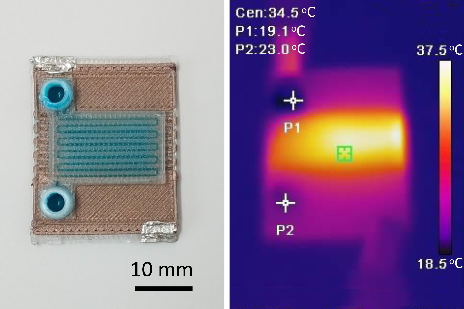
The tiny device could enable a user to rapidly create customized, low-cost objects on the go, like a fastener to repair a wobbly bicycle wheel or a component for a critical medical operation.

Turning up the heat on next-generation semiconductors

The scorching surface of Venus, where temperatures can climb to 480 degrees Celsius (hot enough to melt lead), is an inhospitable place for humans and machines alike. One reason scientists have not yet been able to send a rover to the planet’s surface is because silicon-based electronics can’t operate in such extreme temperatures for an extended period of time.

For high-temperature applications like Venus exploration, researchers have recently turned to gallium nitride, a unique material that can withstand temperatures of 500 degrees or more.

The material is already used in some terrestrial electronics, like phone chargers and cell phone towers, but scientists don’t have a good grasp of how gallium nitride devices would behave at temperatures beyond 300 degrees, which is the operational limit of conventional silicon electronics.

In a new paper published in Applied Physics Letterswhich is part of a multiyear research effort, a team of scientists from MIT and elsewhere sought to answer key questions about the material’s properties and performance at extremely high temperatures.  

They studied the impact of temperature on the ohmic contacts in a gallium nitride device. Ohmic contacts are key components that connect a semiconductor device with the outside world.

The researchers found that extreme temperatures didn’t cause significant degradation to the gallium nitride material or contacts. They were surprised to see that the contacts remained structurally intact even when held at 500 degrees Celsius for 48 hours.

Understanding how contacts perform at extreme temperatures is an important step toward the group’s next goal of developing high-performance transistors that could operate on the surface of Venus. Such transistors could also be used on Earth in electronics for applications like extracting geothermal energy or monitoring the inside of jet engines.

“Transistors are the heart of most modern electronics, but we didn’t want to jump straight to making a gallium nitride transistor because so much could go wrong. We first wanted to make sure the material and contacts could survive, and figure out how much they change as you increase the temperature. We’ll design our transistor from these basic material building blocks,” says John Niroula, an electrical engineering and computer science (EECS) graduate student and lead author of the paper.

His co-authors include Qingyun Xie PhD ’24; Mengyang Yuan PhD ’22; EECS graduate students Patrick K. Darmawi-Iskandar and Pradyot Yadav; Gillian K. Micale, a graduate student in the Department of Materials Science and Engineering; senior author Tomás Palacios, the Clarence J. LeBel Professor of EECS, director of the Microsystems Technology Laboratories, and a member of the Research Laboratory of Electronics; as well as collaborators Nitul S. Rajput of the Technology Innovation Institute of the United Arab Emirates; Siddharth Rajan of Ohio State University; Yuji Zhao of Rice University; and Nadim Chowdhury of Bangladesh University of Engineering and Technology.

Turning up the heat

While gallium nitride has recently attracted much attention, the material is still decades behind silicon when it comes to scientists’ understanding of how its properties change under different conditions. One such property is resistance, the flow of electrical current through a material.

A device’s overall resistance is inversely proportional to its size. But devices like semiconductors have contacts that connect them to other electronics. Contact resistance, which is caused by these electrical connections, remains fixed no matter the size of the device. Too much contact resistance can lead to higher power dissipation and slower operating frequencies for electronic circuits.

“Especially when you go to smaller dimensions, a device’s performance often ends up being limited by contact resistance. People have a relatively good understanding of contact resistance at room temperature, but no one has really studied what happens when you go all the way up to 500 degrees,” Niroula says.

For their study, the researchers used facilities at MIT.nano to build gallium nitride devices known as transfer length method structures, which are composed of a series of resistors. These devices enable them to measure the resistance of both the material and the contacts.

They added ohmic contacts to these devices using the two most common methods. The first involves depositing metal onto gallium nitride and heating it to 825 degrees Celsius for about 30 seconds, a process called annealing.

The second method involves removing chunks of gallium nitride and using a high-temperature technology to regrow highly doped gallium nitride in its place, a process led by Rajan and his team at Ohio State. The highly doped material contains extra electrons that can contribute to current conduction.

“The regrowth method typically leads to lower contact resistance at room temperature, but we wanted to see if these methods still work well at high temperatures,” Niroula says.

A comprehensive approach

They tested devices in two ways. Their collaborators at Rice University, led by Zhao, conducted short-term tests by placing devices on a hot chuck that reached 500 degrees Celsius and taking immediate resistance measurements.

At MIT, they conducted longer-term experiments by placing devices into a specialized furnace the group previously developed. They left devices inside for up to 72 hours to measure how resistance changes as a function of temperature and time.

Microscopy experts at MIT.nano (Aubrey N. Penn) and the Technology Innovation Institute (Nitul S. Rajput) used state-of-the-art transmission electron microscopes to see how such high temperatures affect gallium nitride and the ohmic contacts at the atomic level.

“We went in thinking the contacts or the gallium nitride material itself would degrade significantly, but we found the opposite. Contacts made with both methods seemed to be remarkably stable,” says Niroula.

While it is difficult to measure resistance at such high temperatures, their results indicate that contact resistance seems to remain constant even at temperatures of 500 degrees, for around 48 hours. And just like at room temperature, the regrowth process led to better performance.

The material did start to degrade after being in the furnace for 48 hours, but the researchers are already working to boost long-term performance. One strategy involves adding protective insulators to keep the material from being directly exposed to the high-temperature environment.

Moving forward, the researchers plan to use what they learned in these experiments to develop high-temperature gallium nitride transistors.

“In our group, we focus on innovative, device-level research to advance the frontiers of microelectronics, while adopting a systematic approach across the hierarchy, from the material level to the circuit level. Here, we have gone all the way down to the material level to understand things in depth. In other words, we have translated device-level advancements to circuit-level impact for high-temperature electronics, through design, modeling and complex fabrication. We are also immensely fortunate to have forged close partnerships with our longtime collaborators in this journey,” Xie says.

This work was funded, in part, by the U.S. Air Force Office of Scientific Research, Lockheed Martin Corporation, the Semiconductor Research Corporation through the U.S. Defense Advanced Research Projects Agency, the U.S. Department of Energy, Intel Corporation, and the Bangladesh University of Engineering and Technology.

Fabrication and microscopy were conducted at MIT.nano, the Semiconductor Epitaxy and Analysis Laboratory at Ohio State University, the Center for Advanced Materials Characterization at the University of Oregon, and the Technology Innovation Institute of the United Arab Emirates.

© Image: MIT News; iStock

Researchers studied how temperatures up to 500 degrees Celsius would affect electronic devices made from gallium nitride, a key step in their multiyear research effort to develop electronics that can operate in extremely hot environments, like the surface of Venus.

Researchers harness 2D magnetic materials for energy-efficient computing

Experimental computer memories and processors built from magnetic materials use far less energy than traditional silicon-based devices. Two-dimensional magnetic materials, composed of layers that are only a few atoms thick, have incredible properties that could allow magnetic-based devices to achieve unprecedented speed, efficiency, and scalability.

While many hurdles must be overcome until these so-called van der Waals magnetic materials can be integrated into functioning computers, MIT researchers took an important step in this direction by demonstrating precise control of a van der Waals magnet at room temperature.

This is key, since magnets composed of atomically thin van der Waals materials can typically only be controlled at extremely cold temperatures, making them difficult to deploy outside a laboratory.

The researchers used pulses of electrical current to switch the direction of the device’s magnetization at room temperature. Magnetic switching can be used in computation, the same way a transistor switches between open and closed to represent 0s and 1s in binary code, or in computer memory, where switching enables data storage.

The team fired bursts of electrons at a magnet made of a new material that can sustain its magnetism at higher temperatures. The experiment leveraged a fundamental property of electrons known as spin, which makes the electrons behave like tiny magnets. By manipulating the spin of electrons that strike the device, the researchers can switch its magnetization.

“The heterostructure device we have developed requires an order of magnitude lower electrical current to switch the van der Waals magnet, compared to that required for bulk magnetic devices,” says Deblina Sarkar, the AT&T Career Development Assistant Professor in the MIT Media Lab and Center for Neurobiological Engineering, head of the Nano-Cybernetic Biotrek Lab, and the senior author of a paper on this technique. “Our device is also more energy efficient than other van der Waals magnets that are unable to switch at room temperature.”

In the future, such a magnet could be used to build faster computers that consume less electricity. It could also enable magnetic computer memories that are nonvolatile, which means they don’t leak information when powered off, or processors that make complex AI algorithms more energy-efficient.

“There is a lot of inertia around trying to improve materials that worked well in the past. But we have shown that if you make radical changes, starting by rethinking the materials you are using, you can potentially get much better solutions,” says Shivam Kajale, a graduate student in Sarkar’s lab and co-lead author of the paper.

Kajale and Sarkar are joined on the paper by co-lead author Thanh Nguyen, a graduate student in the Department of Nuclear Science and Engineering (NSE); Corson Chao, a graduate student in the Department of Materials Science and Engineering (DSME); David Bono, a DSME research scientist; Artittaya Boonkird, an NSE graduate student; and Mingda Li, associate professor of nuclear science and engineering. The research appears this week in Nature Communications.

An atomically thin advantage

Methods to fabricate tiny computer chips in a clean room from bulk materials like silicon can hamper devices. For instance, the layers of material may be barely 1 nanometer thick, so minuscule rough spots on the surface can be severe enough to degrade performance.

By contrast, van der Waals magnetic materials are intrinsically layered and structured in such a way that the surface remains perfectly smooth, even as researchers peel off layers to make thinner devices. In addition, atoms in one layer won’t leak into other layers, enabling the materials to retain their unique properties when stacked in devices.

“In terms of scaling and making these magnetic devices competitive for commercial applications, van der Waals materials are the way to go,” Kajale says.

But there’s a catch. This new class of magnetic materials have typically only been operated at temperatures below 60 kelvins (-351 degrees Fahrenheit). To build a magnetic computer processor or memory, researchers need to use electrical current to operate the magnet at room temperature.

To achieve this, the team focused on an emerging material called iron gallium telluride. This atomically thin material has all the properties needed for effective room temperature magnetism and doesn’t contain rare earth elements, which are undesirable because extracting them is especially destructive to the environment.

Nguyen carefully grew bulk crystals of this 2D material using a special technique. Then, Kajale fabricated a two-layer magnetic device using nanoscale flakes of iron gallium telluride underneath a six-nanometer layer of platinum.

Tiny device in hand, they used an intrinsic property of electrons known as spin to switch its magnetization at room temperature.

Electron ping-pong

While electrons don’t technically “spin” like a top, they do possess the same kind of angular momentum. That spin has a direction, either up or down. The researchers can leverage a property known as spin-orbit coupling to control the spins of electrons they fire at the magnet.

The same way momentum is transferred when one ball hits another, electrons will transfer their “spin momentum” to the 2D magnetic material when they strike it. Depending on the direction of their spins, that momentum transfer can reverse the magnetization.

In a sense, this transfer rotates the magnetization from up to down (or vice-versa), so it is called a “torque,” as in spin-orbit torque switching. Applying a negative electric pulse causes the magnetization to go downward, while a positive pulse causes it to go upward.

The researchers can do this switching at room temperature for two reasons: the special properties of iron gallium telluride and the fact that their technique uses small amounts of electrical current. Pumping too much current into the device would cause it to overheat and demagnetize.

The team faced many challenges over the two years it took to achieve this milestone, Kajale says. Finding the right magnetic material was only half the battle. Since iron gallium telluride oxidizes quickly, fabrication must be done inside a glovebox filled with nitrogen.

“The device is only exposed to air for 10 or 15 seconds, but even after that I have to do a step where I polish it to remove any oxide,” he says.

Now that they have demonstrated room-temperature switching and greater energy efficiency, the researchers plan to keep pushing the performance of magnetic van der Waals materials.

“Our next milestone is to achieve switching without the need for any external magnetic fields. Our aim is to enhance our technology and scale up to bring the versatility of van der Waals magnet to commercial applications,” Sarkar says.

This work was carried out, in part, using the facilities at MIT.Nano and the Harvard University Center for Nanoscale Systems.

© Image: Courtesy of the researchers

This illustration shows electric current being pumped into platinum (the bottom slab), which results in the creation of an electron spin current that switches the magnetic state of the 2D ferromagnet on top. The colored spheres represent the atoms in the 2D material.

Technique could improve the sensitivity of quantum sensing devices

In quantum sensing, atomic-scale quantum systems are used to measure electromagnetic fields, as well as properties like rotation, acceleration, and distance, far more precisely than classical sensors can. The technology could enable devices that image the brain with unprecedented detail, for example, or air traffic control systems with precise positioning accuracy.

As many real-world quantum sensing devices are emerging, one promising direction is the use of microscopic defects inside diamonds to create “qubits” that can be used for quantum sensing. Qubits are the building blocks of quantum devices.

Researchers at MIT and elsewhere have developed a technique that enables them to identify and control a greater number of these microscopic defects. This could help them build a larger system of qubits that can perform quantum sensing with greater sensitivity.

Their method builds off a central defect inside a diamond, known as a nitrogen-vacancy (NV) center, which scientists can detect and excite using laser light and then control with microwave pulses. This new approach uses a specific protocol of microwave pulses to identify and extend that control to additional defects that can’t be seen with a laser, which are called dark spins.

The researchers seek to control larger numbers of dark spins by locating them through a network of connected spins. Starting from this central NV spin, the researchers build this chain by coupling the NV spin to a nearby dark spin, and then use this dark spin as a probe to find and control a more distant spin which can’t be sensed by the NV directly. The process can be repeated on these more distant spins to control longer chains.

“One lesson I learned from this work is that searching in the dark may be quite discouraging when you don’t see results, but we were able to take this risk. It is possible, with some courage, to search in places that people haven’t looked before and find potentially more advantageous qubits,” says Alex Ungar, a PhD student in electrical engineering and computer science and a member of the Quantum Engineering Group at MIT, who is lead author of a paper on this technique, which is published today in PRX Quantum.

His co-authors include his advisor and corresponding author, Paola Cappellaro, the Ford Professor of Engineering in the Department of Nuclear Science and Engineering and professor of physics; as well as Alexandre Cooper, a senior research scientist at the University of Waterloo’s Institute for Quantum Computing; and Won Kyu Calvin Sun, a former researcher in Cappellaro’s group who is now a postdoc at the University of Illinois at Urbana-Champaign.

Diamond defects

To create NV centers, scientists implant nitrogen into a sample of diamond.

But introducing nitrogen into the diamond creates other types of atomic defects in the surrounding environment. Some of these defects, including the NV center, can host what are known as electronic spins, which originate from the valence electrons around the site of the defect. Valence electrons are those in the outermost shell of an atom. A defect’s interaction with an external magnetic field can be used to form a qubit.

Researchers can harness these electronic spins from neighboring defects to create more qubits around a single NV center. This larger collection of qubits is known as a quantum register. Having a larger quantum register boosts the performance of a quantum sensor.

Some of these electronic spin defects are connected to the NV center through magnetic interaction. In past work, researchers used this interaction to identify and control nearby spins. However, this approach is limited because the NV center is only stable for a short amount of time, a principle called coherence. It can only be used to control the few spins that can be reached within this coherence limit.

In this new paper, the researchers use an electronic spin defect that is near the NV center as a probe to find and control an additional spin, creating a chain of three qubits.

They use a technique known as spin echo double resonance (SEDOR), which involves a series of microwave pulses that decouple an NV center from all electronic spins that are interacting with it. Then, they selectively apply another microwave pulse to pair the NV center with one nearby spin.

Unlike the NV, these neighboring dark spins can’t be excited, or polarized, with laser light. This polarization is a required step to control them with microwaves.

Once the researchers find and characterize a first-layer spin, they can transfer the NV’s polarization to this first-layer spin through the magnetic interaction by applying microwaves to both spins simultaneously. Then once the first-layer spin is polarized, they repeat the SEDOR process on the first-layer spin, using it as a probe to identify a second-layer spin that is interacting with it.

Controlling a chain of dark spins

This repeated SEDOR process allows the researchers to detect and characterize a new, distinct defect located outside the coherence limit of the NV center. To control this more distant spin, they carefully apply a specific series of microwave pulses that enable them to transfer the polarization from the NV center along the chain to this second-layer spin.

“This is setting the stage for building larger quantum registers to higher-layer spins or longer spin chains, and also showing that we can find these new defects that weren’t discovered before by scaling up this technique,” Ungar says.

To control a spin, the microwave pulses must be very close to the resonance frequency of that spin. Tiny drifts in the experimental setup, due to temperature or vibrations, can throw off the microwave pulses.

The researchers were able to optimize their protocol for sending precise microwave pulses, which enabled them to effectively identify and control second-layer spins, Ungar says.

“We are searching for something in the unknown, but at the same time, the environment might not be stable, so you don’t know if what you are finding is just noise. Once you start seeing promising things, you can put all your best effort in that one direction. But before you arrive there, it is a leap of faith,” Cappellaro says.

While they were able to effectively demonstrate a three-spin chain, the researchers estimate they could scale their method to a fifth layer using their current protocol, which could provide access to hundreds of potential qubits. With further optimization, they may be able to scale up to more than 10 layers.

In the future, they plan to continue enhancing their technique to efficiently characterize and probe other electronic spins in the environment and explore different types of defects that could be used to form qubits.

This research is supported, in part, by the U.S. National Science Foundation and the Canada First Research Excellence Fund.

© Image: Courtesy of the researchers

Researchers use microscopic defects inside a diamond to build a chain of three qubits (pictured as small circles with arrows) that they can use for quantum sensing. They start from a central defect, couple it with a nearby defect, and then use this second defect to find and control a third defect.

Closing the design-to-manufacturing gap for optical devices

Photolithography involves manipulating light to precisely etch features onto a surface, and is commonly used to fabricate computer chips and optical devices like lenses. But tiny deviations during the manufacturing process often cause these devices to fall short of their designers’ intentions.

To help close this design-to-manufacturing gap, researchers from MIT and the Chinese University of Hong Kong used machine learning to build a digital simulator that mimics a specific photolithography manufacturing process. Their technique utilizes real data gathered from the photolithography system, so it can more accurately model how the system would fabricate a design.

The researchers integrate this simulator into a design framework, along with another digital simulator that emulates the performance of the fabricated device in downstream tasks, such as producing images with computational cameras. These connected simulators enable a user to produce an optical device that better matches its design and reaches the best task performance.

This technique could help scientists and engineers create more accurate and efficient optical devices for applications like mobile cameras, augmented reality, medical imaging, entertainment, and telecommunications. And because the pipeline of learning the digital simulator utilizes real-world data, it can be applied to a wide range of photolithography systems.

“This idea sounds simple, but the reasons people haven’t tried this before are that real data can be expensive and there are no precedents for how to effectively coordinate the software and hardware to build a high-fidelity dataset,” says Cheng Zheng, a mechanical engineering graduate student who is co-lead author of an open-access paper describing the work. “We have taken risks and done extensive exploration, for example, developing and trying characterization tools and data-exploration strategies, to determine a working scheme. The result is surprisingly good, showing that real data work much more efficiently and precisely than data generated by simulators composed of analytical equations. Even though it can be expensive and one can feel clueless at the beginning, it is worth doing.”

Zheng wrote the paper with co-lead author Guangyuan Zhao, a graduate student at the Chinese University of Hong Kong; and her advisor, Peter T. So, a professor of mechanical engineering and biological engineering at MIT. The research will be presented at the SIGGRAPH Asia Conference.

Printing with light

Photolithography involves projecting a pattern of light onto a surface, which causes a chemical reaction that etches features into the substrate. However, the fabricated device ends up with a slightly different pattern because of miniscule deviations in the light’s diffraction and tiny variations in the chemical reaction.

Because photolithography is complex and hard to model, many existing design approaches rely on equations derived from physics. These general equations give some sense of the fabrication process but can’t capture all deviations specific to a photolithography system. This can cause devices to underperform in the real world.

For their technique, which they call neural lithography, the MIT researchers build their photolithography simulator using physics-based equations as a base, and then incorporate a neural network trained on real, experimental data from a user’s photolithography system. This neural network, a type of machine-learning model loosely based on the human brain, learns to compensate for many of the system’s specific deviations.

The researchers gather data for their method by generating many designs that cover a wide range of feature sizes and shapes, which they fabricate using the photolithography system. They measure the final structures and compare them with design specifications, pairing those data and using them to train a neural network for their digital simulator.

“The performance of learned simulators depends on the data fed in, and data artificially generated from equations can’t cover real-world deviations, which is why it is important to have real-world data,” Zheng says.

Dual simulators

The digital lithography simulator consists of two separate components: an optics model that captures how light is projected on the surface of the device, and a resist model that shows how the photochemical reaction occurs to produce features on the surface.

In a downstream task, they connect this learned photolithography simulator to a physics-based simulator that predicts how the fabricated device will perform on this task, such as how a diffractive lens will diffract the light that strikes it.

The user specifies the outcomes they want a device to achieve. Then these two simulators work together within a larger framework that shows the user how to make a design that will reach those performance goals.

“With our simulator, the fabricated object can get the best possible performance on a downstream task, like the computational cameras, a promising technology to make future cameras miniaturized and more powerful. We show that, even if you use post-calibration to try and get a better result, it will still not be as good as having our photolithography model in the loop,” Zhao adds.

They tested this technique by fabricating a holographic element that generates a butterfly image when light shines on it. When compared to devices designed using other techniques, their holographic element produced a near-perfect butterfly that more closely matched the design. They also produced a multilevel diffraction lens, which had better image quality than other devices.

In the future, the researchers want to enhance their algorithms to model more complicated devices, and also test the system using consumer cameras. In addition, they want to expand their approach so it can be used with different types of photolithography systems, such as systems that use deep or extreme ultraviolet light.

This research is supported, in part, by the U.S. National Institutes of Health, Fujikura Limited, and the Hong Kong Innovation and Technology Fund.

The work was carried out, in part, using MIT.nano’s facilities.

© Image: MIT News; iStock

Researchers from MIT and elsewhere created an AI technique that learns to simulate a photolithography system, capturing the tiny deviations the system introduces during manufacturing. This method could enable a researcher to fabricate optical devices that more closely match their design specifications, boosting the accuracy and efficiency of electronics.

Scientists 3D print self-heating microfluidic devices

MIT researchers have used 3D printing to produce self-heating microfluidic devices, demonstrating a technique which could someday be used to rapidly create cheap, yet accurate, tools to detect a host of diseases.

Microfluidics, miniaturized machines that manipulate fluids and facilitate chemical reactions, can be used to detect disease in tiny samples of blood or fluids. At-home test kits for Covid-19, for example, incorporate a simple type of microfluidic.

But many microfluidic applications require chemical reactions that must be performed at specific temperatures. These more complex microfluidic devices, which are typically manufactured in a clean room, are outfitted with heating elements made from gold or platinum using a complicated and expensive fabrication process that is difficult to scale up.

Instead, the MIT team used multimaterial 3D printing to create self-heating microfluidic devices with built-in heating elements, through a single, inexpensive manufacturing process. They generated devices that can heat fluid to a specific temperature as it flows through microscopic channels inside the tiny machine.

Their technique is customizable, so an engineer could create a microfluidic that heats fluid to a certain temperature or given heating profile within a specific area of the device. The low-cost fabrication process requires about $2 of materials to generate a ready-to-use microfluidic.

The process could be especially useful in creating self-heating microfluidics for remote regions of developing countries where clinicians may not have access to the expensive lab equipment required for many diagnostic procedures.

“Clean rooms in particular, where you would usually make these devices, are incredibly expensive to build and to run. But we can make very capable self-heating microfluidic devices using additive manufacturing, and they can be made a lot faster and cheaper than with these traditional methods. This is really a way to democratize this technology,” says Luis Fernando Velásquez-García, a principal scientist in MIT’s Microsystems Technology Laboratories (MTL) and senior author of a paper describing the fabrication technique.

He is joined on the paper by lead author Jorge Cañada Pérez-Sala, an electrical engineering and computer science graduate student. The research will be presented at the PowerMEMS Conference this month.

An insulator becomes conductive

This new fabrication process utilizes a technique called multimaterial extrusion 3D printing, in which several materials can be squirted through the printer’s many nozzles to build a device layer by layer. The process is monolithic, which means the entire device can be produced in one step on the 3D printer, without the need for any post-assembly.

To create self-heating microfluidics, the researchers used two materials — a biodegradable polymer known as polylactic acid (PLA) that is commonly used in 3D printing, and a modified version of PLA.

The modified PLA has mixed copper nanoparticles into the polymer, which converts this insulating material into an electrical conductor, Velásquez-García explains. When electrical current is fed into a resistor composed of this copper-doped PLA, energy is dissipated as heat.

“It is amazing when you think about it because the PLA material is a dielectric, but when you put in these nanoparticle impurities, it completely changes the physical properties. This is something we don’t fully understand yet, but it happens and it is repeatable,” he says.

Using a multimaterial 3D printer, the researchers fabricate a heating resistor from the copper-doped PLA and then print the microfluidic device, with microscopic channels through which fluid can flow, directly on top in one printing step. Because the components are made from the same base material, they have similar printing temperatures and are compatible.

Heat dissipated from the resistor will warm fluid flowing through the channels in the microfluidic.

In addition to the resistor and microfluidic, they use the printer to add a thin, continuous layer of PLA that is sandwiched between them. It is especially challenging to manufacture this layer because it must be thin enough so heat can transfer from the resistor to the microfluidic, but not so thin that fluid could leak into the resistor.

The resulting machine is about the size of a U.S. quarter and can be produced in a matter of minutes. Channels about 500 micrometers wide and 400 micrometers tall are threaded through the microfluidic to carry fluid and facilitate chemical reactions.

Importantly, the PLA material is translucent, so fluid in the device remains visible. Many processes rely on visualization or the use of light to infer what is happening during chemical reactions, Velásquez-García explains.

Customizable chemical reactors

The researchers used this one-step manufacturing process to generate a prototype that could heat fluid by 4 degrees Celsius as it flowed between the input and the output. This customizable technique could enable them to make devices which would heat fluids in certain patterns or along specific gradients.

“You can use these two materials to create chemical reactors that do exactly what you want. We can set up a particular heating profile while still having all the capabilities of the microfluidic,” he says.

However, one limitation comes from the fact that PLA can only be heated to about 50 degrees Celsius before it starts to degrade. Many chemical reactions, such as those used for polymerase chain reaction (PCR) tests, require temperatures of 90 degrees or higher. And to precisely control the temperature of the device, researchers would need to integrate a third material that enables temperature sensing.

In addition to tackling these limitations in future work, Velásquez-García wants to print magnets directly into the microfluidic device. These magnets could enable chemical reactions that require particles to be sorted or aligned.

At the same time, he and his colleagues are exploring the use of other materials that could reach higher temperatures. They are also studying PLA to better understand why it becomes conductive when certain impurities are added to the polymer.

“If we can understand the mechanism that is related to the electrical conductivity of PLA, that would greatly enhance the capability of these devices, but it is going to be a lot harder to solve than some other engineering problems,” he adds.

“In Japanese culture, it’s often said that beauty lies in simplicity. This sentiment is echoed by the work of Cañada and Velasquez-Garcia. Their proposed monolithically 3D-printed microfluidic systems embody simplicity and beauty, offering a wide array of potential derivations and applications that we foresee in the future,” says Norihisa Miki, a professor of mechanical engineering at Keio University in Tokyo, who was not involved with this work.

“Being able to directly print microfluidic chips with fluidic channels and electrical features at the same time opens up very exiting applications when processing biological samples, such as to amplify biomarkers or to actuate and mix liquids. Also, due to the fact that PLA degrades over time, one can even think of implantable applications where the chips dissolve and resorb over time,” adds Niclas Roxhed, an associate professor at Sweden’s KTH Royal Institute of Technology, who was not involved with this study.

This research was funded, in part, by the Empiriko Corporation and a fellowship from La Caixa Foundation.

© Image: Courtesy of the researchers

MIT researchers developed a fabrication process to produce self-heating microfluidic devices in one step using a multi-material 3D printer. Pictured is an example of one of the devices.

Researchers safely integrate fragile 2D materials into devices

Two-dimensional materials, which are only a few atoms thick, can exhibit some incredible properties, such as the ability to carry electric charge extremely efficiently, which could boost the performance of next-generation electronic devices.

But integrating 2D materials into devices and systems like computer chips is notoriously difficult. These ultrathin structures can be damaged by conventional fabrication techniques, which often rely on the use of chemicals, high temperatures, or destructive processes like etching.

To overcome this challenge, researchers from MIT and elsewhere have developed a new technique to integrate 2D materials into devices in a single step while keeping the surfaces of the materials and the resulting interfaces pristine and free from defects.

Their method relies on engineering surface forces available at the nanoscale to allow the 2D material to be physically stacked onto other prebuilt device layers. Because the 2D material remains undamaged, the researchers can take full advantage of its unique optical and electrical properties.

They used this approach to fabricate arrays of 2D transistors that achieved new functionalities compared to devices produced using conventional fabrication techniques. Their method, which is versatile enough to be used with many materials, could have diverse applications in high-performance computing, sensing, and flexible electronics.

Core to unlocking these new functionalities is the ability to form clean interfaces, held together by special forces that exist between all matter, called van der Waals forces.

However, such van der Waals integration of materials into fully functional devices is not always easy, says Farnaz Niroui, assistant professor of electrical engineering and computer science (EECS), a member of the Research Laboratory of Electronics (RLE), and senior author of a new paper describing the work.

“Van der Waals integration has a fundamental limit,” she explains. “Since these forces depend on the intrinsic properties of the materials, they cannot be readily tuned. As a result, there are some materials that cannot be directly integrated with each other using their van der Waals interactions alone. We have come up with a platform to address this limit to help make van der Waals integration more versatile, to promote the development of 2D-materials-based devices with new and improved functionalities.”

Niroui wrote the paper with lead author Peter Satterthwaite, an electrical engineering and computer science graduate student; Jing Kong, professor of EECS and a member of RLE; and others at MIT, Boston University, National Tsing Hua University in Taiwan, the National Science and Technology Council of Taiwan, and National Cheng Kung University in Taiwan. The research is published today in Nature Electronics.  

Advantageous attraction

Making complex systems such as a computer chip with conventional fabrication techniques can get messy. Typically, a rigid material like silicon is chiseled down to the nanoscale, then interfaced with other components like metal electrodes and insulating layers to form an active device. Such processing can cause damage to the materials.

Recently, researchers have focused on building devices and systems from the bottom up, using 2D materials and a process that requires sequential physical stacking. In this approach, rather than using chemical glues or high temperatures to bond a fragile 2D material to a conventional surface like silicon, researchers leverage van der Waals forces to physically integrate a layer of 2D material onto a device.

Van der Waals forces are natural forces of attraction that exist between all matter. For example, a gecko’s feet can stick to the wall temporarily due to van der Waals forces. Though all materials exhibit a van der Waals interaction, depending on the material, the forces are not always strong enough to hold them together. For instance, a popular semiconducting 2D material known as molybdenum disulfide will stick to gold, a metal, but won’t directly transfer to insulators like silicon dioxide by just coming into physical contact with that surface.

However, heterostructures made by integrating semiconductor and insulating layers are key building blocks of an electronic device. Previously, this integration has been enabled by bonding the 2D material to an intermediate layer like gold, then using this intermediate layer to transfer the 2D material onto the insulator, before removing the intermediate layer using chemicals or high temperatures.

Instead of using this sacrificial layer, the MIT researchers embed the low-adhesion insulator in a high-adhesion matrix. This adhesive matrix is what makes the 2D material stick to the embedded low-adhesion surface, providing the forces needed to create a van der Waals interface between the 2D material and the insulator.

Making the matrix

To make electronic devices, they form a hybrid surface of metals and insulators on a carrier substrate. This surface is then peeled off and flipped over to reveal a completely smooth top surface that contains the building blocks of the desired device.

This smoothness is important, since gaps between the surface and 2D material can hamper van der Waals interactions. Then, the researchers prepare the 2D material separately, in a completely clean environment, and bring it into direct contact with the prepared device stack.

“Once the hybrid surface is brought into contact with the 2D layer, without needing any high-temperatures, solvents, or sacrificial layers, it can pick up the 2D layer and integrate it with the surface. This way, we are allowing a van der Waals integration that would be traditionally forbidden, but now is possible and allows formation of fully functioning devices in a single step,” Satterthwaite explains.

This single-step process keeps the 2D material interface completely clean, which enables the material to reach its fundamental limits of performance without being held back by defects or contamination.

And because the surfaces also remain pristine, researchers can engineer the surface of the 2D material to form features or connections to other components. For example, they used this technique to create p-type transistors, which are generally challenging to make with 2D materials. Their transistors have improved on previous studies, and can provide a platform toward studying and achieving the performance needed for practical electronics.

Their approach can be done at scale to make larger arrays of devices. The adhesive matrix technique can also be used with a range of materials, and even with other forces to enhance the versatility of this platform. For instance, the researchers integrated graphene onto a device, forming the desired van der Waals interfaces using a matrix made with a polymer. In this case, adhesion relies on chemical interactions rather than van der Waals forces alone.

In the future, the researchers want to build on this platform to enable integration of a diverse library of 2D materials to study their intrinsic properties without the influence of processing damage, and develop new device platforms that leverage these superior functionalities.  

This research is funded, in part, by the U.S. National Science Foundation, the U.S. Department of Energy, the BUnano Cross-Disciplinary Fellowship at Boston University, and the U.S. Army Research Office. The fabrication and characterization procedures were carried out, largely, in the MIT.nano shared facilities.

© Image: Courtesy of Sampson Wilcox/Research Laboratory of Electronics

This artist’s rendition shows a new integration platform developed by MIT researchers. By engineering surface forces, they can directly integrate 2D materials into devices in a single contact-and-release step.

Researchers harness 2D magnetic materials for energy-efficient computing

Experimental computer memories and processors built from magnetic materials use far less energy than traditional silicon-based devices. Two-dimensional magnetic materials, composed of layers that are only a few atoms thick, have incredible properties that could allow magnetic-based devices to achieve unprecedented speed, efficiency, and scalability.

While many hurdles must be overcome until these so-called van der Waals magnetic materials can be integrated into functioning computers, MIT researchers took an important step in this direction by demonstrating precise control of a van der Waals magnet at room temperature.

This is key, since magnets composed of atomically thin van der Waals materials can typically only be controlled at extremely cold temperatures, making them difficult to deploy outside a laboratory.

The researchers used pulses of electrical current to switch the direction of the device’s magnetization at room temperature. Magnetic switching can be used in computation, the same way a transistor switches between open and closed to represent 0s and 1s in binary code, or in computer memory, where switching enables data storage.

The team fired bursts of electrons at a magnet made of a new material that can sustain its magnetism at higher temperatures. The experiment leveraged a fundamental property of electrons known as spin, which makes the electrons behave like tiny magnets. By manipulating the spin of electrons that strike the device, the researchers can switch its magnetization.

“The heterostructure device we have developed requires an order of magnitude lower electrical current to switch the van der Waals magnet, compared to that required for bulk magnetic devices,” says Deblina Sarkar, the AT&T Career Development Assistant Professor in the MIT Media Lab and Center for Neurobiological Engineering, head of the Nano-Cybernetic Biotrek Lab, and the senior author of a paper on this technique. “Our device is also more energy efficient than other van der Waals magnets that are unable to switch at room temperature.”

In the future, such a magnet could be used to build faster computers that consume less electricity. It could also enable magnetic computer memories that are nonvolatile, which means they don’t leak information when powered off, or processors that make complex AI algorithms more energy-efficient.

“There is a lot of inertia around trying to improve materials that worked well in the past. But we have shown that if you make radical changes, starting by rethinking the materials you are using, you can potentially get much better solutions,” says Shivam Kajale, a graduate student in Sarkar’s lab and co-lead author of the paper.

Kajale and Sarkar are joined on the paper by co-lead author Thanh Nguyen, a graduate student in the Department of Nuclear Science and Engineering (NSE); Corson Chao, a graduate student in the Department of Materials Science and Engineering (DSME); David Bono, a DSME research scientist; Artittaya Boonkird, an NSE graduate student; and Mingda Li, associate professor of nuclear science and engineering. The research appears this week in Nature Communications.

An atomically thin advantage

Methods to fabricate tiny computer chips in a clean room from bulk materials like silicon can hamper devices. For instance, the layers of material may be barely 1 nanometer thick, so minuscule rough spots on the surface can be severe enough to degrade performance.

By contrast, van der Waals magnetic materials are intrinsically layered and structured in such a way that the surface remains perfectly smooth, even as researchers peel off layers to make thinner devices. In addition, atoms in one layer won’t leak into other layers, enabling the materials to retain their unique properties when stacked in devices.

“In terms of scaling and making these magnetic devices competitive for commercial applications, van der Waals materials are the way to go,” Kajale says.

But there’s a catch. This new class of magnetic materials have typically only been operated at temperatures below 60 kelvins (-351 degrees Fahrenheit). To build a magnetic computer processor or memory, researchers need to use electrical current to operate the magnet at room temperature.

To achieve this, the team focused on an emerging material called iron gallium telluride. This atomically thin material has all the properties needed for effective room temperature magnetism and doesn’t contain rare earth elements, which are undesirable because extracting them is especially destructive to the environment.

Nguyen carefully grew bulk crystals of this 2D material using a special technique. Then, Kajale fabricated a two-layer magnetic device using nanoscale flakes of iron gallium telluride underneath a six-nanometer layer of platinum.

Tiny device in hand, they used an intrinsic property of electrons known as spin to switch its magnetization at room temperature.

Electron ping-pong

While electrons don’t technically “spin” like a top, they do possess the same kind of angular momentum. That spin has a direction, either up or down. The researchers can leverage a property known as spin-orbit coupling to control the spins of electrons they fire at the magnet.

The same way momentum is transferred when one ball hits another, electrons will transfer their “spin momentum” to the 2D magnetic material when they strike it. Depending on the direction of their spins, that momentum transfer can reverse the magnetization.

In a sense, this transfer rotates the magnetization from up to down (or vice-versa), so it is called a “torque,” as in spin-orbit torque switching. Applying a negative electric pulse causes the magnetization to go downward, while a positive pulse causes it to go upward.

The researchers can do this switching at room temperature for two reasons: the special properties of iron gallium telluride and the fact that their technique uses small amounts of electrical current. Pumping too much current into the device would cause it to overheat and demagnetize.

The team faced many challenges over the two years it took to achieve this milestone, Kajale says. Finding the right magnetic material was only half the battle. Since iron gallium telluride oxidizes quickly, fabrication must be done inside a glovebox filled with nitrogen.

“The device is only exposed to air for 10 or 15 seconds, but even after that I have to do a step where I polish it to remove any oxide,” he says.

Now that they have demonstrated room-temperature switching and greater energy efficiency, the researchers plan to keep pushing the performance of magnetic van der Waals materials.

“Our next milestone is to achieve switching without the need for any external magnetic fields. Our aim is to enhance our technology and scale up to bring the versatility of van der Waals magnet to commercial applications,” Sarkar says.

This work was carried out, in part, using the facilities at MIT.Nano and the Harvard University Center for Nanoscale Systems.

© Image: Courtesy of the researchers

This illustration shows electric current being pumped into platinum (the bottom slab), which results in the creation of an electron spin current that switches the magnetic state of the 2D ferromagnet on top. The colored spheres represent the atoms in the 2D material.
❌