FreshRSS

Zobrazení pro čtení

Jsou dostupné nové články, klikněte pro obnovení stránky.

Seizing solar’s bright future

Consider the dizzying ascent of solar energy in the United States: In the past decade, solar capacity increased nearly 900 percent, with electricity production eight times greater in 2023 than in 2014. The jump from 2022 to 2023 alone was 51 percent, with a record 32 gigawatts (GW) of solar installations coming online. In the past four years, more solar has been added to the grid than any other form of generation. Installed solar now tops 179 GW, enough to power nearly 33 million homes. The U.S. Department of Energy (DOE) is so bullish on the sun that its decarbonization plans envision solar satisfying 45 percent of the nation’s electricity demands by 2050.

But the continued rapid expansion of solar requires advances in technology, notably to improve the efficiency and durability of solar photovoltaic (PV) materials and manufacturing. That’s where Optigon, a three-year-old MIT spinout company, comes in.

“Our goal is to build tools for research and industry that can accelerate the energy transition,” says Dane deQuilettes, the company’s co-founder and chief science officer. “The technology we have developed for solar will enable measurements and analysis of materials as they are being made both in lab and on the manufacturing line, dramatically speeding up the optimization of PV.”

With roots in MIT’s vibrant solar research community, Optigon is poised for a 2024 rollout of technology it believes will drastically pick up the pace of solar power and other clean energy projects.

Beyond silicon

Silicon, the material mainstay of most PV, is limited by the laws of physics in the efficiencies it can achieve converting photons from the sun into electrical energy. Silicon-based solar cells can theoretically reach power conversion levels of just 30 percent, and real-world efficiency levels hover in the low 20s. But beyond the physical limitations of silicon, there is another issue at play for many researchers and the solar industry in the United States and elsewhere: China dominates the silicon PV market, from supply chains to manufacturing.

Scientists are eagerly pursuing alternative materials, either for enhancing silicon’s solar conversion capacity or for replacing silicon altogether.

In the past decade, a family of crystal-structured semiconductors known as perovskites has risen to the fore as a next-generation PV material candidate. Perovskite devices lend themselves to a novel manufacturing process using printing technology that could circumvent the supply chain juggernaut China has built for silicon. Perovskite solar cells can be stacked on each other or layered atop silicon PV, to achieve higher conversion efficiencies. Because perovskite technology is flexible and lightweight, modules can be used on roofs and other structures that cannot support heavier silicon PV, lowering costs and enabling a wider range of building-integrated solar devices.

But these new materials require testing, both during R&D and then on assembly lines, where missing or defective optical, electrical, or dimensional properties in the nano-sized crystal structures can negatively impact the end product.

“The actual measurement and data analysis processes have been really, really slow, because you have to use a bunch of separate tools that are all very manual,” says Optigon co-founder and chief executive officer Anthony Troupe ’21. “We wanted to come up with tools for automating detection of a material’s properties, for determining whether it could make a good or bad solar cell, and then for optimizing it.”

“Our approach packed several non-contact, optical measurements using different types of light sources and detectors into a single system, which together provide a holistic, cross-sectional view of the material,” says Brandon Motes ’21, ME ’22, co-founder and chief technical officer.

“This breakthrough in achieving millisecond timescales for data collection and analysis means we can take research-quality tools and actually put them on a full production system, getting extremely detailed information about products being built at massive, gigawatt scale in real-time,” says Troupe.

This streamlined system takes measurements “in the snap of the fingers, unlike the traditional tools,” says Joseph Berry, director of the US Manufacturing of Advanced Perovskites Consortium and a senior research scientist at the National Renewable Energy Laboratory. “Optigon’s techniques are high precision and allow high throughput, which means they can be used in a lot of contexts where you want rapid feedback and the ability to develop materials very, very quickly.”

According to Berry, Optigon’s technology may give the solar industry not just better materials, but the ability to pump out high-quality PV products at a brisker clip than is currently possible. “If Optigon is successful in deploying their technology, then we can more rapidly develop the materials that we need, manufacturing with the requisite precision again and again,” he says. “This could lead to the next generation of PV modules at a much, much lower cost.”

Measuring makes the difference

With Small Business Innovation Research funding from DOE to commercialize its products and a grant from the Massachusetts Clean Energy Center, Optigon has settled into a space at the climate technology incubator Greentown Labs in Somerville, Massachusetts. Here, the team is preparing for this spring’s launch of its first commercial product, whose genesis lies in MIT’s GridEdge Solar Research Program.

Led by Vladimir Bulović, a professor of electrical engineering and the director of MIT.nano, the GridEdge program was established with funding from the Tata Trusts to develop lightweight, flexible, and inexpensive solar cells for distribution to rural communities around the globe. When deQuilettes joined the group in 2017 as a postdoc, he was tasked with directing the program and building the infrastructure to study and make perovskite solar modules.

“We were trying to understand once we made the material whether or not it was good,” he recalls. “There were no good commercial metrology [the science of measurements] tools for materials beyond silicon, so we started to build our own.” Recognizing the group’s need for greater expertise on the problem, especially in the areas of electrical, software, and mechanical engineering, deQuilettes put a call out for undergraduate researchers to help build metrology tools for new solar materials.

“Forty people inquired, but when I met Brandon and Anthony, something clicked; it was clear we had a complementary skill set,” says deQuilettes. “We started working together, with Anthony coming up with beautiful designs to integrate multiple measurements, and Brandon creating boards to control all of the hardware, including different types of lasers. We started filing multiple patents and that was when we saw it all coming together.”

“We knew from the start that metrology could vastly improve not just materials, but production yields,” says Troupe. Adds deQuilettes, “Our goal was getting to the highest performance orders of magnitude faster than it would ordinarily take, so we developed tools that would not just be useful for research labs but for manufacturing lines to give live feedback on quality.”

The device Optigon designed for industry is the size of a football, “with sensor packages crammed into a tiny form factor, taking measurements as material flows directly underneath,” says Motes. “We have also thought carefully about ways to make interaction with this tool as seamless and, dare I say, as enjoyable as possible, streaming data to both a dashboard an operator can watch and to a custom database.”

Photovoltaics is just the start

The company may have already found its market niche. “A research group paid us to use our in-house prototype because they have such a burning need to get these sorts of measurements,” says Troupe, and according to Motes, “Potential customers ask us if they can buy the system now.” deQuilettes says, “Our hope is that we become the de facto company for doing any sort of characterization metrology in the United States and beyond.”

Challenges lie ahead for Optigon: product launches, full-scale manufacturing, technical assistance, and sales. Greentown Labs offers support, as does MIT’s own rich community of solar researchers and entrepreneurs. But the founders are already thinking about next phases.

“We are not limiting ourselves to the photovoltaics area,” says deQuilettes. “We’re planning on working in other clean energy materials such as batteries and fuel cells.”

That’s because the team wants to make the maximum impact on the climate challenge. “We’ve thought a lot about the potential our tools will have on reducing carbon emissions, and we’ve done a really in-depth analysis looking at how our system can increase production yields of solar panels and other energy technologies, reducing materials and energy wasted in conventional optimization,” deQuilettes says. “If we look across all these sectors, we can expect to offset about 1,000 million metric tons of CO2 [carbon dioxide] per year in the not-too-distant future.”

The team has written scale into its business plan. “We want to be the key enabler for bringing these new energy technologies to market,” says Motes. “We envision being deployed on every manufacturing line making these types of materials. It’s our goal to walk around and know that if we see a solar panel deployed, there’s a pretty high likelihood that it will be one we measured at some point.”

© Photo: Natalie Hill/Greentown Labs


Optigon co-founders (from left to right) Brandon Motes, Dane deQuilettes, and Anthony Troupe stand with a benchtop version of the measurement tool they believe will help accelerate the pace of solar power and other clean energy products.

Seizing solar’s bright future

Consider the dizzying ascent of solar energy in the United States: In the past decade, solar capacity increased nearly 900 percent, with electricity production eight times greater in 2023 than in 2014. The jump from 2022 to 2023 alone was 51 percent, with a record 32 gigawatts (GW) of solar installations coming online. In the past four years, more solar has been added to the grid than any other form of generation. Installed solar now tops 179 GW, enough to power nearly 33 million homes. The U.S. Department of Energy (DOE) is so bullish on the sun that its decarbonization plans envision solar satisfying 45 percent of the nation’s electricity demands by 2050.

But the continued rapid expansion of solar requires advances in technology, notably to improve the efficiency and durability of solar photovoltaic (PV) materials and manufacturing. That’s where Optigon, a three-year-old MIT spinout company, comes in.

“Our goal is to build tools for research and industry that can accelerate the energy transition,” says Dane deQuilettes, the company’s co-founder and chief science officer. “The technology we have developed for solar will enable measurements and analysis of materials as they are being made both in lab and on the manufacturing line, dramatically speeding up the optimization of PV.”

With roots in MIT’s vibrant solar research community, Optigon is poised for a 2024 rollout of technology it believes will drastically pick up the pace of solar power and other clean energy projects.

Beyond silicon

Silicon, the material mainstay of most PV, is limited by the laws of physics in the efficiencies it can achieve converting photons from the sun into electrical energy. Silicon-based solar cells can theoretically reach power conversion levels of just 30 percent, and real-world efficiency levels hover in the low 20s. But beyond the physical limitations of silicon, there is another issue at play for many researchers and the solar industry in the United States and elsewhere: China dominates the silicon PV market, from supply chains to manufacturing.

Scientists are eagerly pursuing alternative materials, either for enhancing silicon’s solar conversion capacity or for replacing silicon altogether.

In the past decade, a family of crystal-structured semiconductors known as perovskites has risen to the fore as a next-generation PV material candidate. Perovskite devices lend themselves to a novel manufacturing process using printing technology that could circumvent the supply chain juggernaut China has built for silicon. Perovskite solar cells can be stacked on each other or layered atop silicon PV, to achieve higher conversion efficiencies. Because perovskite technology is flexible and lightweight, modules can be used on roofs and other structures that cannot support heavier silicon PV, lowering costs and enabling a wider range of building-integrated solar devices.

But these new materials require testing, both during R&D and then on assembly lines, where missing or defective optical, electrical, or dimensional properties in the nano-sized crystal structures can negatively impact the end product.

“The actual measurement and data analysis processes have been really, really slow, because you have to use a bunch of separate tools that are all very manual,” says Optigon co-founder and chief executive officer Anthony Troupe ’21. “We wanted to come up with tools for automating detection of a material’s properties, for determining whether it could make a good or bad solar cell, and then for optimizing it.”

“Our approach packed several non-contact, optical measurements using different types of light sources and detectors into a single system, which together provide a holistic, cross-sectional view of the material,” says Brandon Motes ’21, ME ’22, co-founder and chief technical officer.

“This breakthrough in achieving millisecond timescales for data collection and analysis means we can take research-quality tools and actually put them on a full production system, getting extremely detailed information about products being built at massive, gigawatt scale in real-time,” says Troupe.

This streamlined system takes measurements “in the snap of the fingers, unlike the traditional tools,” says Joseph Berry, director of the US Manufacturing of Advanced Perovskites Consortium and a senior research scientist at the National Renewable Energy Laboratory. “Optigon’s techniques are high precision and allow high throughput, which means they can be used in a lot of contexts where you want rapid feedback and the ability to develop materials very, very quickly.”

According to Berry, Optigon’s technology may give the solar industry not just better materials, but the ability to pump out high-quality PV products at a brisker clip than is currently possible. “If Optigon is successful in deploying their technology, then we can more rapidly develop the materials that we need, manufacturing with the requisite precision again and again,” he says. “This could lead to the next generation of PV modules at a much, much lower cost.”

Measuring makes the difference

With Small Business Innovation Research funding from DOE to commercialize its products and a grant from the Massachusetts Clean Energy Center, Optigon has settled into a space at the climate technology incubator Greentown Labs in Somerville, Massachusetts. Here, the team is preparing for this spring’s launch of its first commercial product, whose genesis lies in MIT’s GridEdge Solar Research Program.

Led by Vladimir Bulović, a professor of electrical engineering and the director of MIT.nano, the GridEdge program was established with funding from the Tata Trusts to develop lightweight, flexible, and inexpensive solar cells for distribution to rural communities around the globe. When deQuilettes joined the group in 2017 as a postdoc, he was tasked with directing the program and building the infrastructure to study and make perovskite solar modules.

“We were trying to understand once we made the material whether or not it was good,” he recalls. “There were no good commercial metrology [the science of measurements] tools for materials beyond silicon, so we started to build our own.” Recognizing the group’s need for greater expertise on the problem, especially in the areas of electrical, software, and mechanical engineering, deQuilettes put a call out for undergraduate researchers to help build metrology tools for new solar materials.

“Forty people inquired, but when I met Brandon and Anthony, something clicked; it was clear we had a complementary skill set,” says deQuilettes. “We started working together, with Anthony coming up with beautiful designs to integrate multiple measurements, and Brandon creating boards to control all of the hardware, including different types of lasers. We started filing multiple patents and that was when we saw it all coming together.”

“We knew from the start that metrology could vastly improve not just materials, but production yields,” says Troupe. Adds deQuilettes, “Our goal was getting to the highest performance orders of magnitude faster than it would ordinarily take, so we developed tools that would not just be useful for research labs but for manufacturing lines to give live feedback on quality.”

The device Optigon designed for industry is the size of a football, “with sensor packages crammed into a tiny form factor, taking measurements as material flows directly underneath,” says Motes. “We have also thought carefully about ways to make interaction with this tool as seamless and, dare I say, as enjoyable as possible, streaming data to both a dashboard an operator can watch and to a custom database.”

Photovoltaics is just the start

The company may have already found its market niche. “A research group paid us to use our in-house prototype because they have such a burning need to get these sorts of measurements,” says Troupe, and according to Motes, “Potential customers ask us if they can buy the system now.” deQuilettes says, “Our hope is that we become the de facto company for doing any sort of characterization metrology in the United States and beyond.”

Challenges lie ahead for Optigon: product launches, full-scale manufacturing, technical assistance, and sales. Greentown Labs offers support, as does MIT’s own rich community of solar researchers and entrepreneurs. But the founders are already thinking about next phases.

“We are not limiting ourselves to the photovoltaics area,” says deQuilettes. “We’re planning on working in other clean energy materials such as batteries and fuel cells.”

That’s because the team wants to make the maximum impact on the climate challenge. “We’ve thought a lot about the potential our tools will have on reducing carbon emissions, and we’ve done a really in-depth analysis looking at how our system can increase production yields of solar panels and other energy technologies, reducing materials and energy wasted in conventional optimization,” deQuilettes says. “If we look across all these sectors, we can expect to offset about 1,000 million metric tons of CO2 [carbon dioxide] per year in the not-too-distant future.”

The team has written scale into its business plan. “We want to be the key enabler for bringing these new energy technologies to market,” says Motes. “We envision being deployed on every manufacturing line making these types of materials. It’s our goal to walk around and know that if we see a solar panel deployed, there’s a pretty high likelihood that it will be one we measured at some point.”

© Photo: Natalie Hill/Greentown Labs

Optigon co-founders (from left to right) Brandon Motes, Dane deQuilettes, and Anthony Troupe stand with a benchtop version of the measurement tool they believe will help accelerate the pace of solar power and other clean energy products.

Seizing solar’s bright future

Consider the dizzying ascent of solar energy in the United States: In the past decade, solar capacity increased nearly 900 percent, with electricity production eight times greater in 2023 than in 2014. The jump from 2022 to 2023 alone was 51 percent, with a record 32 gigawatts (GW) of solar installations coming online. In the past four years, more solar has been added to the grid than any other form of generation. Installed solar now tops 179 GW, enough to power nearly 33 million homes. The U.S. Department of Energy (DOE) is so bullish on the sun that its decarbonization plans envision solar satisfying 45 percent of the nation’s electricity demands by 2050.

But the continued rapid expansion of solar requires advances in technology, notably to improve the efficiency and durability of solar photovoltaic (PV) materials and manufacturing. That’s where Optigon, a three-year-old MIT spinout company, comes in.

“Our goal is to build tools for research and industry that can accelerate the energy transition,” says Dane deQuilettes, the company’s co-founder and chief science officer. “The technology we have developed for solar will enable measurements and analysis of materials as they are being made both in lab and on the manufacturing line, dramatically speeding up the optimization of PV.”

With roots in MIT’s vibrant solar research community, Optigon is poised for a 2024 rollout of technology it believes will drastically pick up the pace of solar power and other clean energy projects.

Beyond silicon

Silicon, the material mainstay of most PV, is limited by the laws of physics in the efficiencies it can achieve converting photons from the sun into electrical energy. Silicon-based solar cells can theoretically reach power conversion levels of just 30 percent, and real-world efficiency levels hover in the low 20s. But beyond the physical limitations of silicon, there is another issue at play for many researchers and the solar industry in the United States and elsewhere: China dominates the silicon PV market, from supply chains to manufacturing.

Scientists are eagerly pursuing alternative materials, either for enhancing silicon’s solar conversion capacity or for replacing silicon altogether.

In the past decade, a family of crystal-structured semiconductors known as perovskites has risen to the fore as a next-generation PV material candidate. Perovskite devices lend themselves to a novel manufacturing process using printing technology that could circumvent the supply chain juggernaut China has built for silicon. Perovskite solar cells can be stacked on each other or layered atop silicon PV, to achieve higher conversion efficiencies. Because perovskite technology is flexible and lightweight, modules can be used on roofs and other structures that cannot support heavier silicon PV, lowering costs and enabling a wider range of building-integrated solar devices.

But these new materials require testing, both during R&D and then on assembly lines, where missing or defective optical, electrical, or dimensional properties in the nano-sized crystal structures can negatively impact the end product.

“The actual measurement and data analysis processes have been really, really slow, because you have to use a bunch of separate tools that are all very manual,” says Optigon co-founder and chief executive officer Anthony Troupe ’21. “We wanted to come up with tools for automating detection of a material’s properties, for determining whether it could make a good or bad solar cell, and then for optimizing it.”

“Our approach packed several non-contact, optical measurements using different types of light sources and detectors into a single system, which together provide a holistic, cross-sectional view of the material,” says Brandon Motes ’21, ME ’22, co-founder and chief technical officer.

“This breakthrough in achieving millisecond timescales for data collection and analysis means we can take research-quality tools and actually put them on a full production system, getting extremely detailed information about products being built at massive, gigawatt scale in real-time,” says Troupe.

This streamlined system takes measurements “in the snap of the fingers, unlike the traditional tools,” says Joseph Berry, director of the US Manufacturing of Advanced Perovskites Consortium and a senior research scientist at the National Renewable Energy Laboratory. “Optigon’s techniques are high precision and allow high throughput, which means they can be used in a lot of contexts where you want rapid feedback and the ability to develop materials very, very quickly.”

According to Berry, Optigon’s technology may give the solar industry not just better materials, but the ability to pump out high-quality PV products at a brisker clip than is currently possible. “If Optigon is successful in deploying their technology, then we can more rapidly develop the materials that we need, manufacturing with the requisite precision again and again,” he says. “This could lead to the next generation of PV modules at a much, much lower cost.”

Measuring makes the difference

With Small Business Innovation Research funding from DOE to commercialize its products and a grant from the Massachusetts Clean Energy Center, Optigon has settled into a space at the climate technology incubator Greentown Labs in Somerville, Massachusetts. Here, the team is preparing for this spring’s launch of its first commercial product, whose genesis lies in MIT’s GridEdge Solar Research Program.

Led by Vladimir Bulović, a professor of electrical engineering and the director of MIT.nano, the GridEdge program was established with funding from the Tata Trusts to develop lightweight, flexible, and inexpensive solar cells for distribution to rural communities around the globe. When deQuilettes joined the group in 2017 as a postdoc, he was tasked with directing the program and building the infrastructure to study and make perovskite solar modules.

“We were trying to understand once we made the material whether or not it was good,” he recalls. “There were no good commercial metrology [the science of measurements] tools for materials beyond silicon, so we started to build our own.” Recognizing the group’s need for greater expertise on the problem, especially in the areas of electrical, software, and mechanical engineering, deQuilettes put a call out for undergraduate researchers to help build metrology tools for new solar materials.

“Forty people inquired, but when I met Brandon and Anthony, something clicked; it was clear we had a complementary skill set,” says deQuilettes. “We started working together, with Anthony coming up with beautiful designs to integrate multiple measurements, and Brandon creating boards to control all of the hardware, including different types of lasers. We started filing multiple patents and that was when we saw it all coming together.”

“We knew from the start that metrology could vastly improve not just materials, but production yields,” says Troupe. Adds deQuilettes, “Our goal was getting to the highest performance orders of magnitude faster than it would ordinarily take, so we developed tools that would not just be useful for research labs but for manufacturing lines to give live feedback on quality.”

The device Optigon designed for industry is the size of a football, “with sensor packages crammed into a tiny form factor, taking measurements as material flows directly underneath,” says Motes. “We have also thought carefully about ways to make interaction with this tool as seamless and, dare I say, as enjoyable as possible, streaming data to both a dashboard an operator can watch and to a custom database.”

Photovoltaics is just the start

The company may have already found its market niche. “A research group paid us to use our in-house prototype because they have such a burning need to get these sorts of measurements,” says Troupe, and according to Motes, “Potential customers ask us if they can buy the system now.” deQuilettes says, “Our hope is that we become the de facto company for doing any sort of characterization metrology in the United States and beyond.”

Challenges lie ahead for Optigon: product launches, full-scale manufacturing, technical assistance, and sales. Greentown Labs offers support, as does MIT’s own rich community of solar researchers and entrepreneurs. But the founders are already thinking about next phases.

“We are not limiting ourselves to the photovoltaics area,” says deQuilettes. “We’re planning on working in other clean energy materials such as batteries and fuel cells.”

That’s because the team wants to make the maximum impact on the climate challenge. “We’ve thought a lot about the potential our tools will have on reducing carbon emissions, and we’ve done a really in-depth analysis looking at how our system can increase production yields of solar panels and other energy technologies, reducing materials and energy wasted in conventional optimization,” deQuilettes says. “If we look across all these sectors, we can expect to offset about 1,000 million metric tons of CO2 [carbon dioxide] per year in the not-too-distant future.”

The team has written scale into its business plan. “We want to be the key enabler for bringing these new energy technologies to market,” says Motes. “We envision being deployed on every manufacturing line making these types of materials. It’s our goal to walk around and know that if we see a solar panel deployed, there’s a pretty high likelihood that it will be one we measured at some point.”

© Photo: Natalie Hill/Greentown Labs

Optigon co-founders (from left to right) Brandon Motes, Dane deQuilettes, and Anthony Troupe stand with a benchtop version of the measurement tool they believe will help accelerate the pace of solar power and other clean energy products.

Silicon plus perovskite solar reaches 34 percent efficiency

Solar panels with green foliage behind them, and a diagram of a chemical's structure in the foreground.

Enlarge / Some solar panels, along with a diagram of a perovskite's crystal structure. (credit: Subhakitnibhat Kewiko)

As the price of silicon panels has continued to come down, we've reached the point where they're a small and shrinking cost of building a solar farm. That means that it might be worth spending more to get a panel that converts more of the incoming sunlight to electricity, since it allows you to get more out of the price paid to get each panel installed. But silicon panels are already pushing up against physical limits on efficiency. Which means our best chance for a major boost in panel efficiency may be to combine silicon with an additional photovoltaic material.

Right now, most of the focus is on pairing silicon with a class of materials called perovskites. Perovskite crystals can be layered on top of silicon, creating a panel with two materials that absorb different areas of the spectrum—plus, perovskites can be made from relatively cheap raw materials. Unfortunately, it has been difficult to make perovskites that are both high-efficiency and last for the decades that the silicon portion will.

Lots of labs are attempting to change that, though. And two of them reported some progress this week, including a perovskite/silicon system that achieved 34 percent efficiency.

Read 15 remaining paragraphs | Comments

Seizing solar’s bright future

Consider the dizzying ascent of solar energy in the United States: In the past decade, solar capacity increased nearly 900 percent, with electricity production eight times greater in 2023 than in 2014. The jump from 2022 to 2023 alone was 51 percent, with a record 32 gigawatts (GW) of solar installations coming online. In the past four years, more solar has been added to the grid than any other form of generation. Installed solar now tops 179 GW, enough to power nearly 33 million homes. The U.S. Department of Energy (DOE) is so bullish on the sun that its decarbonization plans envision solar satisfying 45 percent of the nation’s electricity demands by 2050.

But the continued rapid expansion of solar requires advances in technology, notably to improve the efficiency and durability of solar photovoltaic (PV) materials and manufacturing. That’s where Optigon, a three-year-old MIT spinout company, comes in.

“Our goal is to build tools for research and industry that can accelerate the energy transition,” says Dane deQuilettes, the company’s co-founder and chief science officer. “The technology we have developed for solar will enable measurements and analysis of materials as they are being made both in lab and on the manufacturing line, dramatically speeding up the optimization of PV.”

With roots in MIT’s vibrant solar research community, Optigon is poised for a 2024 rollout of technology it believes will drastically pick up the pace of solar power and other clean energy projects.

Beyond silicon

Silicon, the material mainstay of most PV, is limited by the laws of physics in the efficiencies it can achieve converting photons from the sun into electrical energy. Silicon-based solar cells can theoretically reach power conversion levels of just 30 percent, and real-world efficiency levels hover in the low 20s. But beyond the physical limitations of silicon, there is another issue at play for many researchers and the solar industry in the United States and elsewhere: China dominates the silicon PV market, from supply chains to manufacturing.

Scientists are eagerly pursuing alternative materials, either for enhancing silicon’s solar conversion capacity or for replacing silicon altogether.

In the past decade, a family of crystal-structured semiconductors known as perovskites has risen to the fore as a next-generation PV material candidate. Perovskite devices lend themselves to a novel manufacturing process using printing technology that could circumvent the supply chain juggernaut China has built for silicon. Perovskite solar cells can be stacked on each other or layered atop silicon PV, to achieve higher conversion efficiencies. Because perovskite technology is flexible and lightweight, modules can be used on roofs and other structures that cannot support heavier silicon PV, lowering costs and enabling a wider range of building-integrated solar devices.

But these new materials require testing, both during R&D and then on assembly lines, where missing or defective optical, electrical, or dimensional properties in the nano-sized crystal structures can negatively impact the end product.

“The actual measurement and data analysis processes have been really, really slow, because you have to use a bunch of separate tools that are all very manual,” says Optigon co-founder and chief executive officer Anthony Troupe ’21. “We wanted to come up with tools for automating detection of a material’s properties, for determining whether it could make a good or bad solar cell, and then for optimizing it.”

“Our approach packed several non-contact, optical measurements using different types of light sources and detectors into a single system, which together provide a holistic, cross-sectional view of the material,” says Brandon Motes ’21, ME ’22, co-founder and chief technical officer.

“This breakthrough in achieving millisecond timescales for data collection and analysis means we can take research-quality tools and actually put them on a full production system, getting extremely detailed information about products being built at massive, gigawatt scale in real-time,” says Troupe.

This streamlined system takes measurements “in the snap of the fingers, unlike the traditional tools,” says Joseph Berry, director of the US Manufacturing of Advanced Perovskites Consortium and a senior research scientist at the National Renewable Energy Laboratory. “Optigon’s techniques are high precision and allow high throughput, which means they can be used in a lot of contexts where you want rapid feedback and the ability to develop materials very, very quickly.”

According to Berry, Optigon’s technology may give the solar industry not just better materials, but the ability to pump out high-quality PV products at a brisker clip than is currently possible. “If Optigon is successful in deploying their technology, then we can more rapidly develop the materials that we need, manufacturing with the requisite precision again and again,” he says. “This could lead to the next generation of PV modules at a much, much lower cost.”

Measuring makes the difference

With Small Business Innovation Research funding from DOE to commercialize its products and a grant from the Massachusetts Clean Energy Center, Optigon has settled into a space at the climate technology incubator Greentown Labs in Somerville, Massachusetts. Here, the team is preparing for this spring’s launch of its first commercial product, whose genesis lies in MIT’s GridEdge Solar Research Program.

Led by Vladimir Bulović, a professor of electrical engineering and the director of MIT.nano, the GridEdge program was established with funding from the Tata Trusts to develop lightweight, flexible, and inexpensive solar cells for distribution to rural communities around the globe. When deQuilettes joined the group in 2017 as a postdoc, he was tasked with directing the program and building the infrastructure to study and make perovskite solar modules.

“We were trying to understand once we made the material whether or not it was good,” he recalls. “There were no good commercial metrology [the science of measurements] tools for materials beyond silicon, so we started to build our own.” Recognizing the group’s need for greater expertise on the problem, especially in the areas of electrical, software, and mechanical engineering, deQuilettes put a call out for undergraduate researchers to help build metrology tools for new solar materials.

“Forty people inquired, but when I met Brandon and Anthony, something clicked; it was clear we had a complementary skill set,” says deQuilettes. “We started working together, with Anthony coming up with beautiful designs to integrate multiple measurements, and Brandon creating boards to control all of the hardware, including different types of lasers. We started filing multiple patents and that was when we saw it all coming together.”

“We knew from the start that metrology could vastly improve not just materials, but production yields,” says Troupe. Adds deQuilettes, “Our goal was getting to the highest performance orders of magnitude faster than it would ordinarily take, so we developed tools that would not just be useful for research labs but for manufacturing lines to give live feedback on quality.”

The device Optigon designed for industry is the size of a football, “with sensor packages crammed into a tiny form factor, taking measurements as material flows directly underneath,” says Motes. “We have also thought carefully about ways to make interaction with this tool as seamless and, dare I say, as enjoyable as possible, streaming data to both a dashboard an operator can watch and to a custom database.”

Photovoltaics is just the start

The company may have already found its market niche. “A research group paid us to use our in-house prototype because they have such a burning need to get these sorts of measurements,” says Troupe, and according to Motes, “Potential customers ask us if they can buy the system now.” deQuilettes says, “Our hope is that we become the de facto company for doing any sort of characterization metrology in the United States and beyond.”

Challenges lie ahead for Optigon: product launches, full-scale manufacturing, technical assistance, and sales. Greentown Labs offers support, as does MIT’s own rich community of solar researchers and entrepreneurs. But the founders are already thinking about next phases.

“We are not limiting ourselves to the photovoltaics area,” says deQuilettes. “We’re planning on working in other clean energy materials such as batteries and fuel cells.”

That’s because the team wants to make the maximum impact on the climate challenge. “We’ve thought a lot about the potential our tools will have on reducing carbon emissions, and we’ve done a really in-depth analysis looking at how our system can increase production yields of solar panels and other energy technologies, reducing materials and energy wasted in conventional optimization,” deQuilettes says. “If we look across all these sectors, we can expect to offset about 1,000 million metric tons of CO2 [carbon dioxide] per year in the not-too-distant future.”

The team has written scale into its business plan. “We want to be the key enabler for bringing these new energy technologies to market,” says Motes. “We envision being deployed on every manufacturing line making these types of materials. It’s our goal to walk around and know that if we see a solar panel deployed, there’s a pretty high likelihood that it will be one we measured at some point.”

© Photo: Natalie Hill/Greentown Labs

Optigon co-founders (from left to right) Brandon Motes, Dane deQuilettes, and Anthony Troupe stand with a benchtop version of the measurement tool they believe will help accelerate the pace of solar power and other clean energy products.

This Engineer’s Solar Panels Are Breaking Efficiency Records


When Yifeng Chen was a teenager in Shantou, China, in the early 2000s, he saw a TV program that amazed him. The show highlighted rooftop solar panels in Germany, explaining that the panels generated electricity to power the buildings and even earned the owners money by letting them sell extra energy back to the electricity company.

Yifeng Chen


Employer

Trina Solar

Title

Assistant vice president of technology

Member Grade

Member

Alma Maters

Sun Yat-sen University, in Guangzhou, China, and Leibniz University Hannover, in Germany

An incredulous Chen marveled at not only the technology but also the economics. A power authority would pay its customers?

It sounded like magic: useful and valuable electricity extracted from simple sunlight. The wonder of it all has fueled his dreams ever since.

In 2013 Chen earned a Ph.D. in photovoltaic sciences and technologies, and today he’s assistant vice president of technology at China’s Trina Solar, a Changzhou-based company that is one of the largest PV manufacturers in the world. He leads the company’s R&D group, whose efforts have set more than two dozen world records for solar power efficiency and output.

For Chen’s contributions to the science and technology of photovoltaic energy conversion, the IEEE member received the 2023 IEEE Stuart R. Wenham Young Professional Award from the IEEE Electron Devices Society.

“I was quite surprised and so grateful” to receive the Wenham Award, Chen says. “It’s a very high-level recognition, and there are so many deserving experts from around the world.”

Trina Solar’s push for more efficient hardware

Today’s commercial solar panels typically achieve about 20 percent efficiency: They can turn one-fifth of captured sunlight into electricity. Chen’s group is trying to make the panels more efficient.

The group is focusing on optimizing solar cell designs, including the passivated emitter and rear cell (PERC), which is the industry standard for commodity solar panels.

Invented in 1983, PERCs are used today in nearly 90 percent of solar panels on the market. They incorporate coatings on the front and back to capture sunlight more effectively and to avoid losing energy, both at the surfaces and as the sunlight travels through the cell. The coatings, known as passivation layers, are made from materials such as silicon nitride, silicon dioxide, and aluminum oxide. The layers keep negatively charged free electrons and positively charged electron holes apart, preventing them from combining at the surface of the solar cell and wasting energy.

Chen and his team have developed several ways to boost the performance of PERC panels, hitting a record of 24.5 percent efficiency in 2022. One of the technologies is a multilayer antireflective coating that helps solar panels trap more light. They also created extremely fine metallization fingers—narrow lines on solar cells’ surfaces—to collect and transport the electric current and help capture more sunlight. And they developed an advanced method for laying the strips of conductive metal that run across the solar cell, known as bus bars.

Experts predict the maximum efficiency of PERC technology will be reached soon, topping out at about 25 percent.

a person wearing a white mask, white gloves and a blue suit holding a blue square with white lines on it IEEE Member Yifeng Chen displays an i-TOPCon solar module, which has a production efficiency of more than 23 percent and a power output of up to 720 watts.Trina Solar

“So the question is: How do we get solar cells even more efficient?” Chen says.

During the past few years he and his group have been working on tunnel oxide passivated contact (TOPCon) technology. A TOPCon cell uses a thin layer of “tunneling oxide” insulating material—typically silicon dioxide—which is applied to the solar cell’s surface. Similar to the passivation layers on PERC cells, the tunnel oxide stops free electrons and electron holes from combining and wasting energy.

In 2022 Trina created a TOPCon-type panel with a record 25.5 percent efficiency, and two months ago the company announced it had achieved a record 740.6 watts for a mass-produced TOPCon solar module. The latter was the 26th record Trina set for solar power–related efficiencies and outputs.

To achieve that record-breaking performance for their TOPCon panels, Chen and his team optimized the company’s manufacturing processes including laser-induced firing, in which a laser heats part of the solar cell and creates bonds between the metal contacts and the silicon wafer. The resulting connections are stronger and better aligned, enhancing efficiency.

“We’re trying to keep improving things to trap just a little bit more sunlight,” Chen says. “Gaining 1 or 2 percent more efficiency is huge. These may sound like very tiny increases, but at scale these small improvements create a lot of value in terms of economics, sustainability, and value to society.”

As the efficiency of solar cells rises and prices drop, Chen says, he expects solar power to continue to grow around the world. China currently leads the world in installed solar power capacity, accounting for about 40 percent of global capacity. The United States is a distant second, with 12 percent, according to a 2023 Rystad Energy report. The report predicts that China’s 500 gigawatts of solar capacity in 2023 is likely to exceed 1 terawatt by 2026.

“I’m inspired by using science to create something useful for human beings, and then driven by the pursuit for excellence,” Chen says. “We can always learn something new to make that change, improve that piece of technology, and get just that little bit better.”

Trained by solar-power pioneers

Chen attended Sun Yat-sen University in Guangzhou, China, earning a bachelor’s degree in optics sciences and technologies in 2008. He stayed on to pursue a Ph.D. in photovoltaics sciences and technologies. His research was on high-efficiency solar cells made from wafer-based crystalline silicon. His adviser was Hui Shen, a leading PV professor and founder of the university’s Institute for Solar Energy Systems. Chen calls him “the first of three very important figures in my scientific career.”

In 2011 Chen spent a year as a Ph.D. student at Leibniz University Hannover, in Germany. There he studied under Pietro P. Altermatt, the second influential figure in his career.

Altermatt—a prominent silicon solar-cell expert who would later become principal scientist at Trina—advised Chen on his computational techniques for modeling and analyzing the behavior of 2D and 3D solar cells. The models play a key role in designing solar cells to optimize their output.

“Gaining 1 or 2 percent more efficiency is huge. These may sound like very tiny increases, but at scale, these small improvements create a lot of value in terms of economics, sustainability, and value to society.”

“Dr. Altermatt changed how I look at things,” Chen says. “In Germany, they really focus on device physics.”

After completing his Ph.D., Chen became a technical assistant at Trina, where he met the third highly influential person in his career: Pierre Verlinden, a pioneering photovoltaic researcher who was the company’s chief scientist.

At Trina, Chen quickly ascended through R&D roles. He has been the company’s assistant vice president of technology since 2023.

IEEE’s “treasure” trove of research

Chen joined IEEE as a student because he wanted to attend the IEEE Photovoltaic Specialists Conference, the longest-running event dedicated to photovoltaics, solar cells, and solar power.

The membership was particularly beneficial during his Ph.D. studies, he says, because he used the IEEE Xplore Digital Library to access archival papers.

“My work has certainly been inspired by papers I found via IEEE,” Chen says. “Plus, you end up clicking around and reading other work that isn’t related to your field but is so interesting.

“The publication repository is a treasure. It’s eye-opening to see what’s going on inside and outside of your industry, with new discoveries happening all the time.”

Seizing solar’s bright future

Consider the dizzying ascent of solar energy in the United States: In the past decade, solar capacity increased nearly 900 percent, with electricity production eight times greater in 2023 than in 2014. The jump from 2022 to 2023 alone was 51 percent, with a record 32 gigawatts (GW) of solar installations coming online. In the past four years, more solar has been added to the grid than any other form of generation. Installed solar now tops 179 GW, enough to power nearly 33 million homes. The U.S. Department of Energy (DOE) is so bullish on the sun that its decarbonization plans envision solar satisfying 45 percent of the nation’s electricity demands by 2050.

But the continued rapid expansion of solar requires advances in technology, notably to improve the efficiency and durability of solar photovoltaic (PV) materials and manufacturing. That’s where Optigon, a three-year-old MIT spinout company, comes in.

“Our goal is to build tools for research and industry that can accelerate the energy transition,” says Dane deQuilettes, the company’s co-founder and chief science officer. “The technology we have developed for solar will enable measurements and analysis of materials as they are being made both in lab and on the manufacturing line, dramatically speeding up the optimization of PV.”

With roots in MIT’s vibrant solar research community, Optigon is poised for a 2024 rollout of technology it believes will drastically pick up the pace of solar power and other clean energy projects.

Beyond silicon

Silicon, the material mainstay of most PV, is limited by the laws of physics in the efficiencies it can achieve converting photons from the sun into electrical energy. Silicon-based solar cells can theoretically reach power conversion levels of just 30 percent, and real-world efficiency levels hover in the low 20s. But beyond the physical limitations of silicon, there is another issue at play for many researchers and the solar industry in the United States and elsewhere: China dominates the silicon PV market, from supply chains to manufacturing.

Scientists are eagerly pursuing alternative materials, either for enhancing silicon’s solar conversion capacity or for replacing silicon altogether.

In the past decade, a family of crystal-structured semiconductors known as perovskites has risen to the fore as a next-generation PV material candidate. Perovskite devices lend themselves to a novel manufacturing process using printing technology that could circumvent the supply chain juggernaut China has built for silicon. Perovskite solar cells can be stacked on each other or layered atop silicon PV, to achieve higher conversion efficiencies. Because perovskite technology is flexible and lightweight, modules can be used on roofs and other structures that cannot support heavier silicon PV, lowering costs and enabling a wider range of building-integrated solar devices.

But these new materials require testing, both during R&D and then on assembly lines, where missing or defective optical, electrical, or dimensional properties in the nano-sized crystal structures can negatively impact the end product.

“The actual measurement and data analysis processes have been really, really slow, because you have to use a bunch of separate tools that are all very manual,” says Optigon co-founder and chief executive officer Anthony Troupe ’21. “We wanted to come up with tools for automating detection of a material’s properties, for determining whether it could make a good or bad solar cell, and then for optimizing it.”

“Our approach packed several non-contact, optical measurements using different types of light sources and detectors into a single system, which together provide a holistic, cross-sectional view of the material,” says Brandon Motes ’21, ME ’22, co-founder and chief technical officer.

“This breakthrough in achieving millisecond timescales for data collection and analysis means we can take research-quality tools and actually put them on a full production system, getting extremely detailed information about products being built at massive, gigawatt scale in real-time,” says Troupe.

This streamlined system takes measurements “in the snap of the fingers, unlike the traditional tools,” says Joseph Berry, director of the US Manufacturing of Advanced Perovskites Consortium and a senior research scientist at the National Renewable Energy Laboratory. “Optigon’s techniques are high precision and allow high throughput, which means they can be used in a lot of contexts where you want rapid feedback and the ability to develop materials very, very quickly.”

According to Berry, Optigon’s technology may give the solar industry not just better materials, but the ability to pump out high-quality PV products at a brisker clip than is currently possible. “If Optigon is successful in deploying their technology, then we can more rapidly develop the materials that we need, manufacturing with the requisite precision again and again,” he says. “This could lead to the next generation of PV modules at a much, much lower cost.”

Measuring makes the difference

With Small Business Innovation Research funding from DOE to commercialize its products and a grant from the Massachusetts Clean Energy Center, Optigon has settled into a space at the climate technology incubator Greentown Labs in Somerville, Massachusetts. Here, the team is preparing for this spring’s launch of its first commercial product, whose genesis lies in MIT’s GridEdge Solar Research Program.

Led by Vladimir Bulović, a professor of electrical engineering and the director of MIT.nano, the GridEdge program was established with funding from the Tata Trusts to develop lightweight, flexible, and inexpensive solar cells for distribution to rural communities around the globe. When deQuilettes joined the group in 2017 as a postdoc, he was tasked with directing the program and building the infrastructure to study and make perovskite solar modules.

“We were trying to understand once we made the material whether or not it was good,” he recalls. “There were no good commercial metrology [the science of measurements] tools for materials beyond silicon, so we started to build our own.” Recognizing the group’s need for greater expertise on the problem, especially in the areas of electrical, software, and mechanical engineering, deQuilettes put a call out for undergraduate researchers to help build metrology tools for new solar materials.

“Forty people inquired, but when I met Brandon and Anthony, something clicked; it was clear we had a complementary skill set,” says deQuilettes. “We started working together, with Anthony coming up with beautiful designs to integrate multiple measurements, and Brandon creating boards to control all of the hardware, including different types of lasers. We started filing multiple patents and that was when we saw it all coming together.”

“We knew from the start that metrology could vastly improve not just materials, but production yields,” says Troupe. Adds deQuilettes, “Our goal was getting to the highest performance orders of magnitude faster than it would ordinarily take, so we developed tools that would not just be useful for research labs but for manufacturing lines to give live feedback on quality.”

The device Optigon designed for industry is the size of a football, “with sensor packages crammed into a tiny form factor, taking measurements as material flows directly underneath,” says Motes. “We have also thought carefully about ways to make interaction with this tool as seamless and, dare I say, as enjoyable as possible, streaming data to both a dashboard an operator can watch and to a custom database.”

Photovoltaics is just the start

The company may have already found its market niche. “A research group paid us to use our in-house prototype because they have such a burning need to get these sorts of measurements,” says Troupe, and according to Motes, “Potential customers ask us if they can buy the system now.” deQuilettes says, “Our hope is that we become the de facto company for doing any sort of characterization metrology in the United States and beyond.”

Challenges lie ahead for Optigon: product launches, full-scale manufacturing, technical assistance, and sales. Greentown Labs offers support, as does MIT’s own rich community of solar researchers and entrepreneurs. But the founders are already thinking about next phases.

“We are not limiting ourselves to the photovoltaics area,” says deQuilettes. “We’re planning on working in other clean energy materials such as batteries and fuel cells.”

That’s because the team wants to make the maximum impact on the climate challenge. “We’ve thought a lot about the potential our tools will have on reducing carbon emissions, and we’ve done a really in-depth analysis looking at how our system can increase production yields of solar panels and other energy technologies, reducing materials and energy wasted in conventional optimization,” deQuilettes says. “If we look across all these sectors, we can expect to offset about 1,000 million metric tons of CO2 [carbon dioxide] per year in the not-too-distant future.”

The team has written scale into its business plan. “We want to be the key enabler for bringing these new energy technologies to market,” says Motes. “We envision being deployed on every manufacturing line making these types of materials. It’s our goal to walk around and know that if we see a solar panel deployed, there’s a pretty high likelihood that it will be one we measured at some point.”

© Photo: Natalie Hill/Greentown Labs

Optigon co-founders (from left to right) Brandon Motes, Dane deQuilettes, and Anthony Troupe stand with a benchtop version of the measurement tool they believe will help accelerate the pace of solar power and other clean energy products.

Femtosecond Lasers Solve Solar Panels’ Recycling Issue


Solar panels are built to last 25 years or more in all kinds of weather. Key to this longevity is a tight seal of the photovoltaic materials. Manufacturers achieve the seal by laminating a panel’s silicon cells with polymer sheets between glass panes. But the sticky polymer is hard to separate from the silicon cells at the end of a solar panel’s life, making recycling the materials more difficult.

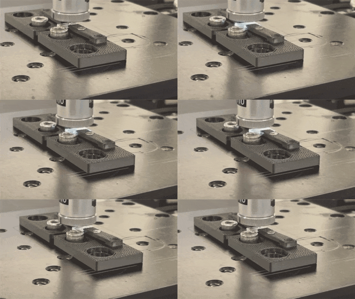
Researchers at the U.S. National Renewable Energy Lab (NREL) in Golden, Colo., say they’ve found a better way to seal solar modules. Using a femtosecond laser, the researchers welded together solar panel glass without the use of polymers such as ethylene vinyl acetate. These glass-to-glass precision welds are strong enough for outdoor solar panels, and are better at keeping out corrosive moisture, the researchers say.

A short video shows a femtosecond laser welding a circular object in a larger rectangle on a workbench. A femtosecond laser welds a small piece of test glass.NREL

“Solar panels are not easily recycled,” says David Young, a senior scientist at NREL. “There are companies that are doing it now, but it’s a tricky play between cost and benefit, and most of the problem is with the polymers.” With no adhesive polymers involved, recycling facilities can more easily separate and reuse the valuable materials in solar panels such as silicon, silver, copper, and glass.

Because of the polymer problem, many recycling facilities just trash the polymer-covered silicon cells and recover only the aluminum frames and glass encasements, says Silvana Ovaitt, a photovoltaic (PV) analyst at NREL. This partial recycling wastes the most valuable materials in the modules.

“At some point there’s going to be a huge amount of spent panels out there, and we want to get it right, and make it easy to recycle.” —David Young, NREL

Finding cost-effective ways to recycle all the materials in solar panels will become increasingly important. Manufacturers globally are deploying enough solar panels to produce an additional 240 gigawatts each year. That rate is projected to increase to 3 terawatts by 2030, Ovaitt says. By 2050, anywhere from 54 to 160 million tonnes of PV panels will have reached the end of their life-spans, she says.

“At some point there’s going to be a huge amount of spent panels out there, and we want to get it right, and make it easy to recycle,” says Young. “There’s no reason not to.” A change in manufacturing could help alleviate the problem—although not for at least another 25 years, when panels constructed with the new technique would be due to be retired.

In NREL’s technique, the glass that encases the solar cells in a PV panel is welded together by precision melting. The precision melting is accomplished with femtosecond lasers, which pack a tremendous number of photons into a very short time scale--about 1 millionth of 1 billionth of a second. The number of photons emitted per second from the laser is so intense that it changes the optical absorption process in the glass, says Young. The process changes from linear (normal absorption) to nonlinear, which allows the glass to absorb energy from the photons that it would normally not absorb, he says.

The intense beam, focused near the interface of the two sheets of glass, generates a small plasma of ionized glass atoms. This plasma allows the glass to absorb most of the photons from the laser and locally melt the two glass sheets to form a weld. Because there’s no open surface, there is no evaporation of the molten glass during the welding process. The lack of evaporation from the molten pool allows the glass to cool in a stress-free state, leaving a very strong weld.

A blue colored micrograph shows 5 horizontal lines and a scale bar of 481 \u00b5m. A femtosecond laser creates precision welds between two glass plates.David Young/NREL

In stress tests conducted by the NREL group, the welds proved almost as strong as the glass itself, as if there were no weld at all. Young and his colleagues described their proof-of-concept technique in a paper published 21 February in the IEEE Journal of Photovoltaics.

This is the first time a femtosecond laser has been used to test glass-to-glass welds for solar modules, the authors say. The cost of such lasers has declined over the last few years, so researchers are finding uses for them in a wide range of applications. For example, femtosecond lasers have been used to create 3D midair plasma displays and to turn tellurite glass into a semiconductor crystal. They’ve also been used to weld glass in medical devices.

Prior to femtosecond lasers, research groups attempted to weld solar panel glass with nanosecond lasers. But those lasers, with pulses a million times as long as those of a femtosecond laser, couldn’t create a glass-to-glass weld. Researchers tried using a filler material called glass frit in the weld, but the bonds of the dissimilar materials proved too brittle and weak for outdoor solar panel designs, Young says.

In addition to making recycling easier, NREL’s design may make solar panels last longer. Polymers are poor barriers to moisture compared with glass, and the material degrades over time. This lets moisture into the solar cells, and eventually leads to corrosion. “Current solar modules aren’t watertight,” says Young. That will be a problem for perovskite cells, a leading next-generation solar technology that is extremely sensitive to moisture and oxygen.

“If we can provide a different kind of seal where we can eliminate the polymers, not only do we get a better module that lasts longer, but also one that is much easier to recycle,” says Young.

❌