Microchip has released the LAN887x family of single-pair gigabit Ethernet transceivers adding to their line of Single Pair Ethernet (SPE) devices. This new family of transceivers supports 100BASE-T1(compliant with IEEE 802bw-2015) and 1000BASE-T1(compliant with IEEE 802.3bp) network speeds and can handle extended cable lengths up to 40 meters. They also integrate time-sensitive networking (TSN) protocols and comply with ISO 26262 functional safety standards. Additionally, they can operate in low
Microchip has released the LAN887x family of single-pair gigabit Ethernet transceivers adding to their line of Single Pair Ethernet (SPE) devices. This new family of transceivers supports 100BASE-T1(compliant with IEEE 802bw-2015) and 1000BASE-T1(compliant with IEEE 802.3bp) network speeds and can handle extended cable lengths up to 40 meters. They also integrate time-sensitive networking (TSN) protocols and comply with ISO 26262 functional safety standards. Additionally, they can operate in low-power mode with features like EtherGREEN technology and OPEN Alliance TC10 sleep mode. All these features make this IC useful for applications such as automotive, industrial, avionics, robotics, and automation fields.
Microchip previously released the LAN8770 100BASE-T1 Ethernet PHY Transceiver which has a max cable length of 15 meters for UTP (Unshielded Twisted Pair) cable and 40 meters for STP (Shielded Twisted Pair) cable. The speed was limited to 100 Mbps, but now, with the release of the new 1000BASE-T1 ethernet controllers, the data transmission speed has been significantly increased to 1 Gbps.
Device – LAN887x family of Ethernet PHY Transceiver
LAN8870 with RGMII and SGMII interfaces, extended cable reach for 1000BASE-T1 Type B (up to 40 meters)
LAN8871 with RGMII interface and similar features as LAN8870, but does not support the extended cable reach for Type B (See Cable reach section for details).
LAN8872 with SGMII interface and similar features as LAN8870, but does not support the extended cable reach for Type B.
Supported standards
IEEE 802.3bw-2015 (100BASE-T1)
IEEE 802.3bp-2016 (1000BASE-T1)
OPEN Alliance TC10 (ultra-low power sleep and wake-up)
IEEE 802.1AS-2020 (Time-Sensitive Networking)
IEEE 1588-2019 (Precision Time Protocol)
MAC interfaces – RGMII and SGMII
Cable reach
Type A – At least 15 meters
Type B (LAN8870B only) – At least 40 meters (potential for even longer reach)
Power management
FlexPWR technology for variable I/O and core power supply
EtherGREEN energy-efficient technology
Diagnostics
Cable defect detection
Receiver Signal Quality Indicator (SQI)
Over-temperature and under-voltage protection
status interrupt support
Loopback and test modes
Misc
Microchip Functional Safety Ready
MicroCHECK design review service available
Time-Sensitive Networking (TSN) ready
Temperature range
Automotive Grade 2: -40°C to +105°C
Industrial: -40°C to +85°C
Package – 48-pin VQFN (7 x 7 mm) with wettable flanks
The main differences between the three ICs are the MAC interface support and 1000BASE-T1 Type B capability. The LAN8870 supports both SGMII and RGMII, whereas the LAN8871 supports only RGMII, and the LAN8872 supports only SGMII. Only LAN8870 supports 1000BASE-T1 Type B with cable reach up to 40 meters. But the LAN8871 and LAN8872 do not support this feature. you can check out the datasheet for the LAN887x family for more information.
Extending single-pair Ethernet cables to 40 meters automatically introduces signal loss and timing issues to the network. The transmitted signal tends to weaken over longer distances which causes errors, especially in noisy environments. Additionally, maintaining proper impedance to avoid signal reflections becomes more difficult, which requires careful design and potentially increasing costs. So I would take the “with cable reaches beyond the IEEE 802.3bp standard of up to at least 15 meters for type A and up to at least 40 meters for type B.” with a grain of salt.
The company mentions that the chips are designed for low power consumption so they have introduced EtherGREEN technology and EN Alliance TC10 ultra-low-power sleep mode together the standby power of this chip goes as low as 16 µA. Additionally, this chip has support for RGMII and SGMII interfaces for design flexibility and simple integration with a wide range of MCUs and SoCs.
At the time of writing the company does not provide any pricing information for the new single-pair gigabit Ethernet transceivers, but you can find a little more information on the Microchips product page or the press release.
YouTuber “EDISON SCIENCE CORNER” has designed yet another Arduino UNO clone but with a twist as the board is made out of a flexible PCB.
Companies like JLCPCB, PCBWay, and others have been offering flexible PCB manufacturing services for a while, mostly for flat cables or small boards that need to fit around a case, but the Flexduino is a complete Arduino UNO clone made of a flex PCB, and it looks rather cool.
The flexible Arduino board does work as shown with the RGB LED and power LED in the
YouTuber “EDISON SCIENCE CORNER” has designed yet another Arduino UNO clone but with a twist as the board is made out of a flexible PCB.
Companies like JLCPCB, PCBWay, and others have been offering flexible PCB manufacturing services for a while, mostly for flat cables or small boards that need to fit around a case, but the Flexduino is a complete Arduino UNO clone made of a flex PCB, and it looks rather cool.
The flexible Arduino board does work as shown with the RGB LED and power LED in the photo above and YouTube video below, but its usefulness is rather limited, and some corners had to be cut as for instance there’s no ground plane.
Nevertheless, it’s a nice demo of flexible PCB technology. The video on the EDISON SCIENCE CORNER channel provides a short demo, shows how the PCB was designed (EasyEDA), and go through the ordering and assembly process. The project files for the Flexduino haven’t been shared as far as I can tell.
Renesas Electronics has introduced the RRH62000, a compact multi-sensor module for indoor air quality monitoring. It integrates particle detection, VOC, and gas sensing with an onboard Renesas MCU for sensor management. The module is designed for use in air purifiers, smoke detectors, HVAC systems, weather stations, and smart home devices.
The RRH62000 is an integrated sensor module that measures key air quality parameters, including particulate matter (PM1, PM2.5, PM10), total volatile organic
Renesas Electronics has introduced the RRH62000, a compact multi-sensor module for indoor air quality monitoring. It integrates particle detection, VOC, and gas sensing with an onboard Renesas MCU for sensor management. The module is designed for use in air purifiers, smoke detectors, HVAC systems, weather stations, and smart home devices.
The RRH62000 is an integrated sensor module that measures key air quality parameters, including particulate matter (PM1, PM2.5, PM10), total volatile organic compounds (TVOC), Indoor Air Quality Index (IAQ), estimated carbon dioxide (eCO2), temperature (T), and relative humidity (RH). These measurements are combined into a single package, with digital outputs available for each sensor, enabling simultaneous measurement. The module features a six-pin connector for easy plug-and-play integration.
The RRH62000 is available with the RRH62000-EVK evaluation kit, which simplifies the testing of the integrated sensor module. The module measures critical air quality parameters and connects to a Windows PC via USB. The evaluation kit includes a USB cable, ESCom board, RRH62000 sensor module, and a Quick Start Guide.
Renesas RRH62000 module specifications
MCU – Onboard Renesas microcontroller
Integrated multi-sensor module for air quality monitoring
Particulate matter (PM1, PM2.5, PM10)
Detects particle sizes from 0.3 µm to 10µm
Mass concentration measurement range: 0 to 1,000 µg/m³
Mass concentration resolution: 1 µg/m³
Number concentration range: 0 to 3,000 particles/cm³
Gas Sensor (ZMOD4410)
TVOC measurement range – 160 to 10,000 ppb
IAQ measurement range – 1 to 5 IAQ
Estimated CO2 (eCO2) range – 400 to 5,000 ppm
Humidity and Temperature Sensor (HS4003)
Humidity range: 0 to 100% RH
Humidity accuracy: ±5 to ±7% RH (20% to 80% RH range)
Temperature range: -40°C to 125°C
Temperature accuracy: ±0.4°C to ±0.55°C (-10°C to 80°C range)
Host interfaces – I2C and UART
Connector – ACES 51468-0064N-001 connector for data output and power
Power Supply
Input voltage: 4.5V to 5.5V
Current consumption during measurement – Max. 60mA
USB Type-C connector for connecting the communication board to the user’s computer
PMOD Connector (Female) for additional sensors via I2C interface
PMOD Connector (Male) for Renesas MCU EVKs
14-pin connector for connecting the environmental sensor boards to the ESCom communication board
Compatible Sensors
ZMOD4410 & RRH46410 for TVOC, IAQ
ZMOD4510 for O3, NO2, OAQ
ZMOD4450 for RAQ
HS3001 & HS4001 for RHT
FS3000 for Air velocity
RRH62000 for PM, TVOC, RHT
Misc
Power LED – Blue when power is ON
Status LED – Blue when ESCom is connected, blinks green when communication takes place
Power Supply
5V via USB-C connector for internal power
1.8V to 3.3V supply with external power supply pin
Dimensions – TBD
Jumper Settings and Connectors on the Environmental Sensor Communication Board
The RRH62000-EVK software, ES-Eval, provides a user-friendly graphical interface for configuring and evaluating the RRH62000 environmental sensor module. It features blocks for measurement control, sensor selection, algorithm configuration, signal analysis, and real-time data visualization, allowing users to easily manage and monitor the sensor’s performance. The software also automatically checks for and installs firmware updates for the ESCom communication board upon startup, ensuring optimal functionality. Users can download ES-Eval from the Software Downloads section on the Renesas website.
ES Eval software interface
The documentation for the kits includes a quick start manual, a list of components (BoM), circuit diagrams, and PCB design files for development and production purposes. all can be found on their respectiveproduct pages.
At the time of writing, I can see that all the major distributors have this board available on their websites including Mouser where the RRH62000 module is available for $38.08 and RRH62000-EVK is sold for $100.
MYIR has recently introduced MYC-LMA35 industrial SoM and its associated development board built around the Nuvoton NuMicro MA35D1 microprocessor with two Arm Cortex-A35 cores and one Arm Cortex-M4 real-time core for processing. The SoM comes in a BGA package with connectivity options such as dual Gigabit Ethernet, cellular connectivity, Wi-Fi/Bluetooth, and various other interfaces like RS232, RS485, USB, CAN, ADC, GPIO, and more. All these features make this SoM and its associated dev board us
MYIR has recently introduced MYC-LMA35 industrial SoM and its associated development board built around the Nuvoton NuMicro MA35D1 microprocessor with two Arm Cortex-A35 cores and one Arm Cortex-M4 real-time core for processing. The SoM comes in a BGA package with connectivity options such as dual Gigabit Ethernet, cellular connectivity, Wi-Fi/Bluetooth, and various other interfaces like RS232, RS485, USB, CAN, ADC, GPIO, and more. All these features make this SoM and its associated dev board useful for demanding edge IIoT applications like industrial automation, energy management systems, smart city infrastructure, and remote monitoring solutions.
M.2 socket and 2x SIM card slots for 4G/5G LTE module (USB-based)
USB
2x USB 2.0 host ports
1x USB 2.0 OTG port
Serial Interface
6x RS232 (isolated)
6x RS485 (isolated)
4x CAN Interfaces (w/ isolation)
Expansion
30-pin GPIO expansion header
2x Digital Input ports, 2x Digital Output ports
1x ADC Interface
Debug – 3x Debug Interfaces (one for Cortex-A35 core, one for Cortex-M4 core, one for SWD)
Misc – Reset, User, Power buttons
Dimensions – 150 x 110mm
Power
12V/2A DC (baseboard)
5V/1A DC (SoM)
Temperature Range – -40°C to 85°C
MYD-LMA35 Development Board Top and BottomMYC-LMA35 System-on-Module (Top view and Bottom view)
In terms of software, the company provides SDK featuring Linux 5.10, which includes u-boot, the kernel, and drivers in source code format which makes it easy to develop applications for the dev board. Moreover, the company also mentions there will be support for Debian and OpenWrt in the future. The documentation also includes pinout descriptions, certifications, and 3D STEP files of the MYC-LMA35 industrial SoM.
The Nuvoton NuMicro MA35D1 industrial SoM is available with either 256MB NAND flash for $39.80 or 8GB eMMC for $45.80. The MYD-LMA35 dev board goes for $99.00 with 256 MB NAND flash and $105 with 8GB eMMC flash. You can find more details and purchasing information on the product page.
After I reviewed the NapCat smart video doorbell last June, the company asked me to review a wireless NVR with solar-powered security cameras and I understood I would receive a kit with four solar-powered cameras and an NVR with storage preinstalled.
In this review, I’ll go through an unboxing, a quick teardown of the NVR, the installation process, and my experience with the Napcat NVR user interfaces (connected to HDMI) and the Napcat Life Android app which I also used with the video doorbell.
Napcat wireless NVR N1S22 kit unboxing
The package I’ve received reads “N1S22” model of a “Solar-powered Security Camera System” and is quite smaller than I expected.
One reason for the small size is that my kit only comes with two cameras instead of four, and the company also did a good job of making everything take as little space as possible. On the net, you’ll see it advertised as a “4K security camera system”, but the included 2.4 GHz WiFi cameras only have a resolution of just 2680×1620 (5MP).
The kit features a compact wireless NVR (center in the photo below), a 12V/2A power adapter for the NVR, an Ethernet cable, an HDMI cable, a USB mouse, two battery-powered security cameras, two small solar panels each with a 3-meter USB-C expansion cord and a solar mounting bracket, as well as a pack of screws, a reset needle pin, some stickers, and a quick start guide.
The NVR system features an HDMI port, an Ethernet RJ45 jack, a USB port for the mouse, a Reset pinhole, a USB port for storage, a microSD card slot (fitted with a 64GB microSD card), and a 12V DC jack.
The bottom side says the Napcat N1 is an 8-channel WiFi network video recorder.
The bottom cover is attached to the main unit through a magnet. You can press on the left or right side to take it out. From there you’ll find the QR code to add the NVR to the Napcat Life app, as well as a SATA tray secured by a screw and suitable for 2.5-inch SATA drives. I’ll just be using the provided microSD card for this review.
The front of the camera has some infrared LEDs, a spotlight (yellow), two indicator lights (red and green), a photosensitive sensor, a hole for a microphone, a PIR motion sensor, and a hole for the speakers on the bottom.
The bottom side of the “B220” camera has waterproof covers for a microSD card slot and a USB-C port for power. Since the videos will be recorded to the NVR, I did not add a microSD card to the cameras. I precharge the cameras with a USB power adapter before installation and connection to the solar panels.
Napcat N1 teardown
The NVR is easy to teardown, so I went ahead and we can see it’s based on a MediaTek MT7628DAN MIPS processor on a module attached to two interesting metal antennas… The main processor is under a heatsink, but it did come off easily, so I left that alone.
The bottom side features the SATA connector for a 2.5-inch hard drive.
Napcat wireless NVR setup
Before installing the cameras, we should make sure everything works first. So I connected the NVR to my router through Ethernet, added the mouse and an HDMI monitor, and connected the power supply.
We are asked to set up a password as the first configuration step. But this needs to be done with the mouse and a software keyboard that pops up. Not ideal. I tried to connect a USB keyboard to the storage port, but it did not work. I was too lazy to type a password with the software keyboard using the mouse, so I went to the Napcat Life mobile app for configuration. I first scanned the QR code under the device after tapping on “+ Add Device” in the app, and went through the configuration wizard.
After the NVR is properly detected, we’re asked to enter a device name, select the time zone, and we’re good to go… Just make sure to disable any VPN including Adblockers you may have when adding the device or it will fail (based on my experience with the video doorbell).
Now that the configuration is done, I went back to the display connected to the NVR and was just asked to input the password I had set in the mobile app.
Somehow, I had to confirm the time zone and date/time formats again…
… before selecting the storage device.
Finally, I was presented with the QR code, but I didn’t need it at this point, so I clicked on “Finish”.
Our two cameras can be seen in a 3×3 Mozaic for eight cameras, so everything is working, and it’s time to install the cameras in strategic locations.
There are various ways to install the cameras. I installed the first camera on the wall directly, and since I don’t have a ladder that would allow me to safely place the solar panel on the roof, I attached it to the cover of an old water pump in an area that gets sun a few hours a day. I did not use the solar panel bracket at all.
Camera 1 (CH1)
I install the second camera the same way but used the solar panel bracket to install the second solar panel in a location that gets sun a couple of hours a day.
Camera 2 (CH2)
At first, I felt the camera holder for the camera was insecure and a bird or strong winds could potentially bring it down, but then I noticed there was also a thread to insert a screw and keep it properly secured.
One other method is placing the camera directly into the solar panel bracket, but this would not have worked in my case due to the locations of the cameras not getting any sun at all. It’s also possible to mount it on the holding bracket provided with the kit, but that is probably not suitable for outdoor use since the holding bracket is simply placed on the surface and there aren’t any screws to secure it.
Napcat wireless NVR user interface
Once the installation is complete, we can go back to the NVR and check out the interface. Our two cameras are properly shown, but the live window shows paused videos because the cameras are only active when a person, vehicle, or motion is detected in order to save power and extend the battery life.
We can manually start each stream by clicking the blue play button with the mouse. We are asked to enter the NVR password each time we want to start using the device after a period of inactivity. I tried to disable it in the configuration menu but was unable to find a suitable option.
Nighttime capture also works well in black and white. The camera also has a color night vision option, but the spotlight is rather weak, so colors are not as good as a product like the Foscam SPC.
Color night vision screenshot from Napcat Life app
Besides the “Live” window, we can access other menus by clicking the Home icon on the top left corner of the display.
The Playback menu enables the other to check videos by day, watch them, and edit them as needed.
The Search menu is similar, but more useful, as it will show the more recent videos each with a thumbnail showing the person that was detected.
Clicking a video will enlarge the video and we can perform the same operations as in the Playback window…
… including zooming in on suspect individuals…
The Configuration section has various options for channel settings, display settings, encoding, privacy protection to define those where recording should be hidden, and camera maintenance.
The Events and Alarm option should that only pedestrian detection is enabled by default. Vehicle detection and motion detection are both turned off, but that’s fine in the current location of the cameras since car can’t access those locations or disabling motion detection extends the battery life.
I haven’t shown all configuration menus here, but everything is pretty standard. The NVR can be connected to WiFi instead of Ethernet if indeed, as in all battery-powered WiFi cameras I’ve tested so far ONVIF and RTSP are not supported since they are better suited to cameras operating 24/7.
I still did a quick test to see what would happen if I turned off my broadband router, meaning the NVR would exclusively operate in the LAN without access to the Internet. Everything worked like before. I could play the live videos, and human detection is working fine. Since it rained at the time, I also used an umbrella in a way that prevented the camera from seeing my face and upper body, but a pedestrian was still detected properly.
Napcat Life app
I connected the broadband router and went to the Napcat Life app. The settings are pretty common except for a few items.
I first went to the message notification section because I would not receive any notifications on my phone, but everything seems fine, and I’m unable to make that work. I can only manually check notifications when I get inside the app.
The Deterrence section also intrigued me… It’s used to enable the siren and strobe lights, but it did not work until I went to the Smart Event->Pedestrian & Vehicle Detection, and manually set Deterrence to ON there. The siren is quite loud, you can listen to it in the video below.
The rest of the app is pretty much standard and similar to the NVR interface with a Live and a Playback section…
You can select from some of the latest videos, or filter the videos for a given day.
Sadly, Download does not seem to work properly as it’s telling me the file will be downloaded to “Person Center->Albums”, but I’m unable to find any videos after download. It’s the exact same issue as in the Napcat smart video doorbell review two months ago… It’s disappointing.
Conclusion
The Napcat wireless NVR works reasonably well and is easy to install with solar-powered security cameras so no cabling is required through the house. Like most/all? recent security cameras, it supports AI features such as pedestrian and vehicle detection greatly reducing the number of false positives.
The camera outputs can be visualized through the NVR connected to an HDMI display and mouse, or through the Napcat Life mobile app for Android or iOS. The system works offline without access to the internet when visualizing the cameras from the NVR’s display.
Like other battery-powered WiFi cameras, I’ve tested the Napcat cameras do not support standard streaming protocols such as ONVIF or RTSP which means you are dependent on the company staying in business, at least when using the mobile app. I understand that ONVIF may not be suitable for battery-powered cameras, but I’ve tested cameras from five different vendors, and each requires its own app. I wish some standard like Matter could be more widespread. Another very disappointing issue is the download feature does not work from the mobile app, so it’s unclear how people can save important videos if needed.
I’d like to thank Napcap for sending the N1S22 wireless NVR kit for review. The kit can be purchased on Amazon for $299.99 after ticking on the $70 discount, and kits with four and six cameras go for $479.99 (with $100 discount) and $759.99 (no discount) on the same page.
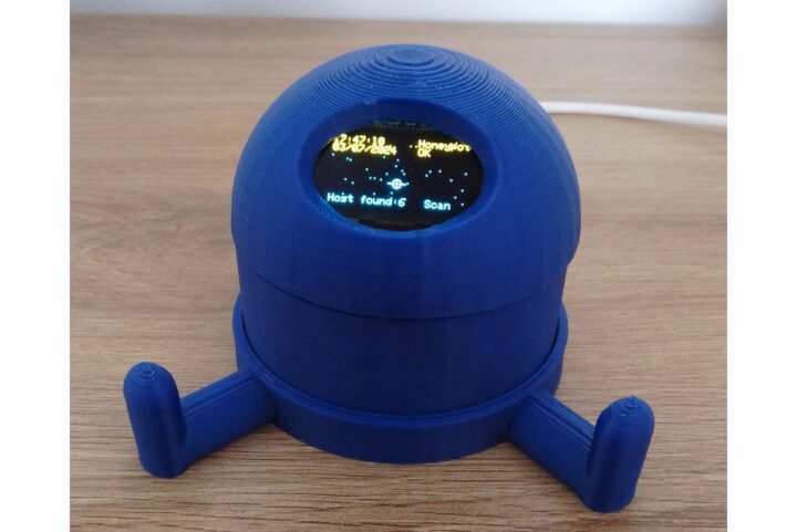
The Netgotchi network security scanner is a simple, compact device based on an ESP8266 wireless microcontroller with a single goal: to defend your home network from intruders and potential bad actors. It is described as “Pwnagotchi’s older brother,” a network guardian that keeps your network safe instead of penetrating it.
If you are unfamiliar with Pwnagotchi, it is an A2C-based (advantage actor-critic) “AI” that can penetrate Wi-Fi networks using WPA key material obtained from passive sniffin
The Netgotchi network security scanner is a simple, compact device based on an ESP8266 wireless microcontroller with a single goal: to defend your home network from intruders and potential bad actors. It is described as “Pwnagotchi’s older brother,” a network guardian that keeps your network safe instead of penetrating it.
If you are unfamiliar with Pwnagotchi, it is an A2C-based (advantage actor-critic) “AI” that can penetrate Wi-Fi networks using WPA key material obtained from passive sniffing or de-authentication attacks. The Netgotchi is a reverse Pwnagotchi that alerts you to intruders or breaches in your network. It runs on a simple microcontroller and cannot employ reinforcement learning like the Pwnagotchi. Rather, it pings the network periodically and reports any new potential security threats.
The device’s design is as simple as its purpose. It is an ESP8266 microcontroller connected to an OLED display and running an Arduino .ino script, enclosed in a 3D-printed case. It is powered via USB and does not contain batteries, so an external power bank is required for portable use.
Netgotchi wiring diagram
The Netgotchi software is open-source and available in ESP32 and ESP8266 versions in the GitHub repository, alongside an installation guide. The device has been tested and is compatible with Minigotchi firmware. Minigotchi is a currently archived project that is essentially a tiny Pwnagotchi, and performs deauth attacks and advertisements.
The Netgotchi scanner is limited to 2.4GHz Wi-Fi networks and will scan compatible networks at intervals. It scans hosts for vulnerable services such as Telnet, FTP, SSH, and HTTP and marks them as “WRNG!” to indicate a potential security risk. The “WRNG!” indicator can be toggled on or off using the securityScanActive flag. The Honeypot functionality exposes a service to lure potential intruders and triggers an alarm when breached. The scanner features a web interface and supports a headless mode for cyberdecks and other devices.
The Netgotchi network security scanner is priced at $69 on Tindie and comes pre-assembled with a USB cable in the box. Multiple color options are available on request. Due to the device’s open-source nature, there is no post-sale warranty.
There aren’t a lot of open-source devices aimed primarily at identifying security threats on your home network, but you may be interested in deauthentication hardware such as the Flipper Zero add-on, the Marauder Pocket Unit, and the Deauther Watch X.
ALLPCB is an ideal PCB manufacturer for PCB professionals and businesses thanks to additional customization options compared to competitors, monthly discounts for business users, and post-delivery payment options, besides ultra-fast delivery services and quality assurance services.
ALLPCB customization options
ALLPCB excels at higher specification boards and more complex PCB designs, which is why ALLPCB provides more customized quote options than competitors. Let’s take JLCPCB, one of ALLPCB’s m
ALLPCB is an ideal PCB manufacturer for PCB professionals and businesses thanks to additional customization options compared to competitors, monthly discounts for business users, and post-delivery payment options, besides ultra-fast delivery services and quality assurance services.
ALLPCB customization options
ALLPCB excels at higher specification boards and more complex PCB designs, which is why ALLPCB provides more customized quote options than competitors. Let’s take JLCPCB, one of ALLPCB’s main competitors, as an example starting with “Surface Finish” options for FR-4 material.
JLCPCB PCB specifications
JLCPCB offers three options, namely HASL (with lead), LeadFree HASL, and ENIG, but ALLPCB offers a total of 12 different surface finish options.
That would the the same first three as in JLCPCB, but also
ALLPCB also offers a PTH (Plating Through Hole) copper thickness option from
You can discover more customization options such as selecting our prepreg for various applications on ALLPCB’s online quote system.
A business-friendly PCB manufacturer
ALLPCB has a business verification program designed to enhance efficiency and reduce costs for business users. It offers business users monthly discounts and post-delivery payment options. After the verification, a business can have net 30-day payment terms to help with their cash flow. Also, they can enjoy ALLPCB prototyping services each month for a minimum cost of 1$.
ALLPCB’s PCB batch order prices are highly competitive. Aluminum PCBs start at $50 per square meter, and 6-layer PCBs start at $110 per square meter.
The company also recognizes the importance of time to market. ALLPCB offers significantly faster delivery times compared to industry standards. For example, 6-layer board batch orders (under 5 square meters) can be produced in just 3 days, while aluminum PCB batch orders (under 10 square meters) are produced in 2 days. This is 3-5 days faster than what competitors typically provide.
Quality assurance is equally important and all solder masks are even and thick, PCBs have smooth edges, and silkscreens are clear and accurate.
Give ALLPCB a try for just $1 with 1-6 layer PCB
If you think your business might benefit from ALLPCB PCB manufacturing services, you can have the opportunity to test the service for just $1 for an order of 5 pieces with up to 6 layers and a size of up to 150x100mm. You can check out the ordering process in our previous article about the promotion.
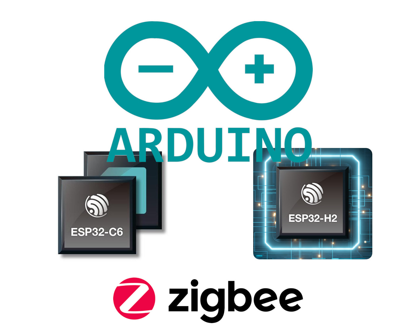
Some of the newer Espressif Systems wireless SoCs such as the ESP32-H2 and ESP32-C6 support Zigbee through their built-in 802.15.4 radio. It’s been working since the release of the ESP-IDF 5.1 framework along with the ESP-Zigbee-SDK for a while, but Arduino support was less straightforward.
But this is about to change as an Espressif engineer nicknamed P-R-O-C-H-Y has recently added a Zigbee wrapper library for the ESP-Zigbee-SDK to Arduino Core for ESP32 that works with ESP32-C6 and ESP32-H2 as
But this is about to change as an Espressif engineer nicknamed P-R-O-C-H-Y has recently added a Zigbee wrapper library for the ESP-Zigbee-SDK to Arduino Core for ESP32 that works with ESP32-C6 and ESP32-H2 as standalone nodes and other SoC can be used as radio co-processor attached to an RPC (802.15.4 radio layer).
The wrapper library currently supports the following:
Zigbee classes and all Zigbee roles
Zigbee network scanning
Allow multiple endpoints on the same Zigbee device (not tested yet)
Supported Home Assistant devices
On/off light + switch
Color Dimmable light + switch
Setting Manufacturer and model name
Other tasks currently planned include supporting “Temperature sensor + Thermostat” Home Assistant devices, updating ported examples to use the Zigbee library, and writing documentation… While the latter is still missing, you’ll find four basic Arduino code samples for the following Zigbee devices: a light bulb, a light switch, a temperature sensor, and a thermostat.
You can follow the progress of the port on GitHub or even contribute if you are interested in adding to the features. Over time this could potentially benefit open-source Arduino projects such as Tasmota which could add support for ESP32-C6 and ESP32-H2’s Zigbee connectivity on top of existing support for Zigbee MCUs from Texas Instruments (CC253X, CC26x2, CC13x2) and Silicon Labs (EFR32MG12/EFRMG21).
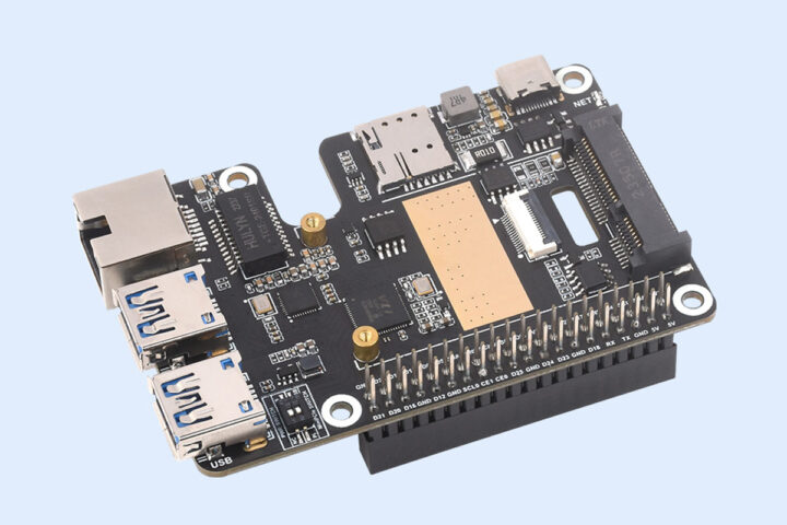
Waveshare has recently introduced the PCIe to MiniPCIe GbE USB3.2 HAT+ for Raspberry Pi 5 adding gigabit Ethernet, a mini PCIe socket for 4G LTE, and two USB 3.2 Gen1 ports to the popular Arm single board computer. The HAT+ is compatible with IM7600G-H-PCIE/EG25-G-mPCIe series 4G LTE modules with 4G/3G/2G global band and GNSS positioning. Additionally, it has a gigabit Ethernet with an onboard RJ45 port, two USB 3.2 Gen1 ports, an onboard power monitoring chip, and EEPROM. All these features mak
Waveshare has recently introduced the PCIe to MiniPCIe GbE USB3.2 HAT+ for Raspberry Pi 5 adding gigabit Ethernet, a mini PCIe socket for 4G LTE, and two USB 3.2 Gen1 ports to the popular Arm single board computer. The HAT+ is compatible with IM7600G-H-PCIE/EG25-G-mPCIe series 4G LTE modules with 4G/3G/2G global band and GNSS positioning. Additionally, it has a gigabit Ethernet with an onboard RJ45 port, two USB 3.2 Gen1 ports, an onboard power monitoring chip, and EEPROM. All these features make this HAT useful for applications such as industrial routers, home gateways, set-top boxes, industrial laptops, industrial PDAs, and much more.
2x USB 3.2 Gen1 ports driven by VL805 PCIe to USB 3.2 Gen1 HUB IC
USB Type-C interface for 4G networking, firmware updates, or external power supply
GPIO – Raspberry Pi GPIO header
Misc
Onboard power monitoring chip (INA219)
EEPROM
DIP switches for power control and USB signal direction
LED indicators for power and network status
Power Supply – 3V ~ 3.6V (5V through USB)
Dimensions – 65 x 56 mm
Operating Temperature – -40°C to +80°C
While it’s great to have a multi-interface HAT+ board, the PCIe interface of the Raspberry Pi 5 only supports up to PCIe Gen3 x1 with a maximum bandwidth of 8 Gbps. This HAT adds Gigabit Ethernet (1 Gbps), two USB 3.2 Gen 1 (2x 5 Gbps theoretical), and a 4G LTE module (variable bandwidth depending on network conditions) to the Raspberry Pi 5. So, there’s a good chance that the Pi’s PCIe bandwidth could become a bottleneck if you’re trying to max out the speeds of multiple interfaces simultaneously.
So, If you’re planning on using this HAT for demanding applications, then you should consider the Raspberry Pi 5’s PCIe bandwidth and plan accordingly.
PCIe TO MiniPCIe GbE USB3.2 HAT+ board details and pinout
As the device is plug-and-play the company mentions that the board supports Raspberry Pi OS, Ubuntu, OpenWrt, and other operating systems with reliable network speeds. Waveshare also provides installation instructions and demos on how to use the power monitoring IC with the Raspberry Pi 5.
PCIe to MiniPCIe GbE USB3.2 HAT+ Installation Instruction
The board has an operating temperature range of -40°C to +80°C and can be used for industrial applications such as rugged IPCs and digital signage, as well as routers, laptops, and tablets used in industrial settings. But bear in mind that Raspberry Pi Limited did not specify an operating temperature range for the Pi 5.
The PCIe TO MiniPCIe GbE USB3.2 HAT+ is available on Aliexpress for $29.46 and on Amazon for $37.43. If you need the 4G and GPS functionality, you can bundle the HAT with the SIM7600G-H 4G module and antennas, bringing the cost to $70.06 on Aliexpress and $95.99 on Amazon. You can also check out the Waveshare store for additional purchase options, but Waveshare’s pricing does not include shipping.
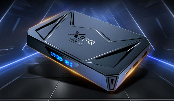
X96Q Pro+ is an Android 14 TV box powered by the new Allwinner H728 octa-core Cortex-A55 SoC with a Mali-G57-MC1 GPU, and a 4Kp60 / 8Kp24 H.265 and VP9 4Kp60 video decoder that looks very similar to the Allwinner T527 AIoT SoC.
The TV box ships with 4GB RAM and 32GB eMMC flash by default, and features an HDMI 2.0 port outputting up to 4K at 60 Hz, a 3.5mm audio jack, an optical S/PDIF output, a gigabit Ethernet port, WiFi 6 and Bluetooth 5.0 connectivity, and a few USB ports.
X96Q Pro+ specific
X96Q Pro+ is an Android 14 TV box powered by the new Allwinner H728 octa-core Cortex-A55 SoC with a Mali-G57-MC1 GPU, and a 4Kp60 / 8Kp24 H.265 and VP9 4Kp60 video decoder that looks very similar to the Allwinner T527 AIoT SoC.
The TV box ships with 4GB RAM and 32GB eMMC flash by default, and features an HDMI 2.0 port outputting up to 4K at 60 Hz, a 3.5mm audio jack, an optical S/PDIF output, a gigabit Ethernet port, WiFi 6 and Bluetooth 5.0 connectivity, and a few USB ports.
X96Q Pro+ specifications:
SoC – Allwinner H728
CPU – Octa-core Arm Cortex-A55 processor in two clusters of four cores four cores
Package – FCCSP 660 balls
17 mm x 17 mm size, 0.5 mm ball pitch, 0.3 mm ball size
Manufacturing process – 22nm ULP
System Memory – 4GB (2GB optional)
Storage
32GB eMMC flash (16/64GB optional)
MicroSD card slot
Video Output – HDMI 2.0a up to 4Kp60 with 10-bit HDR support
Audio – 3.5mm audio jack, optical S/PDIF, digital audio via HDMI
Networking
Gigabit Ethernet port
Dual-band WiFi 6 and Bluetooth 5.0
USB – 1x USB 3.0 port, 2x USB 2.0 ports
Misc
Power button
Update pinhole
Front panel display
Optional RTC
Power Supply – 5V/3A via DC jack
Dimensions – 140 x 90 x 20mm
Weight – 150 grams
The TV box ships with a remote control, a power adapter, an HDMI cable, and a user manual. The main benefit of the X96Q Pro+ is that it runs the most recent Android 14 (for TV?) operating system. The Allwinner H728 “Decoding Platform Processor” does have some interesting interfaces like PCIe 2.1 x1, 30x PWM, two gigabit Ethernet MAC, and more that make it look like the Allwinner T527 even more, so it’s probably just handled by a different business unit within Allwinner, and that’s potentially the same silicon.
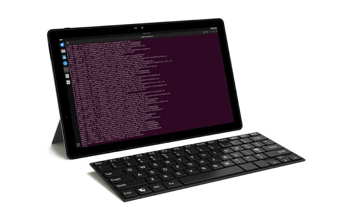
DeepComputing DC-ROMA RISC-V Pad II is a 10.1-inch tablet based on the same SpacemIT K1 octa-core 64-bit RISC-V processor found in the DC-ROMA RISC-V Laptop II introduced a few months ago, as well as in the MILK-V Jupiter mini-ITX motherboard.
The RISC-V tablet features up to 16GB LPDDR4, 128GB eMMC flash, a 10.1-inch capacitive touchscreen display with 1920×1200 resolution, a 5MP rear camera, a 2MP webcam, a USB-C port for peripherals and/or an external display, and a 6,000 mAh battery.
DC-ROM
DeepComputing DC-ROMA RISC-V Pad II is a 10.1-inch tablet based on the same SpacemIT K1 octa-core 64-bit RISC-V processor found in the DC-ROMA RISC-V Laptop II introduced a few months ago, as well as in the MILK-V Jupiter mini-ITX motherboard.
The RISC-V tablet features up to 16GB LPDDR4, 128GB eMMC flash, a 10.1-inch capacitive touchscreen display with 1920×1200 resolution, a 5MP rear camera, a 2MP webcam, a USB-C port for peripherals and/or an external display, and a 6,000 mAh battery.
Networking – Not specified, but potentially Wi-Fi 6 & Bluetooth 5.2 like in the laptop
USB – 1x USB 3.2 Gen 1 Type-C port with DisplayPort Alt mode
Battery – 3.5V/6,000 mAh (max) cobalt battery
Power Supply – Via USB-C port (TBC)
Dimensions and Weight – TBD
The tablet runs Ubuntu 24.04 right now, but DeepComputing says models with 16GB RAM will be upgradeable to Android 15 AOSP in Q4 2024… Please note that while Linux RISC-V support has made great progress, our review of the Jupiter RISC-V motherboard based on the same SpacemIT M1/K1 revealed more work is needed. I still think the Android 15 release schedule is probably way too optimistic since Android 15 AOSP is yet to be released…
If you are a developer interested in checking out the RISC-V tablet, you can pre-order it with a 20% deposit for as low as $149 in the 4GB/64GB configuration. The top model with 16GB RAM and a 128GB eMMC flash goes for $299. A few more details may be found in the press release, and the tablet is currently showcased at the RISC-V Summit China 2024 in Hangzhou until August 25.
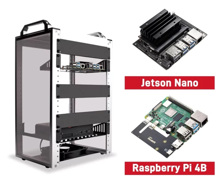
DeskPi RackMate T1 is a U8 desktop rack especially suited to SBC users with support for Raspberry Pi SBCs, NVIDIA Jetson developer kits, Raxa ROCK 5B pico-ITX SBC, mini-ITX motherboards, and more.
The RackMate T1 chassis is made of aluminum alloy and acrylic frame and its 8U form factor (406 (H) x 280 (L) x 200 (W) mm) allows it to be placed either on a desk or a floor of a home lab.
DeskPi RackMat T1 highlights:
Mounting holes on all trays
Raspberry Pi 3B, 3B, +4B, and DeskPi aux board bring
DeskPi RackMate T1 is a U8 desktop rack especially suited to SBC users with support for Raspberry Pi SBCs, NVIDIA Jetson developer kits, Raxa ROCK 5B pico-ITX SBC, mini-ITX motherboards, and more.
The RackMate T1 chassis is made of aluminum alloy and acrylic frame and its 8U form factor (406 (H) x 280 (L) x 200 (W) mm) allows it to be placed either on a desk or a floor of a home lab.
DeskPi RackMat T1 highlights:
Mounting holes on all trays
Raspberry Pi 3B, 3B, +4B, and DeskPi aux board bring HDMI and USB-C to the front (M2.5 screws) – star holes
Radxa ROCK 5B pico-ITX SBC (M3 screws) – round holes
2.5-inch drives
Screw kits with M2.5 screws and standoffs, M3 screws, and a screwdriver
Dimensions – 406 x 280 x 200 mm (H x L x W)
Materials – Aluminum alloy and acrylic frame
The documentation is extremely poor with low-resolution images and confusion with “optional accessories” that are shown in all photos as if they were included:
Rack shell
Blank panel
SBC shell
Mini-ITX shell
10-inch network switch
For example, I can see at least three blank panels, one rack shell, and one SBC shell in the kit below. One would assume those are included, but it’s hard to tell since the company does not make it specific.
It’s not the first time we have written about rack solutions for Raspberry Pi and other SBCs, and we previously covered a 19-inch rackmount from MyElectronics taking up to 16 Raspberry Pi boards, which may be more cost-effective for European users although you’d need to bring your own rack/chassis.
The DeskPi RackMate T1, also called the “GeeekPi 8U Server Cabinet” can be purchased for $179.99 on Amazon and most users seem happy about it, except one that received a kit with a cracked top acrylic panel. The accessories mentioned above sell for $12 to $36 on Amazon. TheRackMate T1 can also be purchased on the company’s store, but they don’t recommend it due to hefty shipping charges from China…
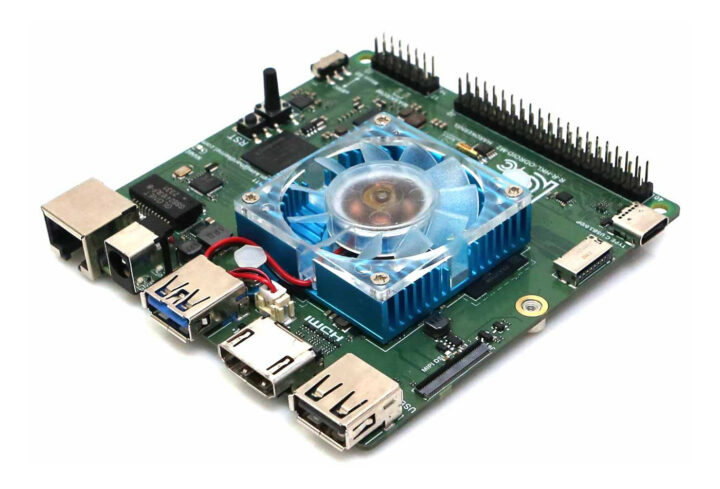
Hardkernel has just launched the ODROID-M2 low-profile SBC based on a Rockchip RK3588S2 octa-core Cortex-A76/A55 AI SoC with up to 16GB LPDDR5, 64GB eMMC flash, an M.2 PCIe socket, support for three displays through HDMI, USB-C, and MIPI DSI interfaces, gigabit Ethernet, and more.
The ODROID-M2 follows the ODROID-M1 and ODROID-M1S single board computers based on respectively Rockchip RK3568 and RK3566 quad-core Cortex-A55 processors, but a significantly more powerful Rockchip RK3588S2 processor,
Hardkernel has just launched the ODROID-M2 low-profile SBC based on a Rockchip RK3588S2 octa-core Cortex-A76/A55 AI SoC with up to 16GB LPDDR5, 64GB eMMC flash, an M.2 PCIe socket, support for three displays through HDMI, USB-C, and MIPI DSI interfaces, gigabit Ethernet, and more.
CPU – Octa-core processor with 4x Cortex-A76 cores @ up to 2.3 GHz (+/- 0.1Ghz), 4x Cortex-A55 cores @ up to 1.8 GHz
GPU – Arm Mali-G610 MP4 GPU @ 1 GHz compatible with OpenGL ES 3.2, OpenCL 2.2, and Vulkan 1.2 APIs
VPU – 8Kp60 video decoder for H.265/AVS2/VP9/H.264/AV1 codecs, 8Kp30 H.265/H.264 video encoder
AI accelerator – 6 TOPS (INT8) NPU
System Memory – 8GB or 16GB 64-bit LPDDR5 (4GB RAM variant coming soon).
Storage
64GB eMMC flash
MicroSD card slot with UHS-I SDR104 mode support
M.2 M-Key socket with PCIe 2.1 x1 for NVMe SSDs
Video output
HDMI 2.0 up to 4K @ 60Hz with HDR, EDID
DisplayPort via USB-C port
30-pin MIPI DSI connector (note: different from the 31-pin connector on the ODROID-M1)
Networking – Gigabit Ethernet RJ45 port
USB
USB 2.0 host port
USB 3.0 host port
USB 3.0 Type-C port with DP Alt-Mode (not a power source/sink)
Expansion
40-pin Raspberry Pi-compatible GPIO header
14-pin GPIO header
Debugging – Serial debug console
Misc
Power button, Reset button
System LEDs
Red (POWER) – Solid light when DC power is connected
Blue (ALIVE) – Flashing like a heartbeat while the Linux kernel is running, solid light in u-boot.
PCF8536 RTC with CR2032 backup battery holder
Boot priority switch for eMMC or microSD card
Power Supply – 7.5V to 15.5V DC input via 5.5/2.1mm power barrel jack; 12V/2A power adapter recommended
Power Consumption (Hardkernel numbers)
Power Off – About 0 Watt
IDLE – About 1Watt without any peripherals
CPU stress test – About 7.5 Watts (Performance governor) without any peripherals
Dimensions – 90 x 90 x 21mm
Weight – 78g including heatsink, 58g without heatsink
ODROID-M2 fitted with M.2 SSD
ODROID-M2 block diagram
You may have heard about the RK3588S, but not necessarily about the RK3588S2, and we wondered about the difference between the two in our Radxa ROCK 5C article:
how does RK3588S2 differ from RK3588S? They are basically the same except the RK3588S2 comes with an additional MIPI CSI interface which is not used in the ROCK 5C.
The MIPI CSI interface is not used in the ODROID-M2 either, but there must be a good reason why both companies selected the RK3588S2 instead, either pricing or availability…
In terms of performance, Hardkernel explains the ODROID-M2 is better than the ODROID-M1S in every way:
Multicore performance is about 3 times faster.
About twice the memory bandwidth with LPDDR5 64-bit RAM
The Mali-610 GPU is over 5 times faster.
The 6TOPS NPU is over 3 times faster.
The 64GB eMMC flash is twice as fast thanks to an HS400 interface.
ODROID-M1 vs ODROID-N2+ vs ODROID-M2 benchmark comparison
One downside is that the new ODROID-M2 is fitted with a heatsink with a fan for cooling, while the earlier models could operate fanlessly. Having said that, Hardkernel mentions the fan seldom rotates in the video below, so I’d assume some people may just decide to disconnect the fan.
Hardkernel is usually better than most other SBC vendors when it comes to software support. We typically just get a list of operating systems, but the Korean company goes into more detail when it comes to software features.
Android 13
Based on AOSP
Customized raw GPIO access framework (in other words, GPIOs works in Android).
SPI ( CAN receiver, LED strip lights, IO expander)
Ubuntu 24.04 with a newer kernel version will be released in a few months
You can see a short demo in Android 13 with two 4K displays one playing a 4K video and the other running 3DMark with 3D graphics acceleration. More details about the hardware and software can be found on the wiki.
Hardkernel sells the ODROID-M2 SBC on its own store for $115 with 8GB LPDDR5, 64GB eMMC flash, and an enclosure, while the 16GB RAM model goes for $145. The upcoming 4GB RAM model will sell for under $100, more exactly for $95 once it becomes available.
Mekotronics R58-4×4 3S is another Rockchip RK3588-based Arm PC and digital signage player from the company with unusual features such as a 3-inch display on the front panel as well as four HDMI inputs supporting up to 4Kp60 sources.
The embedded PC features up to 16GB RAM and 128GB eMMC flash, an M.2 PCIe socket for NVMe storage, an 8Kp60-capable HDMI 2.1 video output port, gigabit Ethernet and WiFi 6 connectivity, a mini PCIe socket and NanoSIM card slot for a 4G LTE/GPS module, and more.
Meko
Mekotronics R58-4×4 3S is another Rockchip RK3588-based Arm PC and digital signage player from the company with unusual features such as a 3-inch display on the front panel as well as four HDMI inputs supporting up to 4Kp60 sources.
The embedded PC features up to 16GB RAM and 128GB eMMC flash, an M.2 PCIe socket for NVMe storage, an 8Kp60-capable HDMI 2.1 video output port, gigabit Ethernet and WiFi 6 connectivity, a mini PCIe socket and NanoSIM card slot for a 4G LTE/GPS module, and more.
M.2 M-Key (PCIe 3.0) socket for an M.2 2280 NVMe SSD
MicroSD card slot
Video Output
HDMI 2.1 port up to 8Kp60
Internal LVDS connector
Video Input – 4x HDMI inputs up to 4Kp60
Display – 3-inch display connected over MIPI DSI
Audio – 3.5mm jacks “audio”, Line-in, and Line-out
Networking
Gigabit Ethernet RJ45 jack
WiFi 6
Optional 4G LTE/GPS module via mini PCIe socket and nano SIM card slot
Up to two external antennas
USB – 2x USB 3.0, 2x USB 2.0, 1x USB Type-C port
Expansion
Internal GPIO header
M.2 socket for storage
Mini PCIe socket + NanoSIM card slot for cellular connectivity
Misc
Power button
Front panel buttons (D-Pad, 3x user buttons)
RTC clock
Power Supply – 12V/3A via 5.5×2.1mm DC jack
Dimensions – TBD (Aluminum enclosure)
Two HDMI inputs can be found on the left side and two HDMI inputs on the right side.
The company provides support for Android 12, Debian, and Armbian (Ubuntu) operating systems as well as Buildroot built system. We don’t have that many extra details at this time, but the company showcases the Arm PC with Android 12 in the video below showing the 3-inch display mirroring the HDMI output, and also demonstrating the HDMI input feature.
We were not given pricing information for this specific model. More details may be found on the product page.
MeatPi Electronics introduced the WiCAN Pro, an ESP32-S3-based OBD scanner, and the successor to WiCAN-OBD. Equipped with an OBD-II interface IC, it provides full support for all legislated OBD-II protocols. It offers compatibility with multiple CAN Bus protocols, including three standard CAN Bus and single-wire CAN Bus.
The previous generation WiCAN module came in an OBD or USB-based version. The WiCAN Pro only has an OBD interface, but another significant difference from the previous product i
MeatPi Electronics introduced the WiCAN Pro, an ESP32-S3-based OBD scanner, and the successor to WiCAN-OBD. Equipped with an OBD-II interface IC, it provides full support for all legislated OBD-II protocols. It offers compatibility with multiple CAN Bus protocols, including three standard CAN Bus and single-wire CAN Bus.
The previous generation WiCAN module came in an OBD or USB-based version. The WiCAN Pro only has an OBD interface, but another significant difference from the previous product is that it features a USB host port. This port can power USB devices up to 1.5 amps at 5 volts and enables capabilities like adding GPS or cellular-based radios, like with meatPi’s ESPNetLink add-on.
The WiCAN Pro plugs into the vehicle’s OBD port and is powered by the vehicle’s battery. The voltage range is 6.5V to 18V, consuming about 35mA during operation and 2.8mA in sleep mode.
ESP32-S3-based OBD scanner WiCAN Pro PCB
The device includes dual UARTs, one dedicated to flashing and debugging the ESP32-S3 and the other configurable for sending commands to the OBD chip, providing flexibility for developers working on custom automotive applications. According to the product page, WiCAN Pro can be integrated with Home Assistant and other IoT applications without requiring external apps. This feature enables users to incorporate vehicle data into a smart home ecosystem, allowing for automated vehicle diagnostics and monitoring.
Graphical Diagram of WiCan Pro
The ESP32-S3-based OBD scanner WiCAN Pro runs on the versatile WiCAN firmware, which is already available and runs on an ESP32. This firmware can send MQTT messages about the vehicle’s health, integrate with Home Assistant, or drive a RealDash display with real-time information. Moreover, this open-source device is compatible with a range of established OBD diagnostic apps including Car Scanner, Torque Lite or Pro, OBD Auto Doctor, BimmerCode, and OBD Fusion.
RealDash dashboard example. More designs can be found in the RealDash gallery
The company also offers a feature comparison between the WiCAN Pro, WiCAN, and the OBDLink MX+.
The WiCAN Pro campaign launched on Crowd Supply and has raised $6,000 so far with 35 days remaining. The product is priced at $80, with an additional $8 for U.S. shipping and $18 for international shipping. Deliveries are expected to start by mid-February 2025.
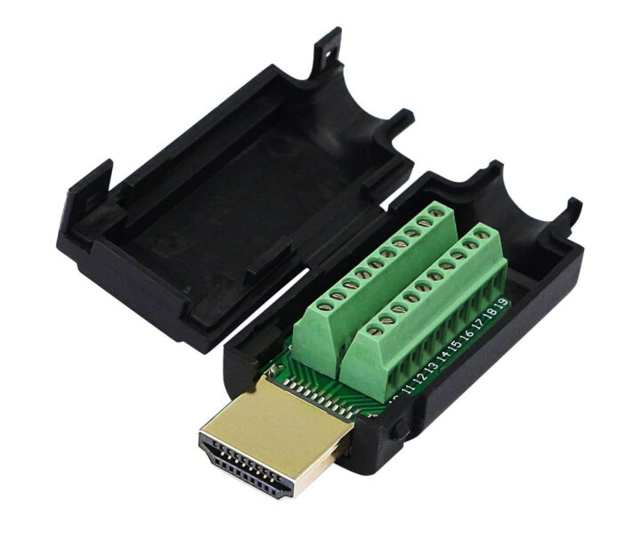
The very idea of an HDMI to screw terminal adapters maybe seem moronic at first, but in an era of programmable IOs (PIO), and high-speed serial transmit (HSTX), those could end up being useful for boards or modules based on Raspberry Pi RP2040 or RP2350 since they’ve all be shown to support DVI output through HDMI connectors.
There are a few boards that integrate an HDMI port such as the Olimex RP2040-PICO-PC, Solder Party RP2xxx Stamp Carrier XL, or Adafruit Feather RP2040 among others, but mos
There are a few boards that integrate an HDMI port such as the Olimex RP2040-PICO-PC, Solder Party RP2xxx Stamp Carrier XL, or Adafruit Feather RP2040 among others, but most boards don’t include an HDMI port. What they do typically have are GPIO headers, and an HDMI to screw terminal adapter would allow users to easily add an HDMI port to their existing board without soldering simply by using jumper wires, or with a bit more work an old HDMI cable.
All HDMI to screw terminal adapters are pretty basic with an HDMI male connector compatible with HDMI 2.0 (24AWG) and two terminal blocks with 10 poles each all housed in a plastic enclosure. No soldering is required unless your module/board does not come with headers with only through or castellated holes.
While there are 20 pins in total wiring to a Raspberry Pi RP2040 should only require about 11 pins based on the schematics for the PicoDVI project.
NVIDIA on Tuesday said that future monitor scalers from MediaTek will support its G-Sync technologies. NVIDIA is partnering with MediaTek to integrate its full range of G-Sync technologies into future monitors without requiring a standalone G-Sync module, which makes advanced gaming features more accessible across a broader range of displays.
Traditionally, G-Sync technology relied on a dedicated G-sync module – based on an Altera FPGA – to handle syncing display refresh rates with the GPU in o
NVIDIA on Tuesday said that future monitor scalers from MediaTek will support its G-Sync technologies. NVIDIA is partnering with MediaTek to integrate its full range of G-Sync technologies into future monitors without requiring a standalone G-Sync module, which makes advanced gaming features more accessible across a broader range of displays.
Traditionally, G-Sync technology relied on a dedicated G-sync module – based on an Altera FPGA – to handle syncing display refresh rates with the GPU in order to reduce screen tearing, stutter, and input lag. As a more basic solution, in 2019 NVIDIA introduced G-Sync Compatible certification and branding, which leveraged the industry-standard VESA AdaptiveSync technology to handle variable refresh rates. In lieu of using a dedicated module, leveraging AdaptiveSync allowed for cheaper monitors, with NVIDIA's program serving as a stamp of approval that the monitor worked with NVIDIA GPUs and met NVIDIA's performance requirements. Still, G-Sync Compatible monitors still lack some features that, to date, require the dedicated G-Sync module.
Through this new partnership with MediaTek, MediaTek will bring support for all of NVIDIA's G-Sync technologies, including the latest G-Sync Pulsar, directly into their scalers. G-Sync Pulsar enhances motion clarity and reduces ghosting, providing a smoother gaming experience. In addition to variable refresh rates and Pulsar, MediaTek-based G-Sync displays will support such features as variable overdrive, 12-bit color, Ultra Low Motion Blur, low latency HDR, and Reflex Analyzer. This integration will allow more monitors to support a full range of G-Sync features without having to incorporate an expensive FPGA.
The first monitors to feature full G-Sync support without needing an NVIDIA module include the AOC Agon Pro AG276QSG2, Acer Predator XB273U F5, and ASUS ROG Swift 360Hz PG27AQNR. These monitors offer 360Hz refresh rates, 1440p resolution, and HDR support.
What remains to be seen is which specific MediaTek's scalers will support NVIDIA's G-Sync technology – or if the company is going to implement support into all of their scalers going forward. It also remains to be seen whether monitors with NVIDIA's dedicated G-Sync modules retain any advantages over displays with MediaTek's scalers.
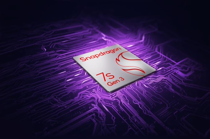
Qualcomm this morning is taking the wraps off of a new smartphone SoC for the mid-range market, the Snapdragon 7s Gen 3. The second of Qualcomm’s down-market ‘S’ tier Snapdragon 7 parts, the 7s series is functionally the entry-level tier for the Snapdragon 7 family – and really, most Qualcomm-powered handsets in North America.
With three tiers of Snapdragon 7 chips, the 7s can easily be lost in the noise that comes with more powerful chips. But the latest iteration of the 7s is a bit more inter
Qualcomm this morning is taking the wraps off of a new smartphone SoC for the mid-range market, the Snapdragon 7s Gen 3. The second of Qualcomm’s down-market ‘S’ tier Snapdragon 7 parts, the 7s series is functionally the entry-level tier for the Snapdragon 7 family – and really, most Qualcomm-powered handsets in North America.
With three tiers of Snapdragon 7 chips, the 7s can easily be lost in the noise that comes with more powerful chips. But the latest iteration of the 7s is a bit more interesting than usual, as rather than reusing an existing die, Qualcomm has seemingly minted a whole new die for this part. As a result, the company has upgraded the 7s family to use Arm’s current Armv9 CPU cores, while using bits and pieces of Qualcomm’s latest IPs elsewhere.
Qualcomm Snapdragon 7-Class SoCs
SoC
Snapdragon 7 Gen 3
(SM7550-AB)
Snapdragon 7s Gen 3
(SM7635)
Snapdragon 7s Gen 2
(SM7435-AB)
CPU
1x Cortex-A715
@ 2.63GHz
3x Cortex-A715
@ 2.4GHz
4x Cortex-A510
@ 1.8GHz
1x Cortex-A720
@ 2.5GHz
3x Cortex-A720
@ 2.4GHz
4x Cortex-A520
@ 1.8GHz
4x Cortex-A78
@ 2.4GHz
4x Cortex-A55
@ 1.95GHz
GPU
Adreno
Adreno
Adreno
DSP / NPU
Hexagon
Hexagon
Hexagon
Memory
Controller
2x 16-bit CH
@ 3200MHz LPDDR5 / 25.6GB/s
@ 2133MHz LPDDR4X / 17.0GB/s
2x 16-bit CH
@ 3200MHz LPDDR5 / 25.6GB/s
@ 2133MHz LPDDR4X / 17.0GB/s
2x 16-bit CH
@ 3200MHz LPDDR5 / 25.6GB/s
@ 2133MHz LPDDR4X / 17.0GB/s
ISP/Camera
Triple 12-bit Spectra ISP
1x 200MP or 64MP with ZSL or
32+21MP with ZSL or
3x 21MP with ZSL
4K HDR video & 64MP burst capture
Triple 12-bit Spectra ISP
1x 200MP or 64MP with ZSL or
32+21MP with ZSL or
3x 21MP with ZSL
4K HDR video & 64MP burst capture
Triple 12-bit Spectra ISP
1x 200MP or 48MP with ZSL or
32+16MP with ZSL or
3x 16MP with ZSL
4K HDR video & 48MP burst capture
Encode/
Decode
4K60 10-bit H.265
H.265, VP9 Decoding
Dolby Vision, HDR10+, HDR10, HLG
1080p120 SlowMo
4K60 10-bit H.265
H.265, VP9 Decoding
HDR10+, HDR10, HLG
1080p120 SlowMo
4K60 10-bit H.265
H.265, VP9 Decoding
HDR10, HLG
1080p120 SlowMo
Integrated Radio
FastConnect 6700
Wi-Fi 6E + BT 5.3
2x2 MIMO
FastConnect
Wi-Fi 6E + BT 5.4
2x2 MIMO
FastConnect 6700
Wi-Fi 6E + BT 5.2
2x2 MIMO
Integrated Modem
X63 Integrated
(5G NR Sub-6 + mmWave)
DL = 5.0 Gbps 5G/4G Dual Active SIM (DSDA)
Integrated
(5G NR Sub-6 + mmWave)
DL = 2.9 Gbps 5G/4G Dual Active SIM (DSDA)
X62 Integrated
(5G NR Sub-6 + mmWave)
DL = 2.9 Gbps 5G/4G Dual Active SIM (DSDA)
Mfc. Process
TSMC N4P
TSMC N4P
Samsung 4LPE
Officially, the Snapdragon 7s is classified as a 1+3+4 design – meaning there’s 1 prime core, 3 performance cores, and 4 efficiency cores. In this case, Qualcomm is using the same architecture for both the prime and efficiency cores, Arm’s current-generation Cortex-A720 design. The prime core gets to turbo as high as 2.5GHz, while the remaining A720 cores will turbo as high as 2.4GHz.
These are joined by the 4 efficiency cores, which, as is tradition, are based upon Arm’s current A5xx cores, in this case, A520. These can boost as high as 1.8GHz.
Compared to the outgoing Snapdragon 7s Gen 2, the switch in Arm cores represents a fairly significant upgrade, replacing an A78/A55 setup with the aforementioned A720/A520 setup. Notably, clockspeeds are pretty similar to the previous generation part, so most of the unconstrained performance uplift on this generation is being driven by improvements in IPC, though the faster prime core should offer a bit more kick for single-threaded workloads.
All told, touting a 20% improvement in CPU performance over the 7s Gen 2, though that claim doesn’t clarify whether it’s single or multi-threaded performance (or a mixture of both).
Meanwhile, graphics are driven by one of Qualcomm’s Adreno GPUs. As is usually the case, the company is not offering any significant details on the specific GPU configuration being used – or even what generation it is. A high-level look at the specifications doesn’t reveal any major features that weren’t present in other Snapdragon 7 parts. And Qualcomm isn’t bringing high-end features like ray tracing down to such a modest part. That said, I’ve previously heard through the tea leaves that this may be a next-generation (Adreno 800 series) design; though if that’s the case, Qualcomm is certainly not trying to bring attention to it.
Curiously, however, the video decode block on the SoC seems rather dated. Despite this being a new die, Qualcomm has opted not to include AV1 decoding – or, at least, opted not to enable it – so H.265 and VP9 are the most advanced codecs supported.
Compared to CPU performance gains, Qualcomm’s expected GPU performance gains are more significant. The company is claiming that the7s Gem 3 will deliver a 40% improvement in GPU performance over the 7s Gen 2.
Finally, the Hexagon NPU block on the SoC incorporates some of Qualcomm’s latest IP, as the company continues their focused AI push across all of their chip segments. Notably, the version of the NPU used here gets INT4 support for low precision client inference, which is new to the Snapdragon 7s family. As with Qualcomm’s other Gen 3 SoCs, the big drive here is for local (on-device) LLM execution.
With regards to performance, Qualcomm says that customers should expect to see a 30% improvement in AI performance relative to the 7s Gen 2.
Feeding all of these blocks is a 32-bit memory controller. Interestingly, Qualcomm has opted to support older LPDDR4X even with this newer chip, so the maximum memory bandwidth depends on the memory type used. For LPDDR4X-4266 that will be 17GB/sec, and for LPDDR5-6400 that will be 25.6GB/sec. In both cases, this is identical to the bandwidth available for the 7s Gen 2.
Rounding out the package, the 7s Gen 3 does incorporate some newer/more powerful camera hardware as well. We’re still looking at a trio of 12-bit Spectra ISPs, but the maximum resolution in zero shutter lag and burst modes has been bumped up to 64MPix. Video recording capabilities are otherwise identical on paper, as the 7s Gen 2 already supported 4K HDR capture.
Meanwhile on the wireless communication side of matters, the 7s Gen 3 packs one of Qualcomm’s integrated Snapdragon 5G modems. As with its predecessor, the 7s Gen 3 supports both Sub-6 and mmWave bands, with a maximum (theoretical) throughput of 2.9Gbps.
Eagle-eyed chip watchers will note, however, that Qualcomm is doing away with any kind of version information as of this part. So while the 7s Gen 2 used a Snapdragon X62 modem, the 7s Gen 3’s modem has no such designation – it’s merely an integrated Snapdragon modem. According to the company, this change has been made to “simplify overall branding and to be consistent with other IP blocks in the chipset.”
Similarly, the Wi-Fi/Bluetooth block has lost its version number; it is now merely a FastConnect block. In regards to features and specifications, this appears to be the same Wi-Fi 6E block that we’ve seen in half a dozen other Snapdragon SoCs, offering 2 spatial streams at channel widths up to 160MHz. It is worth noting, however, that since this is a newer SoC it’s certified for Bluetooth 5.4 support, versus the 5.2/5.3 certification other Snapdragon 7 chips have carried.
Finally, the Snapdragon 7s Gen 3 itself is being built on TSMC’s N4P process, the same process we’ve seen the last several Qualcomm SoCs use. And with this, Qualcomm has now fully migrated the entire Snapdragon 8 and Snapdragon 7 lines off of Samsung’s 4nm process nodes; all of their contemporary chips are now built at TSMC. And like similar transitions in the past, this shift in process nodes is coming with a boost to power efficiency. While it’s not the sole cause, overall Qualcomm is touting a 12% improvement in power savings.
Wrapping things up, Qualcomm’s launch customer for the Snapdragon 7s Gen 3 will be Xiaomi, who will be the first to launch a new phone with the chip. Following them will be many of the other usual suspects, including Realme and Sharp, while the much larger Samsung is also slated to use the chip at some point in the coming months.
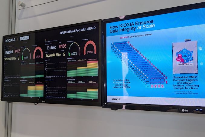
The CXL consortium has had a regular presence at FMS (which rechristened itself from 'Flash Memory Summit' to the 'Future of Memory and Storage' this year). Back at FMS 2022, the company had announced v3.0 of the CXL specifications. This was followed by CXL 3.1's introduction at Supercomputing 2023. Having started off as a host to device interconnect standard, it had slowly subsumed other competing standards such as OpenCAPI and Gen-Z. As a result, the specifications started to encompass a wide
The CXL consortium has had a regular presence at FMS (which rechristened itself from 'Flash Memory Summit' to the 'Future of Memory and Storage' this year). Back at FMS 2022, the company had announced v3.0 of the CXL specifications. This was followed by CXL 3.1's introduction at Supercomputing 2023. Having started off as a host to device interconnect standard, it had slowly subsumed other competing standards such as OpenCAPI and Gen-Z. As a result, the specifications started to encompass a wide variety of use-cases by building a protocol on top of the the ubiquitous PCIe expansion bus. The CXL consortium comprises of heavyweights such as AMD and Intel, as well as a large number of startup companies attempting to play in different segments on the device side. At FMS 2024, CXL had a prime position in the booth demos of many vendors.
The migration of server platforms from DDR4 to DDR5, along with the rise of workloads demanding large RAM capacity (but not particularly sensitive to either memory bandwidth or latency), has opened up memory expansion modules as one of the first set of widely available CXL devices. Over the last couple of years, we have had product announcements from Samsung and Micron in this area.
SK hynix CMM-DDR5 CXL Memory Module and HMSDK
At FMS 2024, SK hynix was showing off their DDR5-based CMM-DDR5 CXL memory module with a 128 GB capacity. The company was also detailing their associated Heterogeneous Memory Software Development Kit (HMSDK) - a set of libraries and tools at both the kernel and user levels aimed at increasing the ease of use of CXL memory. This is achieved in part by considering the memory pyramid / hierarchy and relocating the data between the server's main memory (DRAM) and the CXL device based on usage frequency.
The CMM-DDR5 CXL memory module comes in the SDFF form-factor (E3.S 2T) with a PCIe 3.0 x8 host interface. The internal memory is based on 1α technology DRAM, and the device promises DDR5-class bandwidth and latency within a single NUMA hop. As these memory modules are meant to be used in datacenters and enterprises, the firmware includes features for RAS (reliability, availability, and serviceability) along with secure boot and other management features.
SK hynix was also demonstrating Niagara 2.0 - a hardware solution (currently based on FPGAs) to enable memory pooling and sharing - i.e, connecting multiple CXL memories to allow different hosts (CPUs and GPUs) to optimally share their capacity. The previous version only allowed capacity sharing, but the latest version enables sharing of data also. SK hynix had presented these solutions at the CXL DevCon 2024 earlier this year, but some progress seems to have been made in finalizing the specifications of the CMM-DDR5 at FMS 2024.
Microchip and Micron Demonstrate CZ120 CXL Memory Expansion Module
Micron had unveiled the CZ120 CXL Memory Expansion Module last year based on the Microchip SMC 2000 series CXL memory controller. At FMS 2024, Micron and Microchip had a demonstration of the module on a Granite Rapids server.
Additional insights into the SMC 2000 controller were also provided.
The CXL memory controller also incorporates DRAM die failure handling, and Microchip also provides diagnostics and debug tools to analyze failed modules. The memory controller also supports ECC, which forms part of the enterprise class RAS feature set of the SMC 2000 series. Its flexibility ensures that SMC 2000-based CXL memory modules using DDR4 can complement the main DDR5 DRAM in servers that support only the latter.
Marvell Announces Structera CXL Product Line
A few days prior to the start of FMS 2024, Marvell had announced a new CXL product line under the Structera tag. At FMS 2024, we had a chance to discuss this new line with Marvell and gather some additional insights.
Unlike other CXL device solutions focusing on memory pooling and expansion, the Structera product line also incorporates a compute accelerator part in addition to a memory-expansion controller. All of these are built on TSMC's 5nm technology.
The compute accelerator part, the Structera A 2504 (A for Accelerator) is a PCIe 5.0 x16 CXL 2.0 device with 16 integrated Arm Neoverse V2 (Demeter) cores at 3.2 GHz. It incorporates four DDR5-6400 channels with support for up to two DIMMs per channel along with in-line compression and decompression. The integration of powerful server-class ARM CPU cores means that the CXL memory expansion part scales the memory bandwidth available per core, while also scaling the compute capabilities.
Applications such as Deep-Learning Recommendation Models (DLRM) can benefit from the compute capability available in the CXL device. The scaling in the bandwidth availability is also accompanied by reduced energy consumption for the workload. The approach also contributed towards disaggregation within the server for a better thermal design as a whole.
The Structera X 2404 (X for eXpander) will be available either as a PCIe 5.0 (single x16 or two x8) device with four DDR4-3200 channels (up to 3 DIMMs per channel). Features such as in-line (de)compression, encryption / decryption, and secure boot with hardware support are present in the Structera X 2404 as well. Compared to the 100 W TDP of the Structera X 2404, Marvell expects this part to consume around 30 W. The primary purpose of this part is to enable hyperscalers to recycle DDR4 DIMMs (up to 6 TB per expander) while increasing server memory capacity.
Marvell also has a Structera X 2504 part that supports four DDR5-6400 channels (with two DIMMs per channel for up to 4 TB per expander). Other aspects remain the same as that of the DDR4-recycling part.
The company stressed upon some unique aspects of the Structera product line - the inline compression optimizes available DRAM capacity, and the 3 DIMMs per channel support for the DDR4 expander maximizes the amount of DRAM per expander (compared to competing solutions). The 5nm process lowers the power consumption, and the parts support accesses from multiple hosts. The integration of Arm Neoverse V2 cores appears to be a first for a CXL accelerator, and enables delegation of compute tasks to improve overall performance of the system.
While Marvell announced specifications for the Structera parts, it does appear that sampling is at least a few quarters away. One of the interesting aspects about Marvell's roadmaps / announcements in recent years has been their focus on creating products tuned to the demands of high-volume customers. The Structera product line is no different - hyperscalers are hungry to recycle their DDR4 memory modules and apparently can't wait to get their hands on the expander parts.
CXL is just starting its slow ramp-up, and the hockey stick segment of the growth curve is definitely definitely not in the near term. However, as more host systems with CXL support start to get deployed, products like the Structera accelerator line start to make sense from a server efficiency viewpoint.
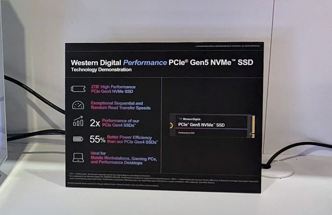
When Western Digital introduced its Ultrastar DC SN861 SSDs earlier this year, the company did not disclose which controller it used for these drives, which made many observers presume that WD was using an in-house controller. But a recent teardown of the drive shows that is not the case; instead, the company is using a controller from Fadu, a South Korean company founded in 2015 that specializes on enterprise-grade turnkey SSD solutions.
The Western Digital Ultrastar DC SN861 SSD is aimed at p
When Western Digital introduced its Ultrastar DC SN861 SSDs earlier this year, the company did not disclose which controller it used for these drives, which made many observers presume that WD was using an in-house controller. But a recent teardown of the drive shows that is not the case; instead, the company is using a controller from Fadu, a South Korean company founded in 2015 that specializes on enterprise-grade turnkey SSD solutions.
The Western Digital Ultrastar DC SN861 SSD is aimed at performance-hungry hyperscale datacenters and enterprise customers which are adopting PCIe Gen5 storage devices these days. And, as uncovered in photos from a recent Storage Review article, the drive is based on Fadu's FC5161 NVMe 2.0-compliant controller. The FC5161 utilizes 16 NAND channels supporting an ONFi 5.0 2400 MT/s interface, and features a combination of enterprise-grade capabilities (OCP Cloud Spec 2.0, SR-IOV, up to 512 name spaces for ZNS support, flexible data placement, NVMe-MI 1.2, advanced security, telemetry, power loss protection) not available on other off-the-shelf controllers – or on any previous Western Digital controllers.
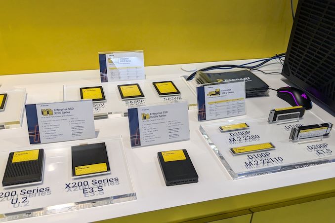
The Ultrastar DC SN861 SSD offers sequential read speeds up to 13.7 GB/s as well as sequential write speeds up to 7.5 GB/s. As for random performance, it boasts with an up to 3.3 million random 4K read IOPS and up to 0.8 million random 4K write IOPS. The drives are available in capacities between 1.6 TB and 7.68 TB with one or three drive writes per day (DWPD) over five years rating as well as in U.2 and E1.S form-factors.
While the two form factors of the SN861 share a similar technical design, Western Digital has tailored each version for distinct workloads: the E1.S supports FDP and performance enhancements specifically for cloud environments. By contrast, the U.2 model is geared towards high-performance enterprise tasks and emerging applications like AI.
Without any doubts, Western Digital's Ultrastar DC SN861 is a feature-rich high-performance enterprise-grade SSD. It has another distinctive feature: a 5W idle power consumption, which is rather low by the standards of enterprise-grade drives (e.g., it is 1W lower compared to the SN840). While the difference with predecessors may be just 1W, hyperscalers deploy thousands of drives and for their TCO every watt counts.
Western Digital's Ultrastar DC SN861 SSDs are now available for purchase to select customers (such as Meta) and to interested parties. Prices are unknown, but they will depend on such factors as volumes.
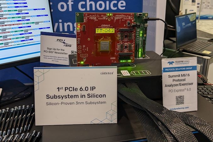
As the deployment of PCIe 5.0 picks up steam in both datacenter and consumer markets, PCI-SIG is not sitting idle, and is already working on getting the ecosystem ready for the updats to the PCIe specifications. At FMS 2024, some vendors were even talking about PCIe 7.0 with its 128 GT/s capabilities despite PCIe 6.0 not even starting to ship yet. We caught up with PCI-SIG to get some updates on its activities and have a discussion on the current state of the PCIe ecosystem.
PCI-SIG has alrea
As the deployment of PCIe 5.0 picks up steam in both datacenter and consumer markets, PCI-SIG is not sitting idle, and is already working on getting the ecosystem ready for the updats to the PCIe specifications. At FMS 2024, some vendors were even talking about PCIe 7.0 with its 128 GT/s capabilities despite PCIe 6.0 not even starting to ship yet. We caught up with PCI-SIG to get some updates on its activities and have a discussion on the current state of the PCIe ecosystem.
PCI-SIG has already made the PCIe 7.0 specifications (v 0.5) available to its members, and expects full specifications to be officially released sometime in 2025. The goal is to deliver a 128 GT/s data rate with up to 512 GBps of bidirectional traffic using x16 links. Similar to PCIe 6.0, this specification will also utilize PAM4 signaling and maintain backwards compatibility. Power efficiency as well as silicon die area are also being kept in mind as part of the drafting process.
The move to PAM4 signaling brings higher bit-error rates compared to the previous NRZ scheme. This made it necessary to adopt a different error correction scheme in PCIe 6.0 - instead of operating on variable length packets, PCIe 6.0's Flow Control Unit (FLIT) encoding operates on fixed size packets to aid in forward error correction. PCIe 7.0 retains these aspects.
The integrators list for the PCIe 6.0 compliance program is also expected to come out in 2025, though initial testing is already in progress. This was evident by the FMS 2024 demo involving Cadence's 3nm test chip for its PCIe 6.0 IP offering along with Teledyne Lecroy's PCIe 6.0 analyzer. These timelines track well with the specification completion dates and compliance program availability for previous PCIe generations.
We also received an update on the optical workgroup - while being optical-technology agnostic, the WG also intends to develop technology-specific form-factors including pluggable optical transceivers, on-board optics, co-packaged optics, and optical I/O. The logical and electrical layers of the PCIe 6.0 specifications are being enhanced to accommodate the new optical PCIe standardization and this process will also be done with PCIe 7.0 to coincide with that standard's release next year.
The PCI-SIG also has ongoing cabling initiatives. On the consumer side, we have seen significant traction for Thunderbolt and external GPU enclosures. However, even datacenters and enterprise systems are moving towards cabling solutions as it becomes evident that disaggregation of components such as storage from the CPU and GPU are better for thermal design. Additionally maintaining signal integrity over longer distances becomes difficult for on-board signal traces. Cabling internal to the computing systems can help here.
OCuLink emerged as a good candidate and was adopted fairly widely as an internal link in server systems. It has even made an appearance in mini-PCs from some Chinese manufacturers in its external avatar for the consumer market, albeit with limited traction. As speeds increase, a widely-adopted standard for external PCIe peripherals (or even connecting components within a system) will become imperative.
The growth in the enterprise SSD (eSSD) market has outpaced that of the client SSD market over the last few years. The requirements of AI servers for both training and inference has been the major impetus in this front. In addition to the usual vendors like Samsung, Solidigm, Micron, Kioxia, and Western Digital serving the cloud service providers (CSPs) and the likes of Facebook, a number of companies have been at work inside China to service the burgeoning eSSD market within.
In our coverage o
The growth in the enterprise SSD (eSSD) market has outpaced that of the client SSD market over the last few years. The requirements of AI servers for both training and inference has been the major impetus in this front. In addition to the usual vendors like Samsung, Solidigm, Micron, Kioxia, and Western Digital serving the cloud service providers (CSPs) and the likes of Facebook, a number of companies have been at work inside China to service the burgeoning eSSD market within.
In our coverage of the Microchip Flashtec 5016, we had noted Longsys's use of Microchip's SSD controllers to prepare and market enterprise SSDs under the FORESEE brand. Long before that, two companies - DapuStor and Memblaze - started releasing eSSDs specifically focusing on the Chinese market.
There are two drivers for the current growth spurt in the eSSD market. On the performance side, usage of eTLC behind a Gen 5 controller is allowing vendors to advertise significant benefits over the Gen 4 drives in the previous generation. At the same time, a capacity play is happening where there is a race to cram as much NAND as possible into a single U.2 / EDSFF enclosure. QLC is being used for this purpose, and we saw a number of such 128 TB-class eSSDs on display at FMS 2024.
DapuStor and Memblaze have both been relying on SSD controllers from Marvell for their flagship drives. Their latest product iterations for the Gen 5 era use the Marvell Bravera SC5 controller. Similar to the Flashtec controllers, these are not meant to be turnkey solutions. Rather, the SSD vendor has considerable flexibility in implementing specific features for their desired target market.
At FMS 2024, both DapuStor and Memblaze were displaying their latest solutions for the Gen 5 market. Memblaze was celebrating the sale of 150K+ units of their flagship Gen 5 solution - the PBlaze7 7940 incorporating Micron's 232L 3D eTLC with Marvell's Bravera SC5 controller. This SSD (available in capacities up to 30.72 TB) boasts of 14 GBps reads / 10 GBps writes along with random read / write performance of 2.8 M / 720K - all with a typical power consumption south of 16 W. Additionally, the support for some of NVMe features such as software-enabled flash (SEF) and zoned name space (ZNS) had helped Memblaze and Marvell to receive a 'Best of Show' award under the 'Most Innovative Customer Implementation' category.
DapuStor had their current lineup on display (including the Haishen H5000 series with the same Bravera SC5 controller). Additionally, the company had an unannounced proof-of-concept 61.44 TB QLC SSD on display. Despite the label carrying the Haishen5 series tag (its current members all use eTLC NAND), this sample comes with QLC flash.
DapuStor has already invested resources into implementing the flexible data placement (FDP) NVMe feature into the firmware of this QLC SSD. The company also had an interesting presentation session dealing with usage of CXL memory expansion to store the FTL for high-capacity enterprise SSDs - though this is something for the future and not related to any current product in the market.
Having established themselves within the Chinese market, both DapuStor and Memblaze are looking to expand in other markets. Having products with leading performance numbers and features in the eSSD growth segment will stand them in good stead in this endeavor.
At FMS 2024, Phison devoted significant booth space to their enterprise / datacenter SSD and PCIe retimer solutions, in addition to their consumer products. As a controller / silicon vendor, Phison had historically been working with drive partners to bring their solutions to the market. On the enterprise side, their tie-up with Seagate for the X1 series (and the subsequent Nytro-branded enterprise SSDs) is quite well-known. Seagate supplied the requirements list and had a say in the final firmwa
At FMS 2024, Phison devoted significant booth space to their enterprise / datacenter SSD and PCIe retimer solutions, in addition to their consumer products. As a controller / silicon vendor, Phison had historically been working with drive partners to bring their solutions to the market. On the enterprise side, their tie-up with Seagate for the X1 series (and the subsequent Nytro-branded enterprise SSDs) is quite well-known. Seagate supplied the requirements list and had a say in the final firmware before qualifying the drives themselves for their datacenter customers. Such qualification involves a significant resource investment that is possible only by large companies (ruling out most of the tier-two consumer SSD vendors).
Phison had demonstrated the Gen 5 X2 platform at last year's FMS as a continuation of the X1. However, with Seagate focusing on its HAMR ramp, and also fighting other battles, Phison decided to go ahead with the qualification process for the X2 process themselves. In the bigger scheme of things, Phison also realized that the white-labeling approach to enterprise SSDs was not going to work out in the long run. As a result, the Pascari brand was born (ostensibly to make Phison's enterprise SSDs more accessible to end consumers).
Under the Pascari brand, Phison has different lineups targeting different use-cases: from high-performance enterprise drives in the X series to boot drives in the B series. The AI series comes in variants supporting up to 100 DWPD (more on that in the aiDAPTIVE+ subsection below).
The D200V Gen 5 took pole position in the displayed drives, thanks to its leading 61.44 TB capacity point (a 122.88 TB drive is also being planned under the same line). The use of QLC in this capacity-focused line brings down the sustained sequential write speeds to 2.1 GBps, but these are meant for read-heavy workloads.
The X200, on the other hand, is a Gen 5 eTLC drive boasting up to 8.7 GBps sequential writes. It comes in read-centric (1 DWPD) and mixed workload variants (3 DWPD) in capacities up to 30.72 TB. The X100 eTLC drive is an evolution of the X1 / Seagate Nytro 5050 platform, albeit with newer NAND and larger capacities.
These drives come with all the usual enterprise features including power-loss protection, and FIPS certifiability. Though Phison didn't advertise this specifically, newer NVMe features like flexible data placement should become part of the firmware features in the future.
100 GBps with Dual HighPoint Rocket 1608 Cards and Phison E26 SSDs
Though not strictly an enterprise demo, Phison did have a station showing 100 GBps+ sequential reads and writes using a normal desktop workstation. The trick was installing two HighPoint Rocket 1608A add-in cards (each with eight M.2 slots) and placing the 16 M.2 drives in a RAID 0 configuration.
HighPoint Technology and Phison have been working together to qualify E26-based drives for this use-case, and we will be seeing more on this in a later review.
aiDAPTIV+ Pro Suite for AI Training
One of the more interesting demonstrations in Phison's booth was the aiDAPTIV+ Pro suite. At last year's FMS, Phison had demonstrated a 40 DWPD SSD for use with Chia (thankfully, that fad has faded). The company has been working on the extreme endurance aspect and moved it up to 60 DWPD (which is standard for the SLC-based cache drives from Micron and Solidigm).
At FMS 2024, the company took this SSD and added a middleware layer on top to ensure that workloads remain more sequential in nature. This drives up the endurance rating to 100 DWPD. Now, this middleware layer is actually part of their AI training suite targeting small business and medium enterprises who do not have the budget for a full-fledged DGX workstation, or for on-premises fine-tuning.
Re-training models by using these AI SSDs as an extension of the GPU VRAM can deliver significant TCO benefits for these companies, as the costly AI training-specific GPUs can be replaced with a set of relatively low-cost off-the-shelf RTX GPUs. This middleware comes with licensing aspects that are essentially tied to the purchase of the AI-series SSDs (that come with Gen 4 x4 interfaces currently in either U.2 or M.2 form-factors). The use of SSDs as a caching layer can enable fine-tuning of models with a very large number of parameters using a minimal number of GPUs (not having to use them primarily for their HBM capacity).
Intel has divested its entire stake in Arm Holdings during the second quarter, raising approximately $147 million. Alongside this, Intel sold its stake in cybersecurity firm ZeroFox and reduced its holdings in Astera Labs, all as part of a broader effort to manage costs and recover cash amid significant financial challenges.
The sale of Intel's 1.18 million shares in Arm Holdings, as reported in a recent SEC filing, comes at a time when the company is struggling with substantial financial losse
Intel has divested its entire stake in Arm Holdings during the second quarter, raising approximately $147 million. Alongside this, Intel sold its stake in cybersecurity firm ZeroFox and reduced its holdings in Astera Labs, all as part of a broader effort to manage costs and recover cash amid significant financial challenges.
The sale of Intel's 1.18 million shares in Arm Holdings, as reported in a recent SEC filing, comes at a time when the company is struggling with substantial financial losses. Despite the $147 million generated from the sale, Intel reported a $120 million net loss on its equity investments for the quarter, which is a part of a larger $1.6 billion loss that Intel faced during this period.
In addition to selling its stake in Arm, Intel also exited its investment in ZeroFox and reduced its involvement with Astera Labs, a company known for developing connectivity platforms for enterprise hardware. These moves are in line with Intel's strategy to reduce costs and stabilize its financial position as it faces ongoing market challenges.
Despite the divestment, Intel's past investment in Arm was likely driven by strategic considerations. Arm Holdings is a significant force in the semiconductor industry, with its designs powering most mobile devices, and, for obvious reasons, Intel would like to address these. Intel and Arm are also collaborating on datacenter platforms tailored for Intel's 18A process technology. Additionally, Arm might view Intel as a potential licensee for its technologies and a valuable partner for other companies that license Arm's designs.
Intel's investment in Astera Labs was also a strategic one as the company probably wanted to secure steady supply of smart retimers, smart cable modems, and CXL memory controller, which are used in volumes in datacenters and Intel is certainly interested in selling as many datacenter CPUs as possible.
Intel's financial struggles were highlighted earlier this month when the company released a disappointing earnings report, which led to a 33% drop in its stock value, erasing billions of dollars of capitalization. To counter these difficulties, Intel announced plans to cut 15,000 jobs and implement other expense reductions. The company has also suspended its dividend, signaling the depth of its efforts to conserve cash and focus on recovery. When it comes to divestment of Arm stock, the need for immediate financial stabilization has presumably taken precedence, leading to the decision.
Earlier this month, AMD launched the first two desktop CPUs using their latest Zen 5 microarchitecture: the Ryzen 7 9700X and the Ryzen 5 9600X. As part of the new Ryzen 9000 family, it gave us their latest Zen 5 cores to the desktop market, as AMD actually launched Zen 5 through their mobile platform last month, the Ryzen AI 300 series (which we reviewed).
Today, AMD is launching the remaining two Ryzen 9000 SKUs first announced at Computex 2024, completing the current Ryzen 9000 product stack
Earlier this month, AMD launched the first two desktop CPUs using their latest Zen 5 microarchitecture: the Ryzen 7 9700X and the Ryzen 5 9600X. As part of the new Ryzen 9000 family, it gave us their latest Zen 5 cores to the desktop market, as AMD actually launched Zen 5 through their mobile platform last month, the Ryzen AI 300 series (which we reviewed).
Today, AMD is launching the remaining two Ryzen 9000 SKUs first announced at Computex 2024, completing the current Ryzen 9000 product stack. Both chips hail from the premium Ryzen 9 series, which includes the flagship Ryzen 9 9950X, which has 16 Zen 5 cores and can boost as high as 5.7 GHz, while the Ryzen 9 9900X has 12 Zen 5 cores and offers boost clock speeds of up to 5.6 GHz.
Although they took slightly longer than expected to launch, as there was a delay from the initial launch date of July 31st, the full quartet of Ryzen 9000 X series processors armed with the latest Zen 5 cores are available. All of the Ryzen 9000 series processors use the same AM5 socket as the previous Ryzen 7000 (Zen 4) series, which means users can use current X670E and X670 motherboards with the new chips. Unfortunately, as we highlighted in our Ryzen 7 9700X and Ryzen 5 9600X review, the X870E/X870 motherboards, which were meant to launch alongside the Ryzen 9000 series, won't be available until sometime in September.
We've seen how the entry-level Ryzen 5 9600X and the mid-range Ryzen 7 9700X perform against the competition, but it's time to see how far and fast the flagship Ryzen 9 pairing competes. The Ryzen 9 9950X (16C/32T) and the Ryzen 9 9900X (12C/24T) both have a higher TDP (170 W/120 W respectively) than the Ryzen 7 and Ryzen 5 (65 W), but there are more cores, and Ryzen 9 is clocked faster at both base and turbo frequencies. With this in mind, it's time to see how AMD's Zen 5 flagship Ryzen 9 series for desktops performs with more firepower, with our review of the Ryzen 9 9950X and Ryzen 9 9900 processors.
G.Skill on Tuesday introduced its ultra-low-latency DDR5-6400 memory modules that feature a CAS latency of 30 clocks, which appears to be the industry's most aggressive timings yet for DDR5-6400 sticks. The modules will be available for both AMD and Intel CPU-based systems.
With every new generation of DDR memory comes an increase in data transfer rates and an extension of relative latencies. While for the vast majority of applications, the increased bandwidth offsets the performance impact of
G.Skill on Tuesday introduced its ultra-low-latency DDR5-6400 memory modules that feature a CAS latency of 30 clocks, which appears to be the industry's most aggressive timings yet for DDR5-6400 sticks. The modules will be available for both AMD and Intel CPU-based systems.
With every new generation of DDR memory comes an increase in data transfer rates and an extension of relative latencies. While for the vast majority of applications, the increased bandwidth offsets the performance impact of higher timings, there are applications that favor low latencies. However, shrinking latencies is sometimes harder than increasing data transfer rates, which is why low-latency modules are rare.
Nonetheless, G.Skill has apparently managed to cherry-pick enough DDR5 memory chips and build appropriate printed circuit boards to produce DDR5-6400 modules with CL30 timings, which are substantially lower than the CL46 timings recommended by JEDEC for this speed bin. This means that while JEDEC-standard modules have an absolute latency of 14.375 ns, G.Skill's modules can boast a latency of just 9.375 ns – an approximately 35% decrease.
G.Skill's DDR5-6400 CL30 39-39-102 modules have a capacity of 16 GB and will be available in 32 GB dual-channel kits, though the company does not disclose voltages, which are likely considerably higher than those standardized by JEDEC.
The company plans to make its DDR5-6400 modules available both for AMD systems with EXPO profiles (Trident Z5 Neo RGB and Trident Z5 Royal Neo) and for Intel-powered PCs with XMP 3.0 profiles (Trident Z5 RGB and Trident Z5 Royal). For AMD AM5 systems that have a practical limitation of 6000 MT/s – 6400 MT/s for DDR5 memory (as this is roughly as fast as AMD's Infinity Fabric can operate at with a 1:1 ratio), the new modules will be particularly beneficial for AMD's Ryzen 7000 and Ryzen 9000-series processors.
G.Skill notes that since its modules are non-standard, they will not work with all systems but will operate on high-end motherboards with properly cooled CPUs.
The new ultra-low-latency memory kits will be available worldwide from G.Skill's partners starting in late August 2024. The company did not disclose the pricing of these modules, but since we are talking about premium products that boast unique specifications, they are likely to be priced accordingly.
Samsung had quietly launched its BM1743 enterprise QLC SSD last month with a hefty 61.44 TB SKU. At FMS 2024, the company had the even larger 122.88 TB version of that SSD on display, alongside a few recorded benchmarking sessions. Compared to the previous generation, the BM1743 comes with a 4.1x improvement in I/O performance, improvement in data retention, and a 45% improvement in power efficiency for sequential writes.
The 128 TB-class QLC SSD boasts of sequential read speeds of 7.5 GBps a
Samsung had quietly launched its BM1743 enterprise QLC SSD last month with a hefty 61.44 TB SKU. At FMS 2024, the company had the even larger 122.88 TB version of that SSD on display, alongside a few recorded benchmarking sessions. Compared to the previous generation, the BM1743 comes with a 4.1x improvement in I/O performance, improvement in data retention, and a 45% improvement in power efficiency for sequential writes.
The 128 TB-class QLC SSD boasts of sequential read speeds of 7.5 GBps and write speeds of 3 GBps. Random reads come in at 1.6 M IOPS, while 16 KB random writes clock in at 45K IOPS. Based on the quoted random write access granularity, it appears that Samsung is using a 16 KB indirection unit (IU) to optimize flash management. This is similar to the strategy adopted by Solidigm with IUs larger than 4K in their high-capacity SSDs.
A recorded benchmark session on the company's PM9D3a 8-channel Gen 5 SSD was also on display.
The SSD family is being promoted as a mainstream option for datacenters, and boasts of sequential reads up to 12 GBps and writes up to 6.8 GBps. Random reads clock in at 2 M IOPS, and random writes at 400 K IOPS.
Available in multiple form-factors up to 32 TB (M.2 tops out at 2 TB), the drive's firmware includes optional support for flexible data placement (FDP) to help address the write amplification aspect.
The PM1753 is the current enterprise SSD flagship in Samsung's lineup. With support for 16 NAND channels and capacities up to 32 TB, this U.2 / E3.S SSD has advertised sequential read and write speeds of 14.8 GBps and 11 GBps respectively. Random reads and writes for 4 KB accesses are listed at 3.4 M and 600 K IOPS.
Samsung claims a 1.7x performance improvement and a 1.7x power efficiency improvement over the previous generation (PM1743), making this TLC SSD suitable for AI servers.
The 9th Gen. V-NAND wafer was also available for viewing, though photography was prohibited. Mass production of this flash memory began in April 2024.
A few years back, the Japanese government's New Energy and Industrial Technology Development Organization (NEDO ) allocated funding for the development of green datacenter technologies. With the aim to obtain up to 40% savings in overall power consumption, several Japanese companies have been developing an optical interface for their enterprise SSDs. And at this year's FMS, Kioxia had their optical interface on display.
For this demonstration, Kioxia took its existing CM7 enterprise SSD and c
A few years back, the Japanese government's New Energy and Industrial Technology Development Organization (NEDO ) allocated funding for the development of green datacenter technologies. With the aim to obtain up to 40% savings in overall power consumption, several Japanese companies have been developing an optical interface for their enterprise SSDs. And at this year's FMS, Kioxia had their optical interface on display.
For this demonstration, Kioxia took its existing CM7 enterprise SSD and created an optical interface for it. A PCIe card with on-board optics developed by Kyocera is installed in the server slot. An optical interface allows data transfer over long distances (it was 40m in the demo, but Kioxia promises lengths of up to 100m for the cable in the future). This allows the storage to be kept in a separate room with minimal cooling requirements compared to the rack with the CPUs and GPUs. Disaggregation of different server components will become an option as very high throughput interfaces such as PCIe 7.0 (with 128 GT/s rates) become available.
The demonstration of the optical SSD showed a slight loss in IOPS performance, but a significant advantage in the latency metric over the shipping enterprise SSD behind a copper network link. Obviously, there are advantages in wiring requirements and signal integrity maintenance with optical links.
Being a proof-of-concept demonstration, we do see the requirement for an industry-standard approach if this were to gain adoption among different datacenter vendors. The PCI-SIG optical workgroup will need to get its act together soon to create a standards-based approach to this problem.
At FMS 2024, the technological requirements from the storage and memory subsystem took center stage. Both SSD and controller vendors had various demonstrations touting their suitability for different stages of the AI data pipeline - ingestion, preparation, training, checkpointing, and inference. Vendors like Solidigm have different types of SSDs optimized for different stages of the pipeline. At the same time, controller vendors have taken advantage of one of the features introduced recently in
At FMS 2024, the technological requirements from the storage and memory subsystem took center stage. Both SSD and controller vendors had various demonstrations touting their suitability for different stages of the AI data pipeline - ingestion, preparation, training, checkpointing, and inference. Vendors like Solidigm have different types of SSDs optimized for different stages of the pipeline. At the same time, controller vendors have taken advantage of one of the features introduced recently in the NVM Express standard - Flexible Data Placement (FDP).
FDP involves the host providing information / hints about the areas where the controller could place the incoming write data in order to reduce the write amplification. These hints are generated based on specific block sizes advertised by the device. The feature is completely backwards-compatible, with non-FDP hosts working just as before with FDP-enabled SSDs, and vice-versa.
Silicon Motion's MonTitan Gen 5 Enterprise SSD Platform was announced back in 2022. Since then, Silicon Motion has been touting the flexibility of the platform, allowing its customers to incorporate their own features as part of the customization process. This approach is common in the enterprise space, as we have seen with Marvell's Bravera SC5 SSD controller in the DapuStor SSDs and Microchip's Flashtec controllers in the Longsys FORESEE enterprise SSDs.
At FMS 2024, the company was demonstrating the advantages of flexible data placement by allowing a single QLC SSD based on their MonTitan platform to take part in different stages of the AI data pipeline while maintaining the required quality of service (minimum bandwidth) for each process. The company even has a trademarked name (PerformaShape) for the firmware feature in the controller that allows the isolation of different concurrent SSD accesses (from different stages in the AI data pipeline) to guarantee this QoS. Silicon Motion claims that this scheme will enable its customers to get the maximum write performance possible from QLC SSDs without negatively impacting the performance of other types of accesses.
Silicon Motion and Phison have market leadership in the client SSD controller market with similar approaches. However, their enterprise SSD controller marketing couldn't be more different. While Phison has gone in for a turnkey solution with their Gen 5 SSD platform (to the extent of not adopting the white label route for this generation, and instead opting to get the SSDs qualified with different cloud service providers themselves), Silicon Motion is opting for a different approach. The flexibility and customization possibilities can make platforms like the MonTitan appeal to flash array vendors.
One of the core challenges that Rapidus will face when it kicks off volume production of chips on its 2nm-class process technology in 2027 is lining up customers. With Intel, Samsung, and TSMC all slated to offer their own 2nm-class nodes by that time, Rapidus will need some kind of advantage to attract customers away from its more established rivals. To that end, the company thinks they've found their edge: fully automated packaging that will allow for shorter chip lead times than manned packag
One of the core challenges that Rapidus will face when it kicks off volume production of chips on its 2nm-class process technology in 2027 is lining up customers. With Intel, Samsung, and TSMC all slated to offer their own 2nm-class nodes by that time, Rapidus will need some kind of advantage to attract customers away from its more established rivals. To that end, the company thinks they've found their edge: fully automated packaging that will allow for shorter chip lead times than manned packaging operations.
In an interview with Nikkei, Rapidus' president, Atsuyoshi Koike, outlined the company's vision to use advanced packaging as a competitive edge for the new fab. The Hokkaido facility, which is currently under construction and is expecting to begin equipment installation this December, is already slated to both produce chips and offer advanced packaging services within the same facility, an industry first. But ultimately, Rapidus biggest plan to differentiate itself is by automating the back-end fab processes (chip packaging) to provide significantly faster turnaround times.
Rapidus is targetting back-end production in particular as, compared to front-end (lithography) production, back-end production still heavily relies on human labor. No other advanced packaging fab has fully automated the process thus far, which provides for a degree of flexibility, but slows throughput. But with automation in place to handle this aspect of chip production, Rapidus would be able to increase chip packaging efficiency and speed, which is crucial as chip assembly tasks become more complex. Rapidus is also collaborating with multiple Japanese suppliers to source materials for back-end production.
"In the past, Japanese chipmakers tried to keep their technology development exclusively in-house, which pushed up development costs and made them less competitive," Koike told Nikkei. "[Rapidus plans to] open up technology that should be standardized, bringing down costs, while handling important technology in-house."
Financially, Rapidus faces a significant challenge, needing a total of ¥5 trillion ($35 billion) by the time mass production starts in 2027. The company estimates that ¥2 trillion will be required by 2025 for prototype production. While the Japanese government has provided ¥920 billion in aid, Rapidus still needs to secure substantial funding from private investors.
Due to its lack of track record and experience of chip production as. well as limited visibility for success, Rapidus is finding it difficult to attract private financing. The company is in discussions with the government to make it easier to raise capital, including potential loan guarantees, and is hopeful that new legislation will assist in this effort.
At FMS 2024, Kioxia had a proof-of-concept demonstration of their proposed a new RAID offload methodology for enterprise SSDs. The impetus for this is quite clear: as SSDs get faster in each generation, RAID arrays have a major problem of maintaining (and scaling up) performance. Even in cases where the RAID operations are handled by a dedicated RAID card, a simple write request in, say, a RAID 5 array would involve two reads and two writes to different drives. In cases where there is no hardwar
At FMS 2024, Kioxia had a proof-of-concept demonstration of their proposed a new RAID offload methodology for enterprise SSDs. The impetus for this is quite clear: as SSDs get faster in each generation, RAID arrays have a major problem of maintaining (and scaling up) performance. Even in cases where the RAID operations are handled by a dedicated RAID card, a simple write request in, say, a RAID 5 array would involve two reads and two writes to different drives. In cases where there is no hardware acceleration, the data from the reads needs to travel all the way back to the CPU and main memory for further processing before the writes can be done.
Kioxia has proposed the use of the PCIe direct memory access feature along with the SSD controller's controller memory buffer (CMB) to avoid the movement of data up to the CPU and back. The required parity computation is done by an accelerator block resident within the SSD controller.
In Kioxia's PoC implementation, the DMA engine can access the entire host address space (including the peer SSD's BAR-mapped CMB), allowing it to receive and transfer data as required from neighboring SSDs on the bus. Kioxia noted that their offload PoC saw close to 50% reduction in CPU utilization and upwards of 90% reduction in system DRAM utilization compared to software RAID done on the CPU. The proposed offload scheme can also handle scrubbing operations without taking up the host CPU cycles for the parity computation task.
Kioxia has already taken steps to contribute these features to the NVM Express working group. If accepted, the proposed offload scheme will be part of a standard that could become widely available across multiple SSD vendors.
Western Digital's BiCS8 218-layer 3D NAND is being put to good use in a wide range of client and enterprise platforms, including WD's upcoming Gen 5 client SSDs and 128 TB-class datacenter SSD. On the external storage front, the company demonstrated four different products: for card-based media, 4 TB microSDUC and 8 TB SDUC cards with UHS-I speeds, and on the portable SSD front we had two 16 TB drives. One will be a SanDisk Desk Drive with external power, and the other in the SanDisk Extreme Pro
Western Digital's BiCS8 218-layer 3D NAND is being put to good use in a wide range of client and enterprise platforms, including WD's upcoming Gen 5 client SSDs and 128 TB-class datacenter SSD. On the external storage front, the company demonstrated four different products: for card-based media, 4 TB microSDUC and 8 TB SDUC cards with UHS-I speeds, and on the portable SSD front we had two 16 TB drives. One will be a SanDisk Desk Drive with external power, and the other in the SanDisk Extreme Pro housing with a lanyard opening in the case.
All of these are using BiCS8 QLC NAND, though I did hear booth talk (as I was taking leave) that they were not supposed to divulge the use of QLC in these products. The 4 TB microSDUC and 8 TB SDUC cards are rated for UHS-I speeds. They are being marketed under the SanDisk Ultra branding.
The SanDisk Desk Drive is an external SSD with a 18W power adapter, and it has been in the market for a few months now. Initially launched in capacities up to 8 TB, Western Digital had promised a 16 TB version before the end of the year. It appears that the product is coming to retail quite soon. One aspect to note is that this drive has been using TLC for the SKUs that are currently in the market, so it appears unlikely that the 16 TB version would be QLC. The units (at least up to the 8 TB capacity point) come with two SN850XE drives. Given the recent introduction of the 8 TB SN850X, an 'E' version with tweaked firmware is likely to be present in the 16 TB Desk Drive.
The 16 TB portable SSD in the SanDisk Extreme housing was a technology demonstration. It is definitely the highest capacity bus-powered portable SSD demonstrated by any vendor at any trade show thus far. Given the 16 TB Desk Drive's imminent market introduction, it is just a matter of time before the technology demonstration of the bus-powered version becomes a retail reality.
When you buy a retail computer CPU, it usually comes with a standard cooler. However, most enthusiasts find that the stock cooler just does not cut it in terms of performance. So, they often end up getting a more advanced cooler that better suits their needs. Choosing the right cooler isn't a one-size-fits-all deal – it is a bit of a journey. You have to consider what you need, what you want, your budget, and how much space you have in your setup. All these factors come into play when picking ou
When you buy a retail computer CPU, it usually comes with a standard cooler. However, most enthusiasts find that the stock cooler just does not cut it in terms of performance. So, they often end up getting a more advanced cooler that better suits their needs. Choosing the right cooler isn't a one-size-fits-all deal – it is a bit of a journey. You have to consider what you need, what you want, your budget, and how much space you have in your setup. All these factors come into play when picking out the perfect cooler.
When it comes to high-performance coolers, Noctua is a name that frequently comes up among enthusiasts. Known for their exceptional build quality and superb cooling performance, Noctua coolers have been a favorite in the PC building community for years. A typical Noctua cooler will be punctuated by incredibly quiet fans and top-notch cooling efficiency overall, which has made them ideal for overclockers and builders who want to keep their systems running cool and quiet.
In this review, we'll be taking a closer look at the NH-D15 G2 cooler, the successor to the legendary NH-D15. This cooler comes with a hefty price tag of $150 but promises to deliver the best performance that an air cooler can currently achieve. The NH-D15 G2 is available in three versions: one standard version as well as two specialized variants – LBC (Low Base Convexity) and HBC (High Base Convexity). These variants are designed to make better contact with specific CPUs; the LBC is recommended for AMD AM5 processors, while the HBC is tailored for Intel LGA1700 processors, mirroring the slightly different geometry of their respective heatspeaders. Conversely, the standard version is an “one size fits all” approach for users who care more about long-term compatibility over squeezing out every ounce of potential the cooler has.
Kioxia's booth at FMS 2024 was a busy one with multiple technology demonstrations keeping visitors occupied. A walk-through of the BiCS 8 manufacturing process was the first to grab my attention. Kioxia and Western Digital announced the sampling of BiCS 8 in March 2023. We had touched briefly upon its CMOS Bonded Array (CBA) scheme in our coverage of Kioxial's 2Tb QLC NAND device and coverage of Western Digital's 128 TB QLC enterprise SSD proof-of-concept demonstration. At Kioxia's booth, we got
Kioxia's booth at FMS 2024 was a busy one with multiple technology demonstrations keeping visitors occupied. A walk-through of the BiCS 8 manufacturing process was the first to grab my attention. Kioxia and Western Digital announced the sampling of BiCS 8 in March 2023. We had touched briefly upon its CMOS Bonded Array (CBA) scheme in our coverage of Kioxial's 2Tb QLC NAND device and coverage of Western Digital's 128 TB QLC enterprise SSD proof-of-concept demonstration. At Kioxia's booth, we got more insights.
Traditionally, fabrication of flash chips involved placement of the associate logic circuitry (CMOS process) around the periphery of the flash array. The process then moved on to putting the CMOS under the cell array, but the wafer development process was serialized with the CMOS logic getting fabricated first followed by the cell array on top. However, this has some challenges because the cell array requires a high-temperature processing step to ensure higher reliability that can be detrimental to the health of the CMOS logic. Thanks to recent advancements in wafer bonding techniques, the new CBA process allows the CMOS wafer and cell array wafer to be processed independently in parallel and then pieced together, as shown in the models above.
The BiCS 8 3D NAND incorporates 218 layers, compared to 112 layers in BiCS 5 and 162 layers in BiCS 6. The company decided to skip over BiCS 7 (or, rather, it was probably a short-lived generation meant as an internal test vehicle). The generation retains the four-plane charge trap structure of BiCS 6. In its TLC avatar, it is available as a 1 Tbit device. The QLC version is available in two capacities - 1 Tbit and 2 Tbit.
Kioxia also noted that while the number of layers (218) doesn't compare favorably with the latest layer counts from the competition, its lateral scaling / cell shrinkage has enabled it to be competitive in terms of bit density as well as operating speeds (3200 MT/s). For reference, the latest shipping NAND from Micron - the G9 - has 276 layers with a bit density in TLC mode of 21 Gbit/mm2, and operates at up to 3600 MT/s. However, its 232L NAND operates only up to 2400 MT/s and has a bit density of 14.6 Gbit/mm2.
It must be noted that the CBA hybrid bonding process has advantages over the current processes used by other vendors - including Micron's CMOS under array (CuA) and SK hynix's 4D PUC (periphery-under-chip) developed in the late 2010s. It is expected that other NAND vendors will also move eventually to some variant of the hybrid bonding scheme used by Kioxia.
Following Intel’s run of financial woes and Raptor Lake chip stability issues, the company could use some good news on a Friday. And this week they’re delivering just that, with the first version of the eagerly awaited microcode fix for desktop Raptor Lake processors – as well as the first detailed explanation of the underlying issue.
The new microcode release, version 0x129, is Intel’s first stab at addressing the elevated voltage issue that has seemingly been the cause of Raptor Lake processo
Following Intel’s run of financial woes and Raptor Lake chip stability issues, the company could use some good news on a Friday. And this week they’re delivering just that, with the first version of the eagerly awaited microcode fix for desktop Raptor Lake processors – as well as the first detailed explanation of the underlying issue.
The new microcode release, version 0x129, is Intel’s first stab at addressing the elevated voltage issue that has seemingly been the cause of Raptor Lake processor degradation over the past year and a half. Intel has been investigating the issue all year, and after a slow start, in recent weeks has begun making more significant progress, identifying what they’re calling an “elevated operating voltage” issue in high-TDP desktop Raptor Lake (13th & 14th Generation Core) chips. Back in late July the company was targeting a mid-August release date for a microcode patch to fix (or rather, prevent) the degradation issue, and just ahead of that deadline, Intel has begun shipping the microcode to their motherboard partners.
Even with this new microcode, however, Intel is not done with the stability issue. Intel is still investigating whether it’s possible to improve the stability of already-degraded processors, and the overall tone of Intel’s announcement is very much that of a beta software fix – Intel won’t be submitting this specific microcode revision for distribution via operating system updates, for example. So even if this microcode is successful in stopping ongoing degradation, it seems that Intel hasn’t closed the book on the issue entirely, and that the company is presumably working towards a fix suitable for wider release.
Capping At 1.55v: Elevated Voltages Beget Elevated Voltages
So just what does the 0x129 microcode update do? In short, it caps the voltage of affected Raptor Lake desktop chips at a still-toasty (but in spec) 1.55v. As noted in Intel’s previous announcements, excessive voltages seem to be at the cause of the issue, so capping voltages at what Intel has determined is the proper limit should prevent future chip damage.
The company’s letter to the community also outlines, for the first time, just what is going on under the hood with degraded chips. Those chips that have already succumbed to the issue from repeated voltage spikes have deteriorated in such a way that the minimum voltage needed to operate the chip – Vmin – has increased beyond Intel’s original specifications. As a result, those chips are no longer getting enough voltage to operate.
Seasoned overclockers will no doubt find that this is a familiar story, as this is one of the ways that overclocked processors degrade over time. In those cases – as it appears to be with the Raptor Lake issue – more voltage is needed to keep a chip stable, particularly in workloads where the voltage to the chip is already sagging.
And while all signs point to this degradation being irreversible (and a lot of RMAs in Intel’s future), there is a ray of hope. If Intel’s analysis is correct that degraded Raptor Lake chips can still operate properly with a higher Vmin voltage, then there is the possibility of saving at least some of these chips, and bringing them back to stability.
This “Vmin shift,” as Intel is calling it, is the company’s next investigative target. According to the company’s letter, they are aiming to provide updates by the “end of August.”
In the meantime, Intel’s eager motherboard partners have already begun releasing BIOSes with the new microcode, with ASUS and MSI even jumping the gun and sending out BIOSes before Intel had a chance to properly announce the microcode. Both vendors are releasing these as beta BIOSes, reflecting the general early nature of the microcode fix itself. And while we expect most users will want to get this microcode in place ASAP to mitigate further damage on affected chips, it would be prudent to treat these beta BIOSes as just that.
Along those lines, as noted earlier, Intel is only distributing the 0x129 microcode via BIOS updates at this time. This microcode will not be coming to other systems via operating system updates. At this point we still expect distribution via OS updates to be the end game for this fix, but for now, Intel isn’t providing a timeline or other guidance for when that might happen. So for PC enthusiasts, at least, a BIOS update is the only way to get it for now.
Performance Impact: Generally Nil – But Not Always
Finally, Intel’s message also provides a bit of guidance on the performance impact of the new microcode, based on their internal testing. Previously the company has indicated that they expected no significant performance impact, and based on their expanded testing, by and large this remains the case. However, there are going to be some workloads that suffer from performance regressions as a result.
So far, Intel has found a couple of workloads where they are seeing regressions. This includes PugetBench GPU Effects Score and, on the gaming side of matters, Hitman 3: Dartmoor. Otherwise, virtually everything else Intel has tested, including common benchmarks like Cinebench, and major games, are not showing performance regressions. So the overall outcome of the fix is not quite a spotless recovery, but it’s also not leading to widespread performance losses, either.
As for AnandTech, we’ll be digging into this on our own benchmark suite as time allows. We have one more CPU launch coming up next week, so there’s no shortage of work to be done in the next few days. (Sorry, Gavin!)
Intel’s Full Statement
Intel is currently distributing to its OEM/ODM partners a new microcode patch (0x129) for its Intel Core 13th/14th Gen desktop processors which will address incorrect voltage requests to the processor that are causing elevated operating voltage.
For all Intel Core 13th/14th Gen desktop processor users: This patch is being distributed via BIOS update and will not be available through operating system updates. Intel is working with its partners to ensure timely validation and rollout of the BIOS update for systems currently in service.
Instability Analysis Update – Microcode Background and Performance Implications
In addition to extended warranty coverage, Intel has released three mitigations related to the instability issue – commonly experienced as consistent application crashes and repeated hangs – to help stabilize customer systems with Intel Core 13th and 14th gen desktop processors:
Intel default settings to avoid elevated power delivery impact to the processor (May 2024)
Microcode 0x125 to fix the eTVB issue in i9 processors (June 2024)
Microcode 0x129 to address elevated voltages (August 2024)
Intel’s current analysis finds there is a significant increase to the minimum operating voltage (Vmin) across multiple cores on affected processors due to elevated voltages. Elevated voltage events can accumulate over time and contribute to the increase in Vmin for the processor.
The latest microcode update (0x129) will limit voltage requests above 1.55V as a preventative mitigation for processors not experiencing instability symptoms. This latest microcode update will primarily improve operating conditions for K/KF/KS processors. Intel is also confirming, based on extensive validation, all future products will not be affected by this issue.
Intel is continuing to investigate mitigations for scenarios that can result in Vmin shift on potentially impacted Intel Core 13th and 14th Gen desktop processors. Intel will provide updates by end of August.
Intel’s internal testing – utilizing Intel Default Settings - indicates performance impact is within run-to-run variation (eg. 3DMark: Timespy, WebXPRT 4, Cinebench R24, Blender 4.2.0) with a few sub-tests showing moderate impacts (WebXPRT Online Homework; PugetBench GPU Effects Score). For gaming workloads tested, performance has also been within run-to-run variation (eg. Cyberpunk 2077, Shadow of the Tomb Raider, Total War: Warhammer III – Mirrors of Madness) with one exception showing slightly more impact (Hitman 3: Dartmoor). However, system performance is dependent on configuration and several other factors.
For unlocked Intel Core 13th and 14th Gen desktop processors, this latest microcode update (0x129) will not prevent users from overclocking if they so choose. Users can disable the eTVB setting in their BIOS if they wish to push above the 1.55V threshold. As always, Intel recommends users proceed with caution when overclocking their desktop processors, as overclocking may void their warranty and/or affect system health. As a general best practice, Intel recommends customers with Intel Core 13th and 14th Gen desktop processors utilize the Intel Default Settings.
In light of the recently announced extended warranty program, Intel is reaffirming its confidence in its products and is committed to making sure all customers who have or are currently experiencing instability symptoms on their 13th and/or 14th Gen desktop processors are supported in the exchange process. Users experiencing consistent instability symptoms should reach out to their system manufacturer (OEM/System Integrator purchase), Intel Customer Support (boxed processor), or place of purchase (tray processor) further assistance.
-Intel Community Post
At FMS 2024, Phison gave us the usual updates on their client flash solutions. The E31T Gen 5 mainstream controller has already been seen at a few tradeshows starting with Computex 2023, while the USB4 native flash controller for high-end PSSDs was unveiled at CES 2024. The new solution being demonstrated was the E29T Gen 4 mainstream DRAM-less controller. Phison believes that there is still performance to be eked out on the Gen 4 platform with a low-cost DRAM-less solution.
Phison
At FMS 2024, Phison gave us the usual updates on their client flash solutions. The E31T Gen 5 mainstream controller has already been seen at a few tradeshows starting with Computex 2023, while the USB4 native flash controller for high-end PSSDs was unveiled at CES 2024. The new solution being demonstrated was the E29T Gen 4 mainstream DRAM-less controller. Phison believes that there is still performance to be eked out on the Gen 4 platform with a low-cost DRAM-less solution.
Phison NVMe SSD Controller Comparison
E31T
E29T
E27T
E26
E18
Market Segment
Mainstream Consumer
High-End Consumer
Manufacturing
Process
7nm
12nm
12nm
12nm
12nm
CPU Cores
2x Cortex R5
1x Cortex R5
1x Cortex R5
2x Cortex R5
3x Cortex R5
Error Correction
7th Gen LDPC
7th Gen LDPC
5th Gen LDPC
5th Gen LDPC
4th Gen LDPC
DRAM
No
No
No
DDR4, LPDDR4
DDR4
Host Interface
PCIe 5.0 x4
PCIe 4.0 x4
PCIe 4.0 x4
PCIe 5.0 x4
PCIe 4.0 x4
NVMe Version
NVMe 2.0
NVMe 2.0
NVMe 2.0
NVMe 2.0
NVMe 1.4
NAND Channels, Interface Speed
4 ch,
3600 MT/s
4 ch,
3600 MT/s
4 ch,
3600 MT/s
8 ch,
2400 MT/s
8 ch,
1600 MT/s
Max Capacity
8 TB
8 TB
8 TB
8 TB
8 TB
Sequential Read
10.8 GB/s
7.4 GB/s
7.4 GB/s
14 GB/s
7.4 GB/s
Sequential Write
10.8 GB/s
6.5 GB/s
6.7 GB/s
11.8 GB/s
7.0 GB/s
4KB Random Read IOPS
1500k
1200k
1200k
1500k
1000k
4KB Random Write IOPS
1500k
1200k
1200k
2000k
1000k
Compared to the E27T, the key update is the use of a newer LDPC engine that enables better SSD lifespan as well as compatibility with the latest QLC flash, along with additional power optimizations.
The company also had a U21 USB4 PSSD reference design (complete with a MagSafe-compatible casing) on display, along with the usual CrystalDiskMark benchmark results. We were given to understand that PSSDs based on the U21 controller are very close to shipping into retail.
Phison has been known for taking the lead in introducing SSD controllers based on the latest and greatest interface options - be it PCIe 4.0, PCIe 5.0, or USB4. The competition is usually in the form of tier-one vendors opting for their in-house solution, or Silicon Motion stepping in a few quarters down the line after the market takes off with a more power-efficient solution. With the E29T, Phison is aiming to ensure that they still have a viable play in the mainstream Gen 4 market with their latest LDPC engine and supporting the highest available NAND flash speeds.
Under the CHIPS & Science Act, the U.S. government provided tens of billions of dollars in grants and loans to the world's leading maker of chips, such as Intel, Samsung, and TSMC, which will significantly expand the country's semiconductor production industry in the coming years. However, most chips are typically tested, assembled, and packaged in Asia, which has left the American supply chain incomplete. Addressing this last gap in the government's domestic chip production plans, these pas
Under the CHIPS & Science Act, the U.S. government provided tens of billions of dollars in grants and loans to the world's leading maker of chips, such as Intel, Samsung, and TSMC, which will significantly expand the country's semiconductor production industry in the coming years. However, most chips are typically tested, assembled, and packaged in Asia, which has left the American supply chain incomplete. Addressing this last gap in the government's domestic chip production plans, these past couple of weeks the U.S. government signed memorandums of understanding worth about $1.5 billion with Amkor and SK hynix to support their efforts to build chip packaging facilities in the U.S.
Amkor to Build Advanced Packaging Facility with Apple in Mind
Amkor plans to build a $2 billion advanced packaging facility near Peoria, Arizona, to test and assemble chips produced by TSMC at its Fab 21 near Phoenix, Arizona. The company signed a MOU that offers $400 million in direct funding and access to $200 million in loans under the CHIPS & Science Act. In addition, the company plans to take advantage of a 25% investment tax credit on eligible capital expenditures.
Set to be strategically positioned near TSMC's upcoming Fab 21 complex in Arizona, Amkor's Peoria facility will occupy 55 acres and, when fully completed, will feature over 500,000 square feet (46,451 square meters) of cleanroom space, more than twice the size of Amkor's advanced packaging site in Vietnam. Although the company has not disclosed the exact capacity or the specific technologies the facility will support, it is expected to cater to a wide range of industries, including automotive, high-performance computing, and mobile technologies. This suggests the new plant will offer diverse packaging solutions, including traditional, 2.5D, and 3D technologies.
Amkor has collaborated extensively with Apple on the vision and initial setup of the Peoria facility, as Apple is slated to be the facility's first and largest customer, marking a significant commitment from the tech giant. This partnership highlights the importance of the new facility in reinforcing the U.S. semiconductor supply chain and positioning Amkor as a key partner for companies relying on TSMC's manufacturing capabilities. The project is expected to generate around 2,000 jobs and is scheduled to begin operations in 2027.
SK hynix to Build HBM4 in the U.S.
This week SK hynix also signed a preliminary agreement with the U.S. government to receive up to $450 million in direct funding and $500 million in loans to build an advanced memory packaging facility in West Lafayette, Indiana.
The proposed facility is scheduled to begin operations in 2028, which means that it will assemble HBM4 or HBM4E memory. Meanwhile, DRAM devices for high bandwidth memory (HBM) stacks will still be produced in South Korea. Nonetheless, packing finished HBM4/HBM4E in the U.S. and possibly integrating these memory modules with high-end processors is a big deal.
In addition to building its packaging plant, SK hynix plans to collaborate with Purdue University and other local research institutions to advance semiconductor technology and packaging innovations. This partnership is intended to bolster research and development in the region, positioning the facility as a hub for AI technology and skilled employment.
As Intel looks to streamline its business operations and get back to profitability in the face of weak revenues and other business struggles, nothing is off the table as the company looks to cut costs into 2025 – not even Intel’s trade shows. In an unexpected announcement this afternoon, Intel has begun informing attendees of its fall Innovation 2024 trade show that the event has been postponed. Previously scheduled for September of this year, Innovation is now slated to take place at some point
As Intel looks to streamline its business operations and get back to profitability in the face of weak revenues and other business struggles, nothing is off the table as the company looks to cut costs into 2025 – not even Intel’s trade shows. In an unexpected announcement this afternoon, Intel has begun informing attendees of its fall Innovation 2024 trade show that the event has been postponed. Previously scheduled for September of this year, Innovation is now slated to take place at some point in 2025.
Innovation is Intel’s regular technical showcase for developers, customers, and the public, and is the successor to the company’s legendary IDF show. In recent years the show has been used to deliver status updates on Intel’s fabs, introduce new client platforms like Panther Lake, launch new products, and more.
But after 3 years of shows, the future of Innovation is up in the air, as Intel has officially postponed the show – and with a less-than-assuring commitment to when it may return.
In a message posted on the Innovation 2024 website (registration required), and separately sent out via email, Intel announced the postponement of the show. In lieu of the show, Intel still plans on holding smaller developer events.
Innovation 2024 Update
After careful consideration, we have made the decision to postpone our Intel-hosted event, Intel Innovation in September, until 2025. For the remainder of 2024, we will continue to host smaller, more targeted events, webinars, hackathons and meetups worldwide through Intel Connection and Intel AI Summit events, as well as have a presence at other industry moments.
Separately, in a statement sent to PCMag, the company cited its current financial situation, and that they “are having to make some tough decisions as we continue to align our cost structure and look to assess how we rebuild a sustainable engine of process technology leadership.”
While Intel had not yet published a full agenda for the now-delayed show, Innovation 2024 was expected to be a major showcase for Intel’s Lunar Lake and Arrow Lake client processors, both of which are due this fall. Arrow Lake in particular is Intel’s lead product for their 20A process node – their first node implementing RibbonFETs and PowerVia backside power delivery – so its launch will be an important moment for the company. And while the postponement of Innovation won’t impact those launches, it means that Intel won’t have access to the same stage or built-in audience that comes with hosting your own trade show. Never mind the lost opportunities for software developers, who are the core audience for the show.
Officially, the show is just postponed. But given the lead time needed to reserve the San Jose Convention Center and similar venues, it’s unclear whether Intel will be able to host a show before the second half of 2025 – at which point we’d be closer to Innovation 2025, making Innovation 2024 de facto cancelled.
Microchip recently announced the availability of their second PCIe Gen 5 enterprise SSD controller - the Flashtec 5016. Like the 4016, this is also a 16-channel controller, but there are some key updates:
PCIe 5.0 lane organization: Operation in x4 or dual independent x2 / x2 mode in the 5016, compared to the x8, or x4, or dual independent x4 / x2 mode in the 4016.
DRAM support: Four ranks of DDR5-5200 in the 5016, compared to two ranks of DDR4-3200 in the 4016.
Extended NAND support: 2400
Microchip recently announced the availability of their second PCIe Gen 5 enterprise SSD controller - the Flashtec 5016. Like the 4016, this is also a 16-channel controller, but there are some key updates:
PCIe 5.0 lane organization: Operation in x4 or dual independent x2 / x2 mode in the 5016, compared to the x8, or x4, or dual independent x4 / x2 mode in the 4016.
DRAM support: Four ranks of DDR5-5200 in the 5016, compared to two ranks of DDR4-3200 in the 4016.
Extended NAND support: 2400 MT/s NAND in the 4016, compared to the 3200 MT/s NAND support in the 5016.
Performance improvements: The 5016 is capable of delivering 3.5M+ random read IOPS compared to the 3M+ of the 4016.
Microchip's enterprise SSD controllers provide a high level of flexibility to SSD vendors by providing them with significant horsepower and accelerators. The 5016 includes Cortex-A53 cores for SSD vendors to run custom applications relevant to SSD management. However, compared to the Gen4 controllers, there are two additional cores in the CPU cluster. The DRAM subsystem includes ECC support (both out-of-band and inline, as desired by the SSD vendor).
At FMS 2024, the company demonstrated an application of the neural network engines embedded in the Gen5 controllers. Controllers usually employ a 'read-retry' operation with altered read-out voltages for flash reads that do not complete successfully. Microchip implemented a machine learning approach to determine the read-out voltage based on the health history of the NAND block using the NN engines in the controller. This approach delivers tangible benefits for read latency and power consumption (thanks to a smaller number of errors on the first read).
The 4016 and 5016 come with a single-chip root of trust implementation for hardware security. A secure boot process with dual-signature authentication ensures that the controller firmware is not maliciously altered in the field. The company also brought out the advantages of their controller's implementation of SR-IOV, flexible data placement, and zoned namespaces along with their 'credit engine' scheme for multi-tenant cloud workloads. These aspects were also brought out in other demonstrations.
Microchip's press release included quotes from the usual NAND vendors - Solidigm, Kioxia, and Micron. On the customer front, Longsys has been using Flashtec controllers in their enterprise offerings along with YMTC NAND. It is likely that this collaboration will continue further using the new 5016 controller.
Western Digital's FMS 2024 demonstrations included a preview of their upcoming PCIe 5.0 x4 M.2 2280 NVMe SSDs for mobile workstations and consumer desktops. The Gen 5 client SSD market has been dominated by solutions based on Phison's E26 controller. The first generation products launched with slower NAND flash, while the more recent ones have exceeded the 14 GBps barrier by utilizing Micron's 2400 MT/s 232L 3D TLC. Western Digital has been conservative over the last year or so by focusing more
Western Digital's FMS 2024 demonstrations included a preview of their upcoming PCIe 5.0 x4 M.2 2280 NVMe SSDs for mobile workstations and consumer desktops. The Gen 5 client SSD market has been dominated by solutions based on Phison's E26 controller. The first generation products launched with slower NAND flash, while the more recent ones have exceeded the 14 GBps barrier by utilizing Micron's 2400 MT/s 232L 3D TLC. Western Digital has been conservative over the last year or so by focusing more on the mainstream / mid-range market in terms of new product introductions (such as the WD Blue SN5000, WD_BLACK SN770M, and the WD Blue SN580). Their SSD lineup is due for an update with Gen 5 drives being sorely missed. The SSDs being demonstrated at FMS 2024 will end up doing just that.
Western Digital's technology demonstrations in this segment involved two different M.2 2280 SSDs - one for the performance segment, and another for the mainstream market. They both utilize in-house controllers - while the performance segment drive uses a 8-channel controller with DRAM for the flash translation layer, the mainstream one utilizes a 4-channel DRAM-less controller. Both drives being benchmarked live were equipped with BiCS8 218-layer 3D TLC.
Western Digital is touting the power efficiency of their platform as a key differentiator, promising south of 7W (performance drive) and 5W (mainstream DRAM-less drive) for the complete SSD under stressful traffic. This makes it suitable for use in mobile workstations, but a good fit for desktops as well.
Demonstrated performance numbers indicate almost 15 GBps sequential reads and 2M+ random read IOPS for the performance drive, and 10.7 GBps sequential reads for the mainstream version. Western Digital might have missed the Gen 5 bus as it started out slowly. However, the technology demonstrations with the in-house controller and NAND indicate that WD has caught up just as the Gen 5 market is about to take off.|
Imec and ASML have announced that the two companies have printed the first logic and DRAM patterns using ASML's experimental Twinscan EXE:5000 EUV lithography tool, the industry's first High-NA EUV scanner. The lithography system achieved resolution that is good enough for 1.4nm-class process technology with just one exposure, which confirms the capabilities of the system and that development of the High-NA ecosystem remains on-track for use in commercial chip production later this decade.
"The
Imec and ASML have announced that the two companies have printed the first logic and DRAM patterns using ASML's experimental Twinscan EXE:5000 EUV lithography tool, the industry's first High-NA EUV scanner. The lithography system achieved resolution that is good enough for 1.4nm-class process technology with just one exposure, which confirms the capabilities of the system and that development of the High-NA ecosystem remains on-track for use in commercial chip production later this decade.
"The results confirm the long-predicted resolution capability of High NA EUV lithography, targeting sub 20nm pitch metal layers in one single exposure," said Luc Van den hove, president and CEO of imec. "High NA EUV will therefore be highly instrumental to continue the dimensional scaling of logic and memory technologies, one of the key pillars to push the roadmaps deep into the ‘angstrom era'. These early demonstrations were only possible thanks to the set-up of the joint ASML-imec lab allowing our partners to accelerate the introduction of High NA lithography into manufacturing."
The successful test printing comes after ASML and Imec have spent the last several months laying the groundwork for the test. Besides the years required to build the complex scanner itself, engineers from ASML, Imec, and their partners needed to develop newer photoresists, underlayers, and reticles. Then they had to take an existing production node and tune it for High-NA EUV tools, including doing optical proximity correction (OPC) and tuning etching processes.
The culmination of these efforts was that, using ASML's pre-production Twinscan EXE:5000 system, Imec was able to successfully pattern random logic structures with 9.5nm dense metal lines, which corresponds to a 19nm pitch and sub-20nm tip-to-tip dimensions. Similarly, Imec also set new high marks in feature density in other respects, including patterning of 2D features at a 22nm pitch, and printing random vias with a 30nm center-to-center distance, demonstrating high pattern fidelity and critical dimension uniformity.
The overall result is that Imec's experiments have proven that ASML's High-NA scanner is delivering on its intended capabilities, printing features at a fine enough resolution for fabricating logic on a 1.4nm-class process technology – and all with a single exposure. The latter is perhaps the most important aspect of this tooling, as the high cost and complexity of the High-NA tool itself (said to be around $400 million) is intended to be offset by being able to return to single-patterning, which allows for higher tool productivity and fewer steps overall.
Imec hasn't just been printing logic structures, either; the group successfully patterned DRAM designs as well, printing both a storage node landing pad alongside the bit line periphery for memory in a single exposure. As with their logic tests, this would allow DRAM designs to be printed in just one exposure, reducing cycle times and eventually costs.
9,5nm random logic structure (19nm pitch) after pattern transfer
"We are thrilled to demonstrate the world's first High NA-enabled logic and memory patterning in the joint ASML-imec lab as an initial validation of industry applications," said Steven Scheer, senior vice president of compute technologies & systems/compute system scaling at imec. "The results showcase the unique potential for High NA EUV to enable single-print imaging of aggressively-scaled 2D features, improving design flexibility as well as reducing patterning cost and complexity. Looking ahead, we expect to provide valuable insights to our patterning ecosystem partners, supporting them in further maturing High NA EUV specific materials and equipment."
Silicon Motion's SM2320 native USB 3.2 Gen 2x2 controller for USB flash drives and portable SSDs has enjoyed great market success with a large number of design wins over the last few years. Silicon Motion proudly displayed a selection of products based on the SM2320 on the show floor at FMS 2024.
The SM2320 went into mass production in Q3 2021. Since then, the NAND flash market has seen considerable change. QLC is becoming more and more reliable and common, leading to the launch of high-capac
Silicon Motion's SM2320 native USB 3.2 Gen 2x2 controller for USB flash drives and portable SSDs has enjoyed great market success with a large number of design wins over the last few years. Silicon Motion proudly displayed a selection of products based on the SM2320 on the show floor at FMS 2024.
The SM2320 went into mass production in Q3 2021. Since then, the NAND flash market has seen considerable change. QLC is becoming more and more reliable and common, leading to the launch of high-capacity cost-effective 4 TB and 8 TB SSDs. Newer NAND generations with flash operating at higher speeds have also made an appearance.
The SM2320, fabricated in TSMC's 28nm node, supported four channels of NAND flash running at up to 800 MT/s. The new SM2322 uses the same process node and retains support for the same number of flash channels and chip enables (8 CEs per channel). However, the NAND can now operate at up to 1200 MT/s.
The SM2322 also improves the QLC support, thanks to the implementation of a better ECC scheme. While the SM2320 opted for a 2KB LDPC implementation, the SM2322 goes in for a 4KB LDPC solution. The use of a larger region enables extension of the NAND's useful life.
The SM2322 and SM2320 packages are similar in size, and Silicon Motion expects PSSD designs using the SM2320 to adopt the SM2322 with different NAND (higher capacity / speeds) using the same enclosure. Products based on the SM2322 are expected to appear in the market before the end of the year.
Silicon Motion has been teasing their SM2508 client SSD controller for more than a year now at various trade shows. The controller is finally set for mass production, just in time as the mainstream segment of the Gen 5 SSD market is poised to take off. Silicon Motion expects SSDs based on the SM2508 to be available for purchase by the end of the year.
At FMS 2024, the company was reusing the same information cards seen at Computex in June. The specifications of the SM2508 from our Computex co
Silicon Motion has been teasing their SM2508 client SSD controller for more than a year now at various trade shows. The controller is finally set for mass production, just in time as the mainstream segment of the Gen 5 SSD market is poised to take off. Silicon Motion expects SSDs based on the SM2508 to be available for purchase by the end of the year.
At FMS 2024, the company was reusing the same information cards seen at Computex in June. The specifications of the SM2508 from our Computex coverage are reproduced here.
Current Gen 5 SSDs in the consumer client market are currently all based on Phison's E26 controller. The appearance of newer platform solutions for SSD vendors is bound to be good from both an end-user pricing and adoption perspective.
Solidigm's D5-P5336 61.44 TB enterprise QLC SSD released in mid-2023 has seen unprecedented demand over the last few quarters, driven by the insatiable demand for high-capacity storage in AI datacenters. Multiple vendors have recognized and started preparing products to service this demand, but Solidigm appears to have taken the lead in actual market availability.
At FMS 2024, Solidigm previewed a U.2 version of their upcoming 122 TB enterprise QLC SSD. The proof-of-concept Gen 4 drives were ru
Solidigm's D5-P5336 61.44 TB enterprise QLC SSD released in mid-2023 has seen unprecedented demand over the last few quarters, driven by the insatiable demand for high-capacity storage in AI datacenters. Multiple vendors have recognized and started preparing products to service this demand, but Solidigm appears to have taken the lead in actual market availability.
At FMS 2024, Solidigm previewed a U.2 version of their upcoming 122 TB enterprise QLC SSD. The proof-of-concept Gen 4 drives were running live in a 2U server, and Solidigm is preparing them for an early 2025 release.
Given the capacity play, Solidigm will be relying on QLC technology. However, the company was coy about confirming the NAND generation used in the product.
Source: The Advantages of Floating Gate Technology (YouTube)
The 61.44 TB D5-P5336 currently utilizes Solidigm's 192L 3D QLC based on the floating gate architecture. This has a distinct advantage for QLC endurance compared to the charge trap architecture also available to Solidigm from SK hynix. That said, SK hynix's 238L NAND also has a QLC avatar, which gives Solidigm the flexibility to use either NAND for the production version of the 122 TB drive. Solidigm expects to confirm this by the end of year in preparation for volume shipment in the first half of 2025.
Corsair, a prominent figure in PC components, has announced a strategic shift in its approach to power supply unit (PSU) certifications. The company is dropping the widely recognized 80 PLUS certification in favor of the newer but more comprehensive Cybenetics certification.
According to the press release, the primary reason for Corsair’s move to Cybenetics certifications lies in the program's dual focus on both energy efficiency and noise levels. While the 80 PLUS certification has been a stan
Corsair, a prominent figure in PC components, has announced a strategic shift in its approach to power supply unit (PSU) certifications. The company is dropping the widely recognized 80 PLUS certification in favor of the newer but more comprehensive Cybenetics certification.
According to the press release, the primary reason for Corsair’s move to Cybenetics certifications lies in the program's dual focus on both energy efficiency and noise levels. While the 80 PLUS certification has been a standard in the industry for decades, it exclusively measures energy conversion efficiency at four load levels (10%, 20%, 50%, 100%). Despite its long-standing presence, the 80 PLUS program has not seen significant updates in over 15 years, which limits its ability to provide a holistic view of PSU performance.
On the other hand, Cybenetics offers a more nuanced approach. It evaluates PSUs across multiple load levels and includes noise level assessments. This dual certification system rates efficiency on a familiar scale (Bronze to Titanium, plus a higher certification called Diamond) and noise levels from Standard (noisy) to A++ (virtually silent). By incorporating noise measurements, Cybenetics provides a more comprehensive overview of PSU performance, addressing an important aspect often overlooked by other certification programs. Cybenetics also enforces Power Factor, 5VSB efficiency, and Vampire Power thresholds, all important to the overall efficiency of a PSU.
Even though they're dropping 80 PLUS in favor of Cybernetics, Corsair is being highly diplomatic with their press release. They even suggest that the reader should not disregard either in favor of the other.
Our opinion is a bit harsher: the simplicity of the 80 PLUS certification program has led to two major flaws. First, manufacturers have primarily focused on maximizing efficiency at three specific load points, neglecting overall performance. Second, the majority of PSUs have clustered around the 80 PLUS Gold and Platinum certifications, with very few achieving the stringent Titanium level. This results in hundreds of PSUs with significantly different technical capabilities sharing the same certification badge, creating a misleading uniformity that fails to reflect true performance disparities.
Furthermore, almost every PSU platform that has been released over the past 15 years would achieve 80Plus Gold status or greater, with very few products falling down to the 80Plus Bronze certification and almost zero meeting the 80Plus White and 80Plus Silver requirements, making the three lowermost certifications practically defunct. Cybenetics dual certification certainly does not solve every issue and cannot fully assess everything there is to assess about a PSU, but it certainly makes much more information available to the user and allows users to at least factor in acoustics performance when purchasing a product.
The issue that seems to remain is that, due to the slackest requirements, manufacturers were almost always certifying their units with an input voltage of 115 VAC, resulting in myriads of units carrying a certification badge that would fail the same 80Plus certification requirements with an input voltage of 230 VAC. Unfortunately, this is also true for the Cybenetics standard, as the badges do not inform the user about the input voltage that the certification was attained with. However, as the Cybenetics standard revolves around average efficiency and not efficiency at specific load points, the majority of the PSUs should meet both efficiency thresholds and not the other way around.
Certification processes can be costly for manufacturers. By opting for the Cybenetics program, Corsair possibly aims to get the most value from its certification investments. Cybenetics offers more detailed and up-to-date testing methodologies, ensuring that the data provided is more reflective of real-world usage scenarios. In any case, Corsair’s shift to Cybenetics certification marks a significant development in the evaluation of PSUs and has the potential to create waves in the market.
Ultimately, this move has the potential disrupt the status quo. With Corsair's sheer size and influence in the larger power supply market, this could very well prompt other manufacturers to follow suit, and possibly even reshape consumer expectations and benchmarks for PSU quality.
AMD has made itself quite a reputation with its bundling campaigns over the years, and every new season we can be sure that the company will be giving away free games with the purchase of its hardware. This summer will certainly not be exception as AMD will be bundling Warhammer 40,000: Space Marine 2 and Unknown 9: Awakening titles with its Ryzen 7000 CPUs and Radeon RX 7000 video cards.
The latest bundle offer essentially covers all of AMD's existing mid-range and high-end consumer desktop pr
AMD has made itself quite a reputation with its bundling campaigns over the years, and every new season we can be sure that the company will be giving away free games with the purchase of its hardware. This summer will certainly not be exception as AMD will be bundling Warhammer 40,000: Space Marine 2 and Unknown 9: Awakening titles with its Ryzen 7000 CPUs and Radeon RX 7000 video cards.
The latest bundle offer essentially covers all of AMD's existing mid-range and high-end consumer desktop products, sans the to-be-launched Ryzen 9000 series. That includes not only AMD's desktop parts, such as the Ryzen 9 7800X3D, but also virtually their entire stack of Radeon RX 7000 video cards, right on down to the 7600 XT.
AMD's laptop hardware is also covered as well, which is a much rarer occurence. Mid-range and high-end Ryzen 7000 mobile parts are part of the game bundle, including the 7940HS and even the 7435HS. However the refreshed version of these parts, sold under the Ryzen 8000 Mobile line, are not. Meanwhile systems with a Radeon RX 7700S or 7600S mobile GPU are included as well.
This deal is available only through participating retailers (in case of the U.S. and Canada these are Amazon and Newegg). The promotion is also applicable to select laptops containing these components.
AMD's Summer 2024 Ryzen & Radeon Game Bundle
(Warhammer 40,000: Space Marine 2 & Unknown 9: Awakening)
*This product does not qualify for the promotion in Japan
Warhammer 40,000: Space Marine 2 carries an MSRP of $60, whereas the Unknown 9: Awakening is set at $50, so this offer provides an estimated value of $110. The deal is particularly appealing to gamers and those interested in action titles. Meanwhile, fans of such games probably already have AMD's Ryzen 7000 and Radeon RX 7000-series products, so while the deal will be appealing to some users, it may not be appealing for gamers looking to upgrade to AMD's latest Zen 5-powered CPUs.
The campaign starts on August 6, 2024, at 9:00 AM ET and ends on October 5, 2024, at 11:59 PM ET, or when all Coupon Codes are claimed, whichever happens first. Coupon Codes must be redeemed by November 2, 2024, at 11:59 PM ET.
Last August, Pixel became the official phone of Arsenal and Liverpool Football Club, with Google now marking the sponsorship with some new wallpapers.
more…
This afternoon’s collection of Android game and app deals courtesy of Google Play is now ready to go down below. Just be sure to scope out the offers we are tracking today on Samsung’s 34-inch 175Hz Odyssey OLED G8 gaming monitor, a massive up to $360 off Samsung’s Galaxy Tab S9 Ultra with a FREE $25 gift card attached, as well as deals on the wireless Google indoor/outdoor Nest Cam, and more. As for the apps, we have Doom & Destiny Worlds, Doom & Destiny Advanced, Inbetween Land, Grinsi
This afternoon’s collection of Android game and app deals courtesy of Google Play is now ready to go down below. Just be sure to scope out the offers we are tracking today on Samsung’s 34-inch 175Hz Odyssey OLED G8 gaming monitor, a massive up to $360 off Samsung’s Galaxy Tab S9 Ultra with a FREE $25 gift card attached, as well as deals on the wireless Google indoor/outdoor Nest Cam, and more. As for the apps, we have Doom & Destiny Worlds, Doom & Destiny Advanced, Inbetween Land, Grinsia, Devils & Demons, and more. Head below for a closer look.


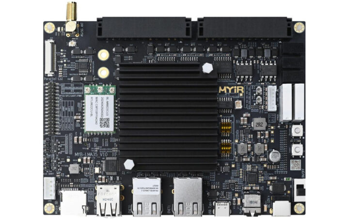


")