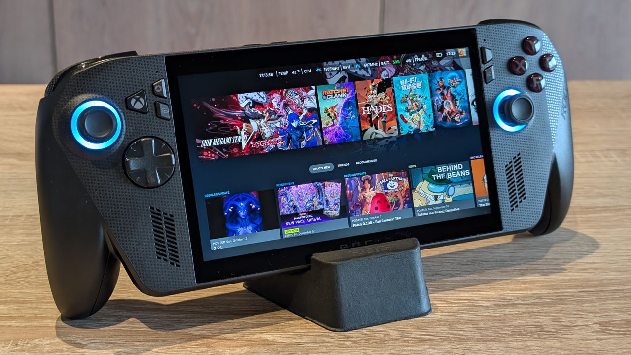
FreshRSS

Normální zobrazení

Jsou dostupné nové články, klikněte pro obnovení stránky.
PředevčíremHlavní kanál
  • ✇AnandTech
  • G.Skill Intros Low Latency DDR5 Memory Modules: CL30 at 6400 MT/s
    G.Skill on Tuesday introduced its ultra-low-latency DDR5-6400 memory modules that feature a CAS latency of 30 clocks, which appears to be the industry's most aggressive timings yet for DDR5-6400 sticks. The modules will be available for both AMD and Intel CPU-based systems. With every new generation of DDR memory comes an increase in data transfer rates and an extension of relative latencies. While for the vast majority of applications, the increased bandwidth offsets the performance impact of
     

G.Skill Intros Low Latency DDR5 Memory Modules: CL30 at 6400 MT/s

13. Srpen 2024 v 22:45

G.Skill on Tuesday introduced its ultra-low-latency DDR5-6400 memory modules that feature a CAS latency of 30 clocks, which appears to be the industry's most aggressive timings yet for DDR5-6400 sticks. The modules will be available for both AMD and Intel CPU-based systems.

With every new generation of DDR memory comes an increase in data transfer rates and an extension of relative latencies. While for the vast majority of applications, the increased bandwidth offsets the performance impact of higher timings, there are applications that favor low latencies. However, shrinking latencies is sometimes harder than increasing data transfer rates, which is why low-latency modules are rare.

Nonetheless, G.Skill has apparently managed to cherry-pick enough DDR5 memory chips and build appropriate printed circuit boards to produce DDR5-6400 modules with CL30 timings, which are substantially lower than the CL46 timings recommended by JEDEC for this speed bin. This means that while JEDEC-standard modules have an absolute latency of 14.375 ns, G.Skill's modules can boast a latency of just 9.375 ns – an approximately 35% decrease.

G.Skill's DDR5-6400 CL30 39-39-102 modules have a capacity of 16 GB and will be available in 32 GB dual-channel kits, though the company does not disclose voltages, which are likely considerably higher than those standardized by JEDEC.

The company plans to make its DDR5-6400 modules available both for AMD systems with EXPO profiles (Trident Z5 Neo RGB and Trident Z5 Royal Neo) and for Intel-powered PCs with XMP 3.0 profiles (Trident Z5 RGB and Trident Z5 Royal). For AMD AM5 systems that have a practical limitation of 6000 MT/s – 6400 MT/s for DDR5 memory (as this is roughly as fast as AMD's Infinity Fabric can operate at with a 1:1 ratio), the new modules will be particularly beneficial for AMD's Ryzen 7000 and Ryzen 9000-series processors.

G.Skill notes that since its modules are non-standard, they will not work with all systems but will operate on high-end motherboards with properly cooled CPUs.

The new ultra-low-latency memory kits will be available worldwide from G.Skill's partners starting in late August 2024. The company did not disclose the pricing of these modules, but since we are talking about premium products that boast unique specifications, they are likely to be priced accordingly.

Data Memory-Dependent Prefetchers Pose SW Security Threat By Breaking Cryptographic Implementations

A technical paper titled “GoFetch: Breaking Constant-Time Cryptographic Implementations Using Data Memory-Dependent Prefetchers” was presented at the August 2024 USENIX Security Symposium by researchers at University of Illinois Urbana-Champaign, University of Texas at Austin, Georgia Institute of Technology, University of California Berkeley, University of Washington, and Carnegie Mellon University.

Abstract:

“Microarchitectural side-channel attacks have shaken the foundations of modern processor design. The cornerstone defense against these attacks has been to ensure that security-critical programs do not use secret-dependent data as addresses. Put simply: do not pass secrets as addresses to, e.g., data memory instructions. Yet, the discovery of data memory-dependent prefetchers (DMPs)—which turn program data into addresses directly from within the memory system—calls into question whether this approach will continue to remain secure.

This paper shows that the security threat from DMPs is significantly worse than previously thought and demonstrates the first end-to-end attacks on security-critical software using the Apple m-series DMP. Undergirding our attacks is a new understanding of how DMPs behave which shows, among other things, that the Apple DMP will activate on behalf of any victim program and attempt to “leak” any cached data that resembles a pointer. From this understanding, we design a new type of chosen-input attack that uses the DMP to perform end-to-end key extraction on popular constant-time implementations of classical (OpenSSL Diffie-Hellman Key Exchange, Go RSA decryption) and post-quantum cryptography (CRYSTALS-Kyber and CRYSTALS-Dilithium).”

Find the technical paper here. Published August 2024.

Chen, Boru, Yingchen Wang, Pradyumna Shome, Christopher W. Fletcher, David Kohlbrenner, Riccardo Paccagnella, and Daniel Genkin. “GoFetch: Breaking constant-time cryptographic implementations using data memory-dependent prefetchers.” In Proc. USENIX Secur. Symp, pp. 1-21. 2024.

Further Reading
Chip Security Now Depends On Widening Supply Chain
How tighter HW-SW integration and increasing government involvement are changing the security landscape for chips and systems.


The post Data Memory-Dependent Prefetchers Pose SW Security Threat By Breaking Cryptographic Implementations appeared first on Semiconductor Engineering.

  • ✇Recent Questions - Game Development Stack Exchange
  • Why does this function cause memory leaks?Leo
    I'm trying to make a pickup and drop script by myself and every time the game calls the pickup function, it seemed to cause memory leaks and freezes the game for few seconds. After those few seconds, the items does get picked up but the fps drops significant and the drop function seems to do fine. *Attached to the Item holder using UnityEngine; public class PickupController : MonoBehaviour { public GameObject itemHolder; public bool slotFull; private GameObject currentObject
     

Why does this function cause memory leaks?

I'm trying to make a pickup and drop script by myself and every time the game calls the pickup function, it seemed to cause memory leaks and freezes the game for few seconds. enter image description here enter image description here enter image description here enter image description here 200 -> 130 After those few seconds, the items does get picked up but the fps drops significant and the drop function seems to do fine.
After getting picked up hierarchy

*Attached to the Item holder

using UnityEngine;

public class PickupController : MonoBehaviour
{
    public GameObject itemHolder;

    public bool slotFull;

    private GameObject currentObject;

    private IPickable pickupScript;

    public void PickUp(GameObject pickupObject)
    {

        if (pickupObject == null)
        {
            Debug.LogError("Pickup Object is null");
            return;
        }

        slotFull = true;
        currentObject = pickupObject;
        pickupScript = pickupObject.GetComponentInChildren<IPickable>(); //I'm trying to get the WheelRange.cs script

        Debug.Log(pickupObject.gameObject.name);

        if (pickupScript == null)
        {
            Debug.LogError("pickupScript is null.");
            return;
        }


        currentObject.transform.SetParent(itemHolder.transform);

        pickupScript.OnItemPickup();

        currentObject.transform.localPosition = Vector3.zero;
        currentObject.transform.localRotation = Quaternion.identity;
    }

    public void Drop()
    {
        slotFull = false;
        currentObject.transform.SetParent(null); //Removes the parent
        pickupScript.OnItemDrop();
    }
}

*Attached to WheelRange gameobject

using UnityEngine;

public class WheelRange : MonoBehaviour, IPickable
{
    
    [SerializeField] private Canvas canvas;
    [SerializeField] private BoxCollider boxCollider;
    [SerializeField] private PickupController pickupScript;
    private GameObject parentObject;
    private bool beingUsed;
    private float distToGround;


    void Start()
    {
        beingUsed = false;
        canvas.gameObject.SetActive(false);
        parentObject = this.transform.parent.gameObject; //Gets the actual wheel gameobject
        distToGround = boxCollider.bounds.extents.y;
    }
    public void OnItemPickup()
    {
        beingUsed = true;
        pickupScript.PickUp(parentObject);

        boxCollider.gameObject.SetActive(false);
        canvas.gameObject.SetActive(false);
        
    }

    public void OnItemDrop()
    {
        beingUsed = false;
        boxCollider.gameObject.SetActive(true);
        
    }


    //Rest of these functions probably doesn't apply to the error
    bool IsGrounded()
    {
        return Physics.Raycast(parentObject.transform.position, Vector3.down, distToGround + 0.1f);

    }

    void OnTriggerEnter(Collider other)
    {
        if (other.gameObject.tag == "Player") canvas.gameObject.SetActive(true);
    }

    void OnTriggerExit(Collider other)
    {
        if (other.gameObject.tag == "Player") canvas.gameObject.SetActive(false);
    }
}

The interface

public interface IPickable
{
    void OnItemPickup();

    void OnItemDrop();
}

New PS5 SSD Will Let You Store All Of The Games For Just $1,000

20. Srpen 2024 v 19:00

Few PlayStation 5 owners dare to dream of a day when all of their games can be downloaded and installed on the console at the same time. But thanks to a new 8TB SSD, that dream is becoming a little more real, and very expensive.

Read more...

  • ✇Semiconductor Engineering
  • Are You Ready For HBM4? A Silicon Lifecycle Management (SLM) PerspectiveFaisal Goriawalla
    Many factors are driving system-on-chip (SoC) developers to adopt multi-die technology, in which multiple dies are stacked in a three-dimensional (3D) configuration. Multi-die systems may make power and thermal issues more complex, and they have required major innovations in electronic design automation (EDA) implementation and test tools. These challenges are more than offset by the advantages of over traditional 2D designs, including: Reducing overall area Achieving much higher pin densities
     

Are You Ready For HBM4? A Silicon Lifecycle Management (SLM) Perspective

Many factors are driving system-on-chip (SoC) developers to adopt multi-die technology, in which multiple dies are stacked in a three-dimensional (3D) configuration. Multi-die systems may make power and thermal issues more complex, and they have required major innovations in electronic design automation (EDA) implementation and test tools. These challenges are more than offset by the advantages of over traditional 2D designs, including:

  • Reducing overall area
  • Achieving much higher pin densities
  • Reusing existing proven dies
  • Mixing heterogeneous die technologies
  • Quickly creating derivative designs for new applications

One of the most common uses of multi-die design is the interconnection of memory stacks and processors such as CPUs and GPUs. High Bandwidth Memory (HBM) is a standard interface specifically for 3D-stacked DRAM dies. It was defined by the JEDEC Solid State Technology Association in 2013, followed by HBM2 in 2016 and HBM3 in 2022. Many multi-die projects have used this standard for caches in advanced CPUs and other system-on-chip (SoC) designs used in high-end applications such as data centers, high-performance computing (HPC), and artificial intelligence (AI) processing.

Fig. 1: Example of a current HBM-based SoC.

JEDEC recently announced that it is nearing completion of HBM4 and published preliminary specifications. HBM4 has been developed to enhance data processing rates while maintaining higher bandwidth, lower power consumption, and increased capacity per die/stack. The initial agreement calls for speed bins up to 6.4 Gbps, although this will increase as memory vendors develop new chips and refine the technology. This speed will benefit applications that require efficient handling of large datasets and complex calculations.

HBM4 is introducing a doubled channel count per stack over HBM3. The new version of the standard features a 2048-bit memory interface, as compared to 1024 bits in previous versions, as shown in figure 1. This intent is to double the number of bits without increasing the footprint of HBM memory stacks, thus doubling the interconnection density as well.

Different memory configurations will require various interposers to accommodate the differing footprints. HBM4 will specify 24 Gb and 32 Gb layers, with options for supporting 4-high, 8-high, 12-high and 16-high TSV stacks. As an example configuration, a 16-high based on 32 Gb layers will offer a capacity of 64 GB, which means that a processor with four memory modules can support 256 GB of memory with a peak bandwidth of 6.56 TB/s using an 8,192-bit interface.

The move from HBM3 to HBM4 will require further evolution in multi-die support across a wide range of EDA tools. The 2048-bit memory interface requires a significant increase in the number of through-silicon vias (TSVs) routed through a memory stack. This will mean shrinking the external bump pitch as the total number of micro bumps increases significantly. In addition, support for 16-high TSV stacks brings new complexity in wiring up an even larger number of DRAM dies without defects.

Test challenges are likely to be a dominant part of the transition. Any signal integrity issues after assembly and multi-die packaging become more difficult to diagnose and debug since probing is not feasible. Further, some defects may marginally pass production/manufacturing test but subsequently fail in the field. Thus, test of the future HBM4-based subsystem needs to be accomplished not just at production test but also in-system to account for aging-related defects.

Being able to monitor real-time data during mission mode operation in the field is greatly preferable to having to take the system offline for unplanned service. This “predictive maintenance” allows the end user to be proactive rather than reactive. HBM provides capabilities for in-system repair, for example swapping out a bad lane. Even if a defect requires physical hardware repair, detecting it before system failure enables scheduled maintenance rather than unplanned downtime.

As shown in figure 1, HBM systems typically have a base die that includes an HBM controller, a basic/fixed test engine provided by the DRAM vendor, and Direct Access (DA) ports. The new industry trend is for the base die to be manufactured on a standard logic process rather than the DRAM process. The SoC designer should include in the base die a flexible built-in self-test (BIST) engine that allows different algorithms to be used to trade off high coverage versus test time depending on the scenario.

This engine must be programmable to handle different latencies, address ranges, and timing of test operations that vary across DRAM vendors. It may also need to support post-package repair (PPR) for HBM DRAM to delay any “truck roll-out” for in-field service. The diagnostics performed by the BIST engine must be precise, showing the failing bank, row address, column address, etc. if there is a defect detected in the DRAM stack. Figure 2 shows an example.

Fig. 2: Example fault diagnosis for HBM stack.

As an industry leader in multi-die EDA and IP solutions, Synopsys provides all the technology needed for HBM manufacturing yield optimization and in-field silicon health monitoring. Signal Integrity Monitors (SIMs) are embedded in physical layer (PHY) IP blocks for on-demand signal quality measurement for interconnects. This allows users to create 1D eye diagrams for interconnect signals during both production test and in-field operation. SIMs measure timing margins, enable HBM lane test/repair, and mitigate against silent data corruption (SDC), part of an effective silicon lifecycle management (SLM) solution.

Synopsys SMS ext-RAM is a programmable and synthesizable engine that performs test, repair, and diagnostics for memory systems, including HBM. SMS ext-RAM ensures high test coverage and supports power-on self-test (POST) with the flexibility to run custom memory algorithms in-field. As shown in figure 2, it detects a wide range of defects in memory dies, including stuck-at faults, read destructive faults, write destructive faults, deceptive read destructive faults, and row hammering.

A real world case study of a project using HBM with the Synopsys solutions is available. These solutions are scaling to support the emerging HBM4 standard, ensuring continued success.

The post Are You Ready For HBM4? A Silicon Lifecycle Management (SLM) Perspective appeared first on Semiconductor Engineering.

  • ✇NekoJonez's Gaming Blog
  • First Impression: Another Code: Recollection (Switch) ~ The Remembering Of A RemakeNekoJonez
    Nintendo.co.uk microsite – Wikipedia page Next year, I’ll be blogging for 15 years. I have taken a look at quite a lot of games. Now, if you go back to the start of this blog, you might notice that I only started in May 2013. The three years before that, I wrote a personal life blog in my native language. I have since deleted that for personal reasons and started blogging in English in 2013. On my Dutch blog, I wrote an article about Another Code – Two Memories, but I haven’t written one
     

First Impression: Another Code: Recollection (Switch) ~ The Remembering Of A Remake

Od: NekoJonez
10. Březen 2024 v 15:12

Nintendo.co.uk micrositeWikipedia page

Next year, I’ll be blogging for 15 years. I have taken a look at quite a lot of games. Now, if you go back to the start of this blog, you might notice that I only started in May 2013. The three years before that, I wrote a personal life blog in my native language. I have since deleted that for personal reasons and started blogging in English in 2013. On my Dutch blog, I wrote an article about Another Code – Two Memories, but I haven’t written one for my English blog. Yet, I have mentioned it in 2014 in a top 25 list of my favorite DS games of all time. I have written an article on the Wii sequel called Another Code: R – A Journey Into Lost Memories in 2013. While my old articles aren’t up to my personal standards anymore, I still leave them up to see the growth I have gone through over the years. Now, these two titles became classics in my eyes. When Cing went under, I didn’t hold up hope of these games ever seeing a sequel or a remake. But, we got a big surprise this year. Suddenly, both games were coming to the Nintendo Switch and not only that, they were remade from the ground up. Did these two games grow like I did in my writing, or is it something that should be better left to the past? Well, that’s what I’m going to discover with you in this article. Feel free to leave a comment in the comment section with your thoughts and/or opinions on the game and/or the content of the article, but now, let’s dive right in.

Editorial note: shameless self-promotion: if you want to see me and my buddy Klamath playing through this title… We started streaming it. So, more opinions can be found in the streams. Here is a link to the playlist.

The Remembering Of A Remake

In this game, we follow the adventures of Ashley Mizuki Robins. In the first part of the game, Ashley got a letter from her presumed dead father to come to Blood Edward island to meet him on the day right before her 14th birthday. On that journey, she meets a ghost named D, who has lost his memories.

In the second part of the game, we fast-forward two years. Ashley takes a camping trip to a lake. When she arrives at lake Juliet, she gets flashbacks from when she was very little. Not only that, she meets a young boy whose father wanted to build a holiday resort at that lake but was blamed for the pollution of the lake.

Since this game is a point-and-click game and is quite story depended, I’m not going to talk more about the story than the two small blurbs above. In terms of the story, this game tells a very heartfelt story with very nice life lessons. The writing in this game is extremely well done. The build up towards the ending of the story is very natural and stays true to the themes of the game. The biggest theme in this game is memories and history. Overall, this game is quite relaxing, and the story is never really in a rush to move forward.

New in this version is that there is voice acting. While not the whole game is voice acted, most of it is and the non voice acted scenes have little grunts and vocalizations to indicate the emotions of what’s being told. I have to say that the voice acting in this game is fantastic. I wish the voice actors of this game had more of an online presence, since I had a hard time finding other works by these voice actors. The fact that these voice actors didn’t really promote that they worked on this game on their socials is a shame.

The voice acting in this game brings so much charm to the game. For this article, I replayed parts of the original DS and Wii game and I kept hearing those characters talk in the voice of the remakes. They fit the characters like a glove, which is a hard thing to do since when you have voiceless characters… Everybody has their voice in their head, and that doesn’t always match up with the official voice acting.

Now, in terms of differences between the original games and this remake… There are quite a lot of things. On the Cing wiki, there is a long list of changes. But I would highly advise you don’t read that before you finished the game. Since, it contains a lot of spoilers. I can say this without spoiling anything. The list of changes on the game article page has no real spoilers. If you haven’t played the originals, you won’t really notice a lot of the changes. Especially because most of the changes are done to improve the flow of the game and the story. Other changes have been done because some puzzles used the special features of the Nintendo DS or the Nintendo Wii in unique ways.

Arc System Works worked together with several members of the original development team, and I have to say that it really feels like this is the definitive way to experience these stories. Both stories now flow into each other, and it feels more like one big story. If you didn’t know better, you could think it’s just one huge game with those major chapters. They have done an amazing job of translating the story into a modern area without destroying the original messages and atmosphere of the story.

Fuzzy memories make imperfections

In terms of visuals, this game goes for a cel shaded look. This makes the remake of the original DS game look more in line with the Wii title. In the original DS game, the game was played as a top-down puzzle game, with some moments you could see a 2D scene that you could explore.

Visually, this game is quite detailed and looks amazing. Yet, I have noticed some rough models here and there. A book here, a window there. Some of them really stick out like a sore thumb. Now, I might be very critical on these things since I review games as a hobby. But let me tell you this as well. Overall, this game looks amazing. Timeless even. There are only a handful of objects that could use some touching up.

I have the same opinion on the animations. Overall, the animations are fantastic. Seeing the first game in 3D was breathtaking. It brought the game to life in such a different way, and I’m all for it. There were a few stiff animations, but if you aren’t looking for them, I can guarantee you that you won’t notice most of them. I especially love the comic book style cutscenes where the characters speaking go inside their own square next to each other. The animations in these cutscenes add some charm to this game, it makes the more relaxing nature of this game shine even brighter.

The controls of this game are excellent. Sometimes the motion control puzzles are a little bit wonky, but overall they work perfectly. The only thing I really don’t like is how, by the press of a button, you can see the orientation of Ashley. Now, what do I dislike about this? Well, it has a sort of build in walkthrough attached to it. This is something that’s too easily accessible, and I have pressed the button too many times.

Something I’m mixed about is how the additional lore spots are now somewhat easier to find. In the original DS game, you could find special cartridges with additional story lore on them. In this game, the hiding spot is located on your map. So, if you have missed one, you can quickly see on your map in which room you need to look. Now, some of them are hidden in very tricky places. During the stream, I have seen Klamath walk past two of them several times. If you want all the additional lore, you will have to keep your eyes peeled.

If you have played any point-and-click adventure game, you’ll know what to expect here. Personally, I compare this game quite a lot to Broken Sword 3, but without the platforming. You can explore the environment, and you have to solve various puzzles. Something unique is that you can also take pictures. And let me tell you, keep every mechanic the game teaches you in mind. The fact you can take pictures is something that is going to be quite helpful during the solving of the puzzles.

The only complaint I have is that solving some puzzles have a bit too much menu work involved. I especially remember one puzzle in the first part of the game where you have to weigh coins. Instead of them being all five on the table, you have to take them from your inventory each and every time. And the annoying part is that the last two you used, move to the last spot in your inventory. There are a handful of puzzles where some quality of life improvements would be very welcome.

Relaxing with puzzles

There are some amazing new features in this game as well. One of my favorite things is that you can access a big board where all the relationships between the characters are mapped out. Not only that, when you open the profile, you can read a small note about them. If you click on Ashley’s profile, you will read a small hint on what to do next. So, if you put this game down for a while, you can catch yourself up quite quickly.

Also, something I adore is the attention to detail in this game. For example, in one of the puzzles, Ashley digs into a building blocks box. After she found what she was looking for, you will notice a small building she built next to the box with the blocks she took out. There are various other moments like this, and it adds to the charm and realism of this game quite a lot.

The more relaxing nature of this game not only comes through the visuals and gameplay, but also through the music. The music in this game is a rather calming and relaxing soundtrack. The main motive is piano through the whole soundtrack. Other major instruments are violin and acoustic guitar. The soundtracks fit this game like a glove. Now, it is tense when it needs to be, but it never steps out of its lane. It keeps being that relaxing soundtracks that brings this game more to life, and I have no complaints about it.

The biggest strength of this game is the charm of it all. The writing, the music, the sound effects, the puzzles… It all flows together so well. While the game is only roughly 15 hours long, if you know what you are doing, it’s a very enjoyable time to play through. In this remake, the game also auto saves now but outside of cutscenes, you can save at any time in 15 different save slots.

Currently, I’m over midway in the second part of the game and I have been enjoying it quite a lot. While the game has it’s minor shortcomings like some rough object models and some annoying menu’ing during puzzles… I’m falling in love with these titles all over again. If you would ask me if the remakes or the originals are better, I’d have to say both. Both versions still have their charm but if you want to experience both these titles, I’d really advice to go for the Switch version. Since, it brings both titles together in a lot better way.

I mostly have minor complaints about these remakes. Like how silly it is that you can only have ten pictures saved and deleting them is a bit too fincky. But overall, the issues I have with this game are mostly minor. Maybe a bit more time in the oven or a polishing patch will bring this game to perfection.

A lot of other reviewers are giving this game lower marks since it’s slower paced or it’s a remake of a rather obscure duology. I personally disagree with these lower scores. These two games deserve another chance in the lime light since they are quite amazing games. I personally don’t mind the slower paced gameplay, since it’s refreshing to be able to wind down with a slower game. On top of that, if you look at the care the developers put into remaking this game and bringing it to modern audiences while not chaging too much to alienate fans of the original is such a fine line to walk on… And they never fell off that line in my opinion.

I can totally understand that this game isn’t everybody’s cup of tea. But, the complaints that this game is linear and doesn’t have a lot of replay value, I find ridiculous. I mean, does every game need to have a lot of replay value and let you explore a wide open world? No, it’s okay to play a game where you need to go from point A to B. It’s okay that the story looses some of it’s charm because you know how it’s going to end. It’s how that experience impacts you, that’s what matters.

The reason why I’m so happy to see remakes of these DS and Wii titles is because we now have remakes of amazing titles like this one and Ghost Trick for example. Now, because these two games have been remade, I’m holding out hope that Cing’s other titles like the amazing Hotel Dusk and it’s sequels are being remade as well. And if they are, I hope the same team is working on them since the love and care they placed into remaking these two titles is amazing.

I remember Klamath’s reaction when I suggested this game for streaming. He was worried that it was going to have low numbers and not a lot of interest. But, after our first stream, he started calling this game a hidden gem. I mean, if this game can have that kind of an impact on somebody who loves point-and-click games and the fact that we had a very high number of viewers watching our streams, it must mean something.

This game has a lot of impact and I hope that others who enjoy puzzle, adventure and/or point-and-click games give this game a chance. It’s something different especially since it’s slower paced but if you let it take you by the hand and if you walk along the journey, you won’t regret the powerful journey you are going on. It’s a journey that will stick with you and sometimes a memory will pop back into your head. You’ll remember the fun and relaxing times you had with this game. While the game isn’t perfect, the positives far outweigh the negatives and it’s one of those games where going along with the ride is the most important. Since, the ride of this game is one of the best point-and-click games I have ever played.

And with that said, I have said everything I wanted to say about this game for now. I want to thank you so much for reading this article and I hope you enjoyed reading it as much as I enjoyed writing it. I’m curious to hear what you thought about this game and/or the content of this article. So, feel free to leave a comment in the comment section down below. I also hope to welcome you in another article, but until then have a great rest of your day and take care.

  • ✇AnandTech
  • Samsung Shrinks LPDDR5X Chips by 9%, Now Just 0.65mm Thick
    Samsung is announcing today that it has begun mass production of 12 GB and 16 GB LPDDR5X modules in the industry's thinnest package. Samsung's shrunken memory packages measure approximately 0.65 mm in thickness, making them 0.06 mm (~9%) thinner than standard LPDDR5X packages. The company expects the new DRAM devices to be used to make for thinner smartphones, or improve their performance by enabling better airflow inside. According to the company's press release, Samsung achieved this ultra-th
     

Samsung Shrinks LPDDR5X Chips by 9%, Now Just 0.65mm Thick

6. Srpen 2024 v 01:00

Samsung is announcing today that it has begun mass production of 12 GB and 16 GB LPDDR5X modules in the industry's thinnest package. Samsung's shrunken memory packages measure approximately 0.65 mm in thickness, making them 0.06 mm (~9%) thinner than standard LPDDR5X packages. The company expects the new DRAM devices to be used to make for thinner smartphones, or improve their performance by enabling better airflow inside.

According to the company's press release, Samsung achieved this ultra-thin design by employing new packaging methods, such as optimized printed circuit boards (PCBs) and epoxy molding compound (EMC). Additionally, an optimized back-lapping process was used to further reduce the height of the packages. The newly developed DRAM packages are not only thinner by 9% compared to previous models but also offer a 21.2% improvement in heat resistance. 

Thinner LPDDR5X packaging help enhance airflow within smartphones, significantly improving thermal management, which means higher performance and longer battery life. Also, better thermal management help to prolong device's lifespan.

"Samsung's LPDDR5X DRAM sets a new standard for high-performance on-device AI solutions, offering not only superior LPDDR performance but also advanced thermal management in an ultra-compact package," said YongCheol Bae, Executive Vice President of Memory Product Planning at Samsung Electronics. "We are committed to continuous innovation through close collaboration with our customers, delivering solutions that meet the future needs of the low-power DRAM market."

While Samsung's thinner LPDDR5X DRAM packages contribute to making smartphones slimmer, they are just one part of the overall design strategy. Other components, such as thinner protective glass, PCBs, and batteries, play considerably more significant roles in reducing device thickness. Meanwhile, the primary benefit of these new memory modules may be in improving airflow inside smartphones.

Samsung is looking to further expand its LPDDR5X product lineups by developing even more compact packages, including 6-layer 24 GB and 8-layer 32 GB modules. Specific details about the thickness of these future memory modules have not yet been disclosed, though making high-capacity DRAMs thinner in general is an important thing.

  • ✇AnandTech
  • JEDEC Plans LPDDR6-Based CAMM, DDR5 MRDIMM Specifications
    Following a relative lull in the desktop memory industry in the previous decade, the past few years have seen a flurry of new memory standards and form factors enter development. Joining the traditional DIMM/SO-DIMM form factors, we've seen the introduction of space-efficient DDR5 CAMM2s, their LPDDR5-based counterpart the LPCAMM2, and the high-clockspeed optimized CUDIMM. But JEDEC, the industry organization behind these efforts, is not done there. In a press release sent out at the start of th
     

JEDEC Plans LPDDR6-Based CAMM, DDR5 MRDIMM Specifications

24. Červenec 2024 v 01:00

Following a relative lull in the desktop memory industry in the previous decade, the past few years have seen a flurry of new memory standards and form factors enter development. Joining the traditional DIMM/SO-DIMM form factors, we've seen the introduction of space-efficient DDR5 CAMM2s, their LPDDR5-based counterpart the LPCAMM2, and the high-clockspeed optimized CUDIMM. But JEDEC, the industry organization behind these efforts, is not done there. In a press release sent out at the start of the week, the group announced that it is working on standards for DDR5 Multiplexed Rank DIMMs (MRDIMM) for servers, as well as an updated LPCAMM standard to go with next-generation LPDDR6 memory.

Just last week Micron introduced the industry's first DDR5 MRDIMMs, which are timed to launch alongside Intel's Xeon 6 server platforms. But while Intel and its partners are moving full steam ahead on MRDIMMs, the MRDIMM specification has not been fully ratified by JEDEC itself. All told, it's not unusual to see Intel pushing the envelope here on new memory technologies (the company is big enough to bootstrap its own ecosystem). But as MRDIMMs are ultimately meant to be more than just a tool for Intel, a proper industry standard is still needed – even if that takes a bit longer.

Under the hood, MRDIMMs continue to use DDR5 components, form-factor, pinout, SPD, power management ICs (PMICs), and thermal sensors. The major change with the technology is the introduction of multiplexing, which combines multiple data signals over a single channel. The MRDIMM standard also adds RCD/DB logic in a bid to boost performance, increase capacity of memory modules up to 256 GB (for now), shrink latencies, and reduce power consumption of high-end memory subsystems. And, perhaps key to MRDIMM adoption, the standard is being implemented as a backwards-compatible extension to traditional DDR5 RDIMMs, meaning that MRDIMM-capable servers can use either RDIMMs or MRDIMMs, depending on how the operator opts to configure the system.

The MRDIMM standard aims to double the peak bandwidth to 12.8 Gbps, increasing pin speed and supporting more than two ranks. Additionally, a "Tall MRDIMM" form factor is in the works (and pictured above), which is designed to allow for higher capacity DIMMs by providing more area for laying down memory chips. Currently, ultra high capacity DIMMs require using expensive, multi-layer DRAM packages that use through-silicon vias (3DS packaging) to attach the individual DRAM dies; a Tall MRDIMM, on the other hand, can just use a larger number of commodity DRAM chips. Overall, the Tall MRDIMM form factor enables twice the number of DRAM single-die packages on the DIMM.

Meanwhile, this week's announcement from JEDEC offers the first significant insight into what to expect from LPDDR6 CAMMs. And despite LPDDR5 CAMMs having barely made it out the door, some significant shifts with LPDDR6 itself means that JEDEC will need to make some major changes to the CAMM standard to accommodate the newer memory type.


JEDEC Presentation: The CAMM2 Journey and Future Potential

Besides the higher memory clockspeeds allowed by LPDDR6 – JEDEC is targeting data transfer rates of 14.4 GT/s and higher – the new memory form-factor will also incorporate an altogether new connector array. This is to accommodate LPDDR6's wider memory bus, which sees the channel width of an individual memory chip grow from 16-bits wide to 24-bits wide. As a result, the current LPCAMM design, which is intended to match the PC standard of a cumulative 128-bit (16x8) design needs to be reconfigured to match LPDDR6's alterations.

Ultimately, JEDEC is targeting a 24-bit subhannel/48-bit channel design, which will result in a 192-bit wide LPCAMM. While the LPCAMM connector itself is set to grow from 14 rows of pins to possibly as high as 20. New memory technologies typically require new DIMMs to begin with, so it's important to clarify that this is not unexpected, but at the end of the day it means that the LPCAMM will be undergoing a bigger generational change than what we usually see.

JEDEC is not saying at this time when they expect either memory module standard to be completed. But with MRDIMMs already shipping for Intel systems – and similar AMD server parts due a bit later this year – the formal version of that standard should be right around the corner. Meanwhile, LPDDR6 CAMMs will be a bit farther out, particularly as the memory standard itself is still under development.

  • ✇AnandTech
  • Samsung Validates LPDDR5X Running at 10.7 GT/sec with MediaTek's Dimensity 9400 SoC
    Samsung has successfully validated its new LPDDR5X-10700 memory with MediaTek's upcoming Dimensity platform. At present, 10.7 GT/s is the highest performing speed grade of LPDDR5X DRAM slated to be released this year, so the upcoming Dimensity 9400 system-on-chip will get the highest memory bandwidth available for a mobile application processor. The verification process involved Samsung's 16 GB LPDDR5X package and MediaTek's soon-to-be-announced Dimensity 9400 SoC for high-end 5G smartphones. U
     

Samsung Validates LPDDR5X Running at 10.7 GT/sec with MediaTek's Dimensity 9400 SoC

17. Červenec 2024 v 14:00

Samsung has successfully validated its new LPDDR5X-10700 memory with MediaTek's upcoming Dimensity platform. At present, 10.7 GT/s is the highest performing speed grade of LPDDR5X DRAM slated to be released this year, so the upcoming Dimensity 9400 system-on-chip will get the highest memory bandwidth available for a mobile application processor.

The verification process involved Samsung's 16 GB LPDDR5X package and MediaTek's soon-to-be-announced Dimensity 9400 SoC for high-end 5G smartphones. Usage of LPDDR5X-10700 provides a memory bandwidth of 85.6 GB/second over a 64-bit interface, which will be available for bandwidth-hungry applications like graphics and generative AI.

"Working together with Samsung Electronics has made it possible for MediaTek's next-generation Dimensity chipset to become the world's first to be validated at LPDDR5X operating speeds up to 10.7Gbps, enabling upcoming devices to deliver AI functionality and mobile performance at a level we have never seen before," said JC Hsu, Corporate Senior Vice President at MediaTek. "This updated architecture will make it easier for developers and users to leverage more AI capabilities and take advantage of more features with less impact on battery life."

Samsung's LPDDR5X 10.7 GT/s memory in made on the company's 12nm-class DRAM process technology and is said to provide a more than 25% improvement in power efficiency over previous-generation LPDDR5X, in addition to extra performance. This will positively affect improved user experience, including enhanced on-device AI capabilities, such as faster voice-to-text conversion, and better quality graphics.

Overall, the two companies completed this process in just three months. Though it remains to be seen when smartphones based on the Dimensity 9400 application processor and LPDDR5X memory are set to be available on the market, as MediaTek has not yet even formally announced the SoC itself.

"Through our strategic cooperation with MediaTek, Samsung has verified the industry's fastest LPDDR5X DRAM that is poised to lead the AI smartphone market," said YongCheol Bae, Executive Vice President of Memory Product Planning at Samsung Electronics. "Samsung will continue to innovate through active collaboration with customers and provide optimum solutions for the on-device AI era."

  • ✇AnandTech
  • Micron Expands Datacenter DRAM Portfolio with MR-DIMMs
    The compute market has always been hungry for memory bandwidth, particularly for high-performance applications in servers and datacenters. In recent years, the explosion in core counts per socket has further accentuated this need. Despite progress in DDR speeds, the available bandwidth per core has unfortunately not seen a corresponding scaling. The stakeholders in the industry have been attempting to address this by building additional technology on top of existing widely-adopted memory stan
     

Micron Expands Datacenter DRAM Portfolio with MR-DIMMs

16. Červenec 2024 v 15:10

The compute market has always been hungry for memory bandwidth, particularly for high-performance applications in servers and datacenters. In recent years, the explosion in core counts per socket has further accentuated this need. Despite progress in DDR speeds, the available bandwidth per core has unfortunately not seen a corresponding scaling.

The stakeholders in the industry have been attempting to address this by building additional technology on top of existing widely-adopted memory standards. With DDR5, there are currently two technologies attempting to increase the peak bandwidth beyond the official speeds. In late 2022, SK hynix introduced MCR-DIMMs meant for operating with specific Intel server platforms. On the other hand, JEDEC - the standards-setting body - also developed specifications for MR-DIMMs with a similar approach. Both of them build upon existing DDR5 technologies by attempting to combine multiple ranks to improve peak bandwidth and latency.

How MR-DIMMs Work

The MR-DIMM standard is conceptually simple - there are multiple ranks of memory modules operating at standard DDR5 speeds with a data buffer in front. The buffer operates at 2x the speed on the host interface side, allowing for essentially double the transfer rates. The challenges obviously lie in being able to operate the logic in the host memory controller at the higher speed and keeping the power consumption / thermals in check.

The first version of the JEDEC MR-DIMM standard specifies speeds of 8800 MT/s, with the next generation at 12800 MT/s. JEDEC also has a clear roadmap for this technology, keeping it in sync with the the improvements in the DDR5 standard.

Micron MR-DIMMs - Bandwidth and Capacity Plays

Micron and Intel have been working closely in the last few quarters to bring their former's first-generation MR-DIMM lineup to the market. Intel's Xeon 6 Family with P-Cores (Granite Rapids) is the first platform to bring MR-DIMM support at 8800 MT/s on the host side. Micron's standard-sized MR-DIMMs (suitable for 1U servers) and TFF (tall form-factor) MR-DIMMs (for 2U+ servers) have been qualified for use with the same.

The benefits offered by MR-DIMMs are evident from the JEDEC specifications, allowing for increased data rates and system bandwidth, with improvements in latency. On the capacity side, allowing for additional ranks on the modules has enabled Micron to offer a 256 GB capacity point. It must be noted that some vendors are also using TSV (through-silicon vias) technology to to increase the per-package capacity at standard DDR5 speeds, but this adds additional cost and complexity that are largely absent in the MR-DIMM manufacturing process.

The tall form-factor (TFF) MR-DIMMs have a larger surface area compared to the standard-sized ones. For the same airflow configuration, this allows the DIMM to have a better thermal profile. This provides benefits for energy efficiency as well by reducing the possibility of thermal throttling.

Micron is launching a comprehensive lineup of MR-DIMMs in both standard and tall form-factors today, with multiple DRAM densities and speed options as noted above.

MRDIMM Benefits - Intel Granite Rapids Gets a Performance Boost

Micron and Intel hosted a media / analyst briefing recently to demonstrate the benefits of MR-DIMMs for Xeon 6 with P-Cores (Granite Rapids). Using a 2P configuration with 96-core Xeon 6 processors, benchmarks for different workloads were processed with both 8800 MT/s MR-DIMMs and 6400 MT/s RDIMMs. The chosen workloads are particularly notorious for being limited in performance by memory bandwidth.

OpenFOAM is a widely-used CFD workload that benefits from MR-DIMMs. For the same memory capacity, the 8800 MT/s MR-DIMM shows a 1.31x speedup based on higher average bandwidth and IPC improvements, along with lower last-level cache miss latency.

The performance benefits are particularly evident with more cores participating the workload.

Apache Spark is a commonly used big-data platform operating on large datasets. Depending on the exact dataset in the picture, the performance benefits of MR-DIMMs can vary. Micron and Intel used a 2.4TB set from Intel's Hibench benchmark suite for this benchmark, showing a 1.2x speedup at the same capacity and 1.7x speedup with doubled-capacity TFF MR-DIMMs.

Avoiding the need to push data back to the permanent storage also contributes to the speedup.

The higher speed offered by MR-DIMMs also helps in AI inferencing workloads, with Micron and Intel showing a 1.31x inference performance improvement along with reduced time to first token for a Llama 3 8B parameter model. Obviously, purpose-built inferencing solutions based on accelerators will perform better. However, this was offered as a demonstration of the type of CPU workloads that can benefit from MR-DIMMs.

As the adage goes, there is no free lunch. At 8800 MT/s, MR-DIMMs are definitely going to guzzle more power compared to 6400 MT/s RDIMMs. However, the faster completion of workloads mean that the the energy consumption for a given workload will be lower for the MR-DIMM configurations. We would have liked Micron and Intel to quantify this aspect for the benchmarks presented in the demonstration. Additionally, Micron indicated that the energy efficiency (in terms of pico-joules per bit transferred) is largely similar for both the 6400 MT/s RDIMMs and 8800 MT/s MR-DIMMs.

Key Takeaways

The standardization of MR-DIMMs by JEDEC allows multiple industry stakeholders to participate in the market. Customers are not vendor-locked and can compare and contrast options from different vendors to choose the best fit for their needs.

At Computex, we saw MR-DIMMs from ADATA on display. As a Tier-2 vendor without its own DRAM fab, ADATA's play is on cost benefits with the possibility of the DRAM die being sourced from different fabs. The MR-DIMM board layout is dictated by JEDEC specifications, and this allows Tier-2 vendors to have their own play with pricing flexibility. Modules are also built based on customer orders. Micron, on the other hand, has a more comprehensive portfolio / lineup of SKUs for different use-cases with the pros and cons of vertical integration in the picture.

Micron is also not the first to publicly announce MR-DIMM sampling. Samsung announced their own lineup (based on 16Gb DRAM dies) last month. It must be noted that Micron's MR-DIMM portfolio uses 16 Gb, 24 Gb, and 32 Gb dies fabricated in 1β technology. While Samsung's process for the 16 Gb dies used in their MR-DIMMs is not known, Micron believes that their MR-DIMM technology will provide better power efficiency compared to the competition while also offering customers a wider range of capacities and configurations.

  • ✇Semiconductor Engineering
  • Survey of Energy Efficient PIM ProcessorsTechnical Paper Link
    A new technical paper titled “Survey of Deep Learning Accelerators for Edge and Emerging Computing” was published by researchers at University of Dayton and the Air Force Research Laboratory. Abstract “The unprecedented progress in artificial intelligence (AI), particularly in deep learning algorithms with ubiquitous internet connected smart devices, has created a high demand for AI computing on the edge devices. This review studied commercially available edge processors, and the processors that
     

Survey of Energy Efficient PIM Processors

A new technical paper titled “Survey of Deep Learning Accelerators for Edge and Emerging Computing” was published by researchers at University of Dayton and the Air Force Research Laboratory.

Abstract

“The unprecedented progress in artificial intelligence (AI), particularly in deep learning algorithms with ubiquitous internet connected smart devices, has created a high demand for AI computing on the edge devices. This review studied commercially available edge processors, and the processors that are still in industrial research stages. We categorized state-of-the-art edge processors based on the underlying architecture, such as dataflow, neuromorphic, and processing in-memory (PIM) architecture. The processors are analyzed based on their performance, chip area, energy efficiency, and application domains. The supported programming frameworks, model compression, data precision, and the CMOS fabrication process technology are discussed. Currently, most commercial edge processors utilize dataflow architectures. However, emerging non-von Neumann computing architectures have attracted the attention of the industry in recent years. Neuromorphic processors are highly efficient for performing computation with fewer synaptic operations, and several neuromorphic processors offer online training for secured and personalized AI applications. This review found that the PIM processors show significant energy efficiency and consume less power compared to dataflow and neuromorphic processors. A future direction of the industry could be to implement state-of-the-art deep learning algorithms in emerging non-von Neumann computing paradigms for low-power computing on edge devices.”

Find the technical paper here. Published July 2024.

Alam, Shahanur, Chris Yakopcic, Qing Wu, Mark Barnell, Simon Khan, and Tarek M. Taha. 2024. “Survey of Deep Learning Accelerators for Edge and Emerging Computing” Electronics 13, no. 15: 2988. https://doi.org/10.3390/electronics13152988.

The post Survey of Energy Efficient PIM Processors appeared first on Semiconductor Engineering.

  • ✇AnandTech
  • JEDEC Plans LPDDR6-Based CAMM, DDR5 MRDIMM Specifications
    Following a relative lull in the desktop memory industry in the previous decade, the past few years have seen a flurry of new memory standards and form factors enter development. Joining the traditional DIMM/SO-DIMM form factors, we've seen the introduction of space-efficient DDR5 CAMM2s, their LPDDR5-based counterpart the LPCAMM2, and the high-clockspeed optimized CUDIMM. But JEDEC, the industry organization behind these efforts, is not done there. In a press release sent out at the start of th
     

JEDEC Plans LPDDR6-Based CAMM, DDR5 MRDIMM Specifications

24. Červenec 2024 v 01:00

Following a relative lull in the desktop memory industry in the previous decade, the past few years have seen a flurry of new memory standards and form factors enter development. Joining the traditional DIMM/SO-DIMM form factors, we've seen the introduction of space-efficient DDR5 CAMM2s, their LPDDR5-based counterpart the LPCAMM2, and the high-clockspeed optimized CUDIMM. But JEDEC, the industry organization behind these efforts, is not done there. In a press release sent out at the start of the week, the group announced that it is working on standards for DDR5 Multiplexed Rank DIMMs (MRDIMM) for servers, as well as an updated LPCAMM standard to go with next-generation LPDDR6 memory.

Just last week Micron introduced the industry's first DDR5 MRDIMMs, which are timed to launch alongside Intel's Xeon 6 server platforms. But while Intel and its partners are moving full steam ahead on MRDIMMs, the MRDIMM specification has not been fully ratified by JEDEC itself. All told, it's not unusual to see Intel pushing the envelope here on new memory technologies (the company is big enough to bootstrap its own ecosystem). But as MRDIMMs are ultimately meant to be more than just a tool for Intel, a proper industry standard is still needed – even if that takes a bit longer.

Under the hood, MRDIMMs continue to use DDR5 components, form-factor, pinout, SPD, power management ICs (PMICs), and thermal sensors. The major change with the technology is the introduction of multiplexing, which combines multiple data signals over a single channel. The MRDIMM standard also adds RCD/DB logic in a bid to boost performance, increase capacity of memory modules up to 256 GB (for now), shrink latencies, and reduce power consumption of high-end memory subsystems. And, perhaps key to MRDIMM adoption, the standard is being implemented as a backwards-compatible extension to traditional DDR5 RDIMMs, meaning that MRDIMM-capable servers can use either RDIMMs or MRDIMMs, depending on how the operator opts to configure the system.

The MRDIMM standard aims to double the peak bandwidth to 12.8 Gbps, increasing pin speed and supporting more than two ranks. Additionally, a "Tall MRDIMM" form factor is in the works (and pictured above), which is designed to allow for higher capacity DIMMs by providing more area for laying down memory chips. Currently, ultra high capacity DIMMs require using expensive, multi-layer DRAM packages that use through-silicon vias (3DS packaging) to attach the individual DRAM dies; a Tall MRDIMM, on the other hand, can just use a larger number of commodity DRAM chips. Overall, the Tall MRDIMM form factor enables twice the number of DRAM single-die packages on the DIMM.

Meanwhile, this week's announcement from JEDEC offers the first significant insight into what to expect from LPDDR6 CAMMs. And despite LPDDR5 CAMMs having barely made it out the door, some significant shifts with LPDDR6 itself means that JEDEC will need to make some major changes to the CAMM standard to accommodate the newer memory type.


JEDEC Presentation: The CAMM2 Journey and Future Potential

Besides the higher memory clockspeeds allowed by LPDDR6 – JEDEC is targeting data transfer rates of 14.4 GT/s and higher – the new memory form-factor will also incorporate an altogether new connector array. This is to accommodate LPDDR6's wider memory bus, which sees the channel width of an individual memory chip grow from 16-bits wide to 24-bits wide. As a result, the current LPCAMM design, which is intended to match the PC standard of a cumulative 128-bit (16x8) design needs to be reconfigured to match LPDDR6's alterations.

Ultimately, JEDEC is targeting a 24-bit subhannel/48-bit channel design, which will result in a 192-bit wide LPCAMM. While the LPCAMM connector itself is set to grow from 14 rows of pins to possibly as high as 20. New memory technologies typically require new DIMMs to begin with, so it's important to clarify that this is not unexpected, but at the end of the day it means that the LPCAMM will be undergoing a bigger generational change than what we usually see.

JEDEC is not saying at this time when they expect either memory module standard to be completed. But with MRDIMMs already shipping for Intel systems – and similar AMD server parts due a bit later this year – the formal version of that standard should be right around the corner. Meanwhile, LPDDR6 CAMMs will be a bit farther out, particularly as the memory standard itself is still under development.

  • ✇AnandTech
  • Samsung Validates LPDDR5X Running at 10.7 GT/sec with MediaTek's Dimensity 9400 SoC
    Samsung has successfully validated its new LPDDR5X-10700 memory with MediaTek's upcoming Dimensity platform. At present, 10.7 GT/s is the highest performing speed grade of LPDDR5X DRAM slated to be released this year, so the upcoming Dimensity 9400 system-on-chip will get the highest memory bandwidth available for a mobile application processor. The verification process involved Samsung's 16 GB LPDDR5X package and MediaTek's soon-to-be-announced Dimensity 9400 SoC for high-end 5G smartphones. U
     

Samsung Validates LPDDR5X Running at 10.7 GT/sec with MediaTek's Dimensity 9400 SoC

17. Červenec 2024 v 14:00

Samsung has successfully validated its new LPDDR5X-10700 memory with MediaTek's upcoming Dimensity platform. At present, 10.7 GT/s is the highest performing speed grade of LPDDR5X DRAM slated to be released this year, so the upcoming Dimensity 9400 system-on-chip will get the highest memory bandwidth available for a mobile application processor.

The verification process involved Samsung's 16 GB LPDDR5X package and MediaTek's soon-to-be-announced Dimensity 9400 SoC for high-end 5G smartphones. Usage of LPDDR5X-10700 provides a memory bandwidth of 85.6 GB/second over a 64-bit interface, which will be available for bandwidth-hungry applications like graphics and generative AI.

"Working together with Samsung Electronics has made it possible for MediaTek's next-generation Dimensity chipset to become the world's first to be validated at LPDDR5X operating speeds up to 10.7Gbps, enabling upcoming devices to deliver AI functionality and mobile performance at a level we have never seen before," said JC Hsu, Corporate Senior Vice President at MediaTek. "This updated architecture will make it easier for developers and users to leverage more AI capabilities and take advantage of more features with less impact on battery life."

Samsung's LPDDR5X 10.7 GT/s memory in made on the company's 12nm-class DRAM process technology and is said to provide a more than 25% improvement in power efficiency over previous-generation LPDDR5X, in addition to extra performance. This will positively affect improved user experience, including enhanced on-device AI capabilities, such as faster voice-to-text conversion, and better quality graphics.

Overall, the two companies completed this process in just three months. Though it remains to be seen when smartphones based on the Dimensity 9400 application processor and LPDDR5X memory are set to be available on the market, as MediaTek has not yet even formally announced the SoC itself.

"Through our strategic cooperation with MediaTek, Samsung has verified the industry's fastest LPDDR5X DRAM that is poised to lead the AI smartphone market," said YongCheol Bae, Executive Vice President of Memory Product Planning at Samsung Electronics. "Samsung will continue to innovate through active collaboration with customers and provide optimum solutions for the on-device AI era."

  • ✇AnandTech
  • Micron Expands Datacenter DRAM Portfolio with MR-DIMMs
    The compute market has always been hungry for memory bandwidth, particularly for high-performance applications in servers and datacenters. In recent years, the explosion in core counts per socket has further accentuated this need. Despite progress in DDR speeds, the available bandwidth per core has unfortunately not seen a corresponding scaling. The stakeholders in the industry have been attempting to address this by building additional technology on top of existing widely-adopted memory stan
     

Micron Expands Datacenter DRAM Portfolio with MR-DIMMs

16. Červenec 2024 v 15:10

The compute market has always been hungry for memory bandwidth, particularly for high-performance applications in servers and datacenters. In recent years, the explosion in core counts per socket has further accentuated this need. Despite progress in DDR speeds, the available bandwidth per core has unfortunately not seen a corresponding scaling.

The stakeholders in the industry have been attempting to address this by building additional technology on top of existing widely-adopted memory standards. With DDR5, there are currently two technologies attempting to increase the peak bandwidth beyond the official speeds. In late 2022, SK hynix introduced MCR-DIMMs meant for operating with specific Intel server platforms. On the other hand, JEDEC - the standards-setting body - also developed specifications for MR-DIMMs with a similar approach. Both of them build upon existing DDR5 technologies by attempting to combine multiple ranks to improve peak bandwidth and latency.

How MR-DIMMs Work

The MR-DIMM standard is conceptually simple - there are multiple ranks of memory modules operating at standard DDR5 speeds with a data buffer in front. The buffer operates at 2x the speed on the host interface side, allowing for essentially double the transfer rates. The challenges obviously lie in being able to operate the logic in the host memory controller at the higher speed and keeping the power consumption / thermals in check.

The first version of the JEDEC MR-DIMM standard specifies speeds of 8800 MT/s, with the next generation at 12800 MT/s. JEDEC also has a clear roadmap for this technology, keeping it in sync with the the improvements in the DDR5 standard.

Micron MR-DIMMs - Bandwidth and Capacity Plays

Micron and Intel have been working closely in the last few quarters to bring their former's first-generation MR-DIMM lineup to the market. Intel's Xeon 6 Family with P-Cores (Granite Rapids) is the first platform to bring MR-DIMM support at 8800 MT/s on the host side. Micron's standard-sized MR-DIMMs (suitable for 1U servers) and TFF (tall form-factor) MR-DIMMs (for 2U+ servers) have been qualified for use with the same.

The benefits offered by MR-DIMMs are evident from the JEDEC specifications, allowing for increased data rates and system bandwidth, with improvements in latency. On the capacity side, allowing for additional ranks on the modules has enabled Micron to offer a 256 GB capacity point. It must be noted that some vendors are also using TSV (through-silicon vias) technology to to increase the per-package capacity at standard DDR5 speeds, but this adds additional cost and complexity that are largely absent in the MR-DIMM manufacturing process.

The tall form-factor (TFF) MR-DIMMs have a larger surface area compared to the standard-sized ones. For the same airflow configuration, this allows the DIMM to have a better thermal profile. This provides benefits for energy efficiency as well by reducing the possibility of thermal throttling.

Micron is launching a comprehensive lineup of MR-DIMMs in both standard and tall form-factors today, with multiple DRAM densities and speed options as noted above.

MRDIMM Benefits - Intel Granite Rapids Gets a Performance Boost

Micron and Intel hosted a media / analyst briefing recently to demonstrate the benefits of MR-DIMMs for Xeon 6 with P-Cores (Granite Rapids). Using a 2P configuration with 96-core Xeon 6 processors, benchmarks for different workloads were processed with both 8800 MT/s MR-DIMMs and 6400 MT/s RDIMMs. The chosen workloads are particularly notorious for being limited in performance by memory bandwidth.

OpenFOAM is a widely-used CFD workload that benefits from MR-DIMMs. For the same memory capacity, the 8800 MT/s MR-DIMM shows a 1.31x speedup based on higher average bandwidth and IPC improvements, along with lower last-level cache miss latency.

The performance benefits are particularly evident with more cores participating the workload.

Apache Spark is a commonly used big-data platform operating on large datasets. Depending on the exact dataset in the picture, the performance benefits of MR-DIMMs can vary. Micron and Intel used a 2.4TB set from Intel's Hibench benchmark suite for this benchmark, showing a 1.2x speedup at the same capacity and 1.7x speedup with doubled-capacity TFF MR-DIMMs.

Avoiding the need to push data back to the permanent storage also contributes to the speedup.

The higher speed offered by MR-DIMMs also helps in AI inferencing workloads, with Micron and Intel showing a 1.31x inference performance improvement along with reduced time to first token for a Llama 3 8B parameter model. Obviously, purpose-built inferencing solutions based on accelerators will perform better. However, this was offered as a demonstration of the type of CPU workloads that can benefit from MR-DIMMs.

As the adage goes, there is no free lunch. At 8800 MT/s, MR-DIMMs are definitely going to guzzle more power compared to 6400 MT/s RDIMMs. However, the faster completion of workloads mean that the the energy consumption for a given workload will be lower for the MR-DIMM configurations. We would have liked Micron and Intel to quantify this aspect for the benchmarks presented in the demonstration. Additionally, Micron indicated that the energy efficiency (in terms of pico-joules per bit transferred) is largely similar for both the 6400 MT/s RDIMMs and 8800 MT/s MR-DIMMs.

Key Takeaways

The standardization of MR-DIMMs by JEDEC allows multiple industry stakeholders to participate in the market. Customers are not vendor-locked and can compare and contrast options from different vendors to choose the best fit for their needs.

At Computex, we saw MR-DIMMs from ADATA on display. As a Tier-2 vendor without its own DRAM fab, ADATA's play is on cost benefits with the possibility of the DRAM die being sourced from different fabs. The MR-DIMM board layout is dictated by JEDEC specifications, and this allows Tier-2 vendors to have their own play with pricing flexibility. Modules are also built based on customer orders. Micron, on the other hand, has a more comprehensive portfolio / lineup of SKUs for different use-cases with the pros and cons of vertical integration in the picture.

Micron is also not the first to publicly announce MR-DIMM sampling. Samsung announced their own lineup (based on 16Gb DRAM dies) last month. It must be noted that Micron's MR-DIMM portfolio uses 16 Gb, 24 Gb, and 32 Gb dies fabricated in 1β technology. While Samsung's process for the 16 Gb dies used in their MR-DIMMs is not known, Micron believes that their MR-DIMM technology will provide better power efficiency compared to the competition while also offering customers a wider range of capacities and configurations.

  • ✇Semiconductor Engineering
  • Survey of Energy Efficient PIM ProcessorsTechnical Paper Link
    A new technical paper titled “Survey of Deep Learning Accelerators for Edge and Emerging Computing” was published by researchers at University of Dayton and the Air Force Research Laboratory. Abstract “The unprecedented progress in artificial intelligence (AI), particularly in deep learning algorithms with ubiquitous internet connected smart devices, has created a high demand for AI computing on the edge devices. This review studied commercially available edge processors, and the processors that
     

Survey of Energy Efficient PIM Processors

A new technical paper titled “Survey of Deep Learning Accelerators for Edge and Emerging Computing” was published by researchers at University of Dayton and the Air Force Research Laboratory.

Abstract

“The unprecedented progress in artificial intelligence (AI), particularly in deep learning algorithms with ubiquitous internet connected smart devices, has created a high demand for AI computing on the edge devices. This review studied commercially available edge processors, and the processors that are still in industrial research stages. We categorized state-of-the-art edge processors based on the underlying architecture, such as dataflow, neuromorphic, and processing in-memory (PIM) architecture. The processors are analyzed based on their performance, chip area, energy efficiency, and application domains. The supported programming frameworks, model compression, data precision, and the CMOS fabrication process technology are discussed. Currently, most commercial edge processors utilize dataflow architectures. However, emerging non-von Neumann computing architectures have attracted the attention of the industry in recent years. Neuromorphic processors are highly efficient for performing computation with fewer synaptic operations, and several neuromorphic processors offer online training for secured and personalized AI applications. This review found that the PIM processors show significant energy efficiency and consume less power compared to dataflow and neuromorphic processors. A future direction of the industry could be to implement state-of-the-art deep learning algorithms in emerging non-von Neumann computing paradigms for low-power computing on edge devices.”

Find the technical paper here. Published July 2024.

Alam, Shahanur, Chris Yakopcic, Qing Wu, Mark Barnell, Simon Khan, and Tarek M. Taha. 2024. “Survey of Deep Learning Accelerators for Edge and Emerging Computing” Electronics 13, no. 15: 2988. https://doi.org/10.3390/electronics13152988.

The post Survey of Energy Efficient PIM Processors appeared first on Semiconductor Engineering.

Secure Low-Cost In-DRAM Trackers For Mitigating Rowhammer (Georgia Tech, Google, Nvidia)

A new technical paper titled “MINT: Securely Mitigating Rowhammer with a Minimalist In-DRAM Tracker” was published by researchers at Georgia Tech, Google, and Nvidia.

Abstract
“This paper investigates secure low-cost in-DRAM trackers for mitigating Rowhammer (RH). In-DRAM solutions have the advantage that they can solve the RH problem within the DRAM chip, without relying on other parts of the system. However, in-DRAM mitigation suffers from two key challenges: First, the mitigations are synchronized with refresh, which means we cannot mitigate at arbitrary times. Second, the SRAM area available for aggressor tracking is severely limited, to only a few bytes. Existing low-cost in-DRAM trackers (such as TRR) have been broken by well-crafted access patterns, whereas prior counter-based schemes require impractical overheads of hundreds or thousands of entries per bank. The goal of our paper is to develop an ultra low-cost secure in-DRAM tracker.

Our solution is based on a simple observation: if only one row can be mitigated at refresh, then we should ideally need to track only one row. We propose a Minimalist In-DRAM Tracker (MINT), which provides secure mitigation with just a single entry. At each refresh, MINT probabilistically decides which activation in the upcoming interval will be selected for mitigation at the next refresh. MINT provides guaranteed protection against classic single and double-sided attacks. We also derive the minimum RH threshold (MinTRH) tolerated by MINT across all patterns. MINT has a MinTRH of 1482 which can be lowered to 356 with RFM. The MinTRH of MINT is lower than a prior counter-based design with 677 entries per bank, and is within 2x of the MinTRH of an idealized design that stores one-counter-per-row. We also analyze the impact of refresh postponement on the MinTRH of low-cost in-DRAM trackers, and propose an efficient solution to make such trackers compatible with refresh postponement.”

Find the technical paper here. Preprint published July 2024.

Qureshi, Moinuddin, Salman Qazi, and Aamer Jaleel. “MINT: Securely Mitigating Rowhammer with a Minimalist In-DRAM Tracker.” arXiv preprint arXiv:2407.16038 (2024).

The post Secure Low-Cost In-DRAM Trackers For Mitigating Rowhammer (Georgia Tech, Google, Nvidia) appeared first on Semiconductor Engineering.

  • ✇Semiconductor Engineering
  • MTJ-Based CRAM ArrayTechnical Paper Link
    A new technical paper titled “Experimental demonstration of magnetic tunnel junction-based computational random-access memory” was published by researchers at University of Minnesota and University of Arizona, Tucson. Abstract “The conventional computing paradigm struggles to fulfill the rapidly growing demands from emerging applications, especially those for machine intelligence because much of the power and energy is consumed by constant data transfers between logic and memory modules. A new p
     

MTJ-Based CRAM Array

A new technical paper titled “Experimental demonstration of magnetic tunnel junction-based computational random-access memory” was published by researchers at University of Minnesota and University of Arizona, Tucson.

Abstract

“The conventional computing paradigm struggles to fulfill the rapidly growing demands from emerging applications, especially those for machine intelligence because much of the power and energy is consumed by constant data transfers between logic and memory modules. A new paradigm, called “computational random-access memory (CRAM),” has emerged to address this fundamental limitation. CRAM performs logic operations directly using the memory cells themselves, without having the data ever leave the memory. The energy and performance benefits of CRAM for both conventional and emerging applications have been well established by prior numerical studies. However, there is a lack of experimental demonstration and study of CRAM to evaluate its computational accuracy, which is a realistic and application-critical metric for its technological feasibility and competitiveness. In this work, a CRAM array based on magnetic tunnel junctions (MTJs) is experimentally demonstrated. First, basic memory operations, as well as 2-, 3-, and 5-input logic operations, are studied. Then, a 1-bit full adder with two different designs is demonstrated. Based on the experimental results, a suite of models has been developed to characterize the accuracy of CRAM computation. Scalar addition, multiplication, and matrix multiplication, which are essential building blocks for many conventional and machine intelligence applications, are evaluated and show promising accuracy performance. With the confirmation of MTJ-based CRAM’s accuracy, there is a strong case that this technology will have a significant impact on power- and energy-demanding applications of machine intelligence.”

Find the technical paper here. Published July 2024.  Find the University of Minnesota’s news release here.

Lv, Y., Zink, B.R., Bloom, R.P. et al. Experimental demonstration of magnetic tunnel junction-based computational random-access memory. npj Unconv. Comput. 1, 3 (2024). https://doi.org/10.1038/s44335-024-00003-3.

The post MTJ-Based CRAM Array appeared first on Semiconductor Engineering.

  • ✇AnandTech
  • CUDIMM Standard Set to Make Desktop Memory a Bit Smarter and a Lot More Robust
    While the new CAMM and LPCAMM memory modules for laptops have garnered a great deal of attention in recent months, it's not just the mobile side of the PC memory industry that is looking at changes. The desktop memory market is also coming due for some upgrades to further improve DIMM performance, in the form of a new DIMM variety called the Clocked Unbuffered DIMM (CUDIMM). And while this memory isn't in use quite yet, several memory vendors had their initial CUDIMM products on display at this
     

CUDIMM Standard Set to Make Desktop Memory a Bit Smarter and a Lot More Robust

21. Červen 2024 v 16:30

While the new CAMM and LPCAMM memory modules for laptops have garnered a great deal of attention in recent months, it's not just the mobile side of the PC memory industry that is looking at changes. The desktop memory market is also coming due for some upgrades to further improve DIMM performance, in the form of a new DIMM variety called the Clocked Unbuffered DIMM (CUDIMM). And while this memory isn't in use quite yet, several memory vendors had their initial CUDIMM products on display at this year's Computex trade show, offering a glimpse into the future of desktop memory.

A variation on traditional Unbuffered DIMMs (UDIMMs), Clocked UDIMMs (and Clocked SODIMMs) have been created as another solution to the ongoing signal integrity challenges presented by DDR5 memory. DDR5 allows for rather speedy transfer rates with removable (and easily installed) DIMMs, but further performance increases are running up against the laws of physics when it comes to the electrical challenges of supporting memory on a stick – particularly with so many capacity/performance combinations like we see today. And while those challenges aren't insurmountable, if DDR5 (and eventually, DDR6) are to keep increasing in speed, some changes appear to be needed to produce more electrically robust DIMMs, which is giving rise to the CUDIMM.

Standardized by JEDEC earlier this year as JESD323, CUDIMMs tweak the traditional unbuffered DIMM by adding a clock driver (CKD) to the DIMM itself, with the tiny IC responsible for regenerating the clock signal driving the actual memory chips. By generating a clean clock locally on the DIMM (rather than directly using the clock from the CPU, as is the case today), CUDIMMs are designed to offer improved stability and reliability at high memory speeds, combating the electrical issues that would otherwise cause reliability issues at faster memory speeds. In other words, adding a clock driver is the key to keeping DDR5 operating reliably at high clockspeeds.

All told, JEDEC is proposing that CUDIMMs be used for DDR5-6400 speeds and higher, with the first version of the specification covering speeds up to DDR5-7200. The new DIMMs will also be drop-in compatible with existing platforms (at least on paper), using the same 288-pin connector as today's standard DDR5 UDIMM and allowing for a relatively smooth transition towards higher DDR5 clockspeeds.

  • ✇AnandTech
  • Micron's GDDR7 Chip Smiles for the Camera as Micron Aims to Seize Larger Share of HBM Market
    UPDATE 6/12: Micron notified us that it expects its HBM market share to rise to mid-20% in the middle of calendar 2025, not in the middle of fiscal 2025. For Computex week, Micron was at the show in force in order to talk about its latest products across the memory spectrum. The biggest news for the memory company was that it has kicked-off sampling of it's next-gen GDDR7 memory, which is expected to start showing up in finished products later this year and was being demoed on the show floor. M
     

Micron's GDDR7 Chip Smiles for the Camera as Micron Aims to Seize Larger Share of HBM Market

7. Červen 2024 v 13:00

UPDATE 6/12: Micron notified us that it expects its HBM market share to rise to mid-20% in the middle of calendar 2025, not in the middle of fiscal 2025.

For Computex week, Micron was at the show in force in order to talk about its latest products across the memory spectrum. The biggest news for the memory company was that it has kicked-off sampling of it's next-gen GDDR7 memory, which is expected to start showing up in finished products later this year and was being demoed on the show floor. Meanwhile, the company is also eyeing taking a much larger piece of the other pillar of the high-performance memory market – High Bandwidth Memory – with aims of capturing around 25% of the premium HBM market.

GDDR7 to Hit the Market Later This Year

Micron's first GDDR7 chip is a 16 Gb memory device with a 32 GT/sec (32Gbps/pin) transfer rate, which is significantly faster than contemporary GDDR6/GDDR6X. As outlined with JEDEC's announcement of GDDR7 earlier this year, the latest iteration of the high-performance memory technology is slated to improve on both memory bandwidth and capacity, with bandwidths starting at 32 GT/sec and potentially climbing another 50% higher to 48 GT/sec by the time the technology reaches its apex. And while the first chips are starting off at the same 2GByte (16Gbit) capacity as today's GDDR6(X) chips, the standard itself defines capacities as high as 64Gbit.

Of particular note, GDDR7 brings with it the switch to PAM3 (3-state) signal encoding, moving from the industry's long-held NRZ (2-state) signaling. As Micron was responsible for the bespoke GDDR6X technology, which was the first major DRAM spec to use PAM signaling (in its case, 4-state PAM4), Micron reckons they have a leg-up with GDDR7 development, as they're already familiar with working with PAM.

The GDDR7 transition also brings with it a change in how chips are organized, with the standard 32-bit wide chip now split up into four 8-bit sub-channels. And, like most other contemporary memory standards, GDDR7 is adding on-die ECC support to hold the line on chip reliability (though as always, we should note that on-die ECC isn't meant to be a replacement for full, multi-chip ECC). The standard also implements some other RAS features such as error checking and scrubbing, which although are not germane to gaming, will be a big deal for compute/AI use cases.

The added complexity of GDDR7 means that the pin count is once again increasing as well, with the new standard adding a further 86 pins to accommodate the data transfer and power delivery changes, bringing it to a total of 266 pins. With that said, the actual package size is remaining unchanged from GDDR5/GDDR6, maintaining that familiar 14mm x 12mm package. Memory manufacturers are instead using smaller diameter balls, as well as decreasing the pitch between the individual solder balls – going from GDDR6's 0.75mm x 0.75mm pitch to a slightly shorter 0.75mm x 0.73mm pitch. This allows the same package to fit in another 5 rows of contacts.

As for Micron's own production plans, the company is using its latest 1-beta (1β) fabrication process. While the major memory manufacturers don't readily publish the physical parameters of their processes these days, Micron believes that they have the edge on density with 1β, and consequently will be producing the densest GDDR7 at launch. And, while more nebulous, the company company believes that 1β will give them an edge in power efficiency as well.

Micron says that the first devices incorporating GDDR7 will be available this year. And while video card vendors remain a major consumer of GDDR memory, in 2024 the AI accelerator market should not be overlooked. With AI accelerators still bottlenecked by memory capacity and bandwidth, GDDR7 is expected to pair very well with inference accelerators, which need a more cost-effective option than HBM.

Micron Hopes to Get to Mid-20% HBM Market Share with HBM3E

Speaking of HBM, Micron was the first company to formally announce its HBM3E memory last year, and it was among the first to start its volume shipments earlier this year. For now, Micron commands a 'mid-single digit' share of this lucrative market, but the company has said that it plans to rapidly gain share. If all goes well, by the middle of its calendar 2025 (i.e., the end of calendar Q1 2025) the company hopes to capture a mid-20% share of the HBM market.

"As we go into fiscal year 2025, we expect our share of HBM to be very similar to our overall share on general DRAM market," said Praveen Vaidyanathan, vice president and general manager of the Compute Products Group at Micron. "So, I would say mid-20%. […] We believe we have a very strong product as [we see] a lot of interest from various GPU and ASIC vendors, and continuing to engage with customers […] for the next, say 12 to 15 months."

When asked whether Micron can accelerate output of HBM3E at such a rapid pace in terms of manufacturing capacity, Vaidyanathan responded that the company has a roadmap for capacity expansion and that the company would meet the demand for its HBM3E products. 

  • ✇AnandTech
  • G.Skill Demonstrates DDR5-10600 Memory Modules On Ryzen 8500G System
    Ultra-high performance memory modules are a staple of of Computex, and it looks like this year G.Skill is showing off the highest performance dual-channel memory module kit to date. The company is demonstrating a DDR5 kit capable of 10,600 MT/s data transfer rate, which is a considerably higher speed compared to memory modules available today. The dual-channel kit that G.Skill is demonstrating is a 32 GB Trident Z5 RGB kit that uses cherry-picked DDR5 memory devices and which can work in a DDR5
     

G.Skill Demonstrates DDR5-10600 Memory Modules On Ryzen 8500G System

5. Červen 2024 v 16:30

Ultra-high performance memory modules are a staple of of Computex, and it looks like this year G.Skill is showing off the highest performance dual-channel memory module kit to date. The company is demonstrating a DDR5 kit capable of 10,600 MT/s data transfer rate, which is a considerably higher speed compared to memory modules available today.

The dual-channel kit that G.Skill is demonstrating is a 32 GB Trident Z5 RGB kit that uses cherry-picked DDR5 memory devices and which can work in a DDR5-10600 mode with CL56 62-62-126 timings at voltages that are way higher than standard. The demoed DIMMs are running the whole day in a fairly warm room, though it does not really run demanding applications or stress tests.

Traditionally, memory module makers like G.Skill use Intel processors to demonstrate their highest-performing kits. But with the DDR5-10600 kit, the company uses AMD's Ryzen 5 8500G processor, which is a monolithic Zen 4-based APU with integrated graphics that's normally sold for budget systems. The motherboard is a high-end Asus ROG Crosshair X670E Gene and the APU is cooled down using a custom liquid cooling system The Asus ROG Crosshair X670E Gene motherboard has only two memory slots, which greatly helps to enable high data transfer rates, so it is a very good fit for the DDR5-10600 dual-channel kit.

Though I have sincere doubts that someone is going to use an ultra-expensive DDR5-10600 memory kit and related gate with this inexpensive processor, it is interesting (and unexpected) to see an AMD APU as a good fit to demonstrate performance potential of G.Skill's upcoming modules.

Speaking of availability of G.Skill's DDR5-10600 memory, it does not look like this kit is around the corner. The fastest DDR5 kit that G.Skill has today is its DDR5-8400 offering, so the DDR5-10600 will come to market a few speed bins later as G.Skill certainly needs to test the kit with various CPUs and ensure its stability. 

One other thing to keep in mind is that both AMD and Intel are about to release new desktop processors this year, with the Ryzen 9000-series and Arrow Lake processors respectively. So G.Skill will undoubtedly focus on tuning its DDR5-10600 and other high-end kits primarily with those new CPUs.

  • ✇Semiconductor Engineering
  • LPDDR Memory Is Key For On-Device AI PerformanceNidish Kamath
    Low-Power Double Data Rate (LPDDR) emerged as a specialized high performance, low power memory for mobile phones. Since its first release in 2006, each new generation of LPDDR has delivered the bandwidth and capacity needed for major shifts in the mobile user experience. Once again, LPDDR is at the forefront of another key shift as the next wave of generative AI applications will be built into our mobile phones and laptops. AI on endpoints is all about efficient inference. The process of employi
     

LPDDR Memory Is Key For On-Device AI Performance

24. Červen 2024 v 09:02

Low-Power Double Data Rate (LPDDR) emerged as a specialized high performance, low power memory for mobile phones. Since its first release in 2006, each new generation of LPDDR has delivered the bandwidth and capacity needed for major shifts in the mobile user experience. Once again, LPDDR is at the forefront of another key shift as the next wave of generative AI applications will be built into our mobile phones and laptops.

AI on endpoints is all about efficient inference. The process of employing trained AI models to make predictions or decisions requires specialized memory technologies with greater performance that are tailored to the unique demands of endpoint devices. Memory for AI inference on endpoints requires getting the right balance between bandwidth, capacity, power and compactness of form factor.

LPDDR evolved from DDR memory technology as a power-efficient alternative; LPDDR5, and the optional extension LPDDR5X, are the most recent updates to the standard. LPDDR5X is focused on improving performance, power, and flexibility; it offers data rates up to 8.533 Gbps, significantly boosting speed and performance. Compared to DDR5 memory, LPDDR5/5X limits the data bus width to 32 bits, while increasing the data rate. The switch to a quarter-speed clock, as compared to a half-speed clock in LPDDR4, along with a new feature – Dynamic Voltage Frequency Scaling – keeps the higher data rate LPDDR5 operation within the same thermal budget as LPDDR4-based devices.

Given the space considerations of mobiles, combined with greater memory needs for advanced applications, LPDDR5X can support capacities of up to 64GB by using multiple DRAM dies in a multi-die package. Consider the example of a 7B LLaMa 2 model: the model consumes 3.5GB of memory capacity if based on INT4. A LPDDR5X package of x64, with two LPDDR5X devices per package, provides an aggregate bandwidth of 68 GB/s and, therefore, a LLaMa 2 model can run inference at 19 tokens per second.

As demand for more memory performance grows, we see LPDDR5 evolve in the market with the major vendors announcing additional extensions to LPDDR5 known as LPDDR5T, with the T standing for turbo. LPDDR5T boosts performance to 9.6 Gbps enabling an aggregate bandwidth of 76.8 GB/s in a x64 package of multiple LPDDR5T stacks. Therefore, the above example of a 7B LLaMa 2 model can run inference at 21 tokens per second.

With its low power consumption and high bandwidth capabilities, LPDDR5 is a great choice of memory not just for cutting-edge mobile devices, but also for AI inference on endpoints where power efficiency and compact form factor are crucial considerations. Rambus offers a new LPDDR5T/5X/5 Controller IP that is fully optimized for use in applications requiring high memory throughput and low latency. The Rambus LPDDR5T/5X/5 Controller enables cutting-edge LPDDR5T memory devices and supports all third-party LPDDR5 PHYs. It maximizes bus bandwidth and minimizes latency via look-ahead command processing, bank management and auto-precharge. The controller can be delivered with additional cores such as the In-line ECC or Memory Analyzer cores to improve in-field reliability, availability and serviceability (RAS).

The post LPDDR Memory Is Key For On-Device AI Performance appeared first on Semiconductor Engineering.

  • ✇Semiconductor Engineering
  • NeuroHammer Attacks on ReRAM-Based MemoriesTechnical Paper Link
    A new technical paper titled “NVM-Flip: Non-Volatile-Memory BitFlips on the System Level” was published by researchers at Ruhr-University Bochum, University of Duisburg-Essen, and Robert Bosch. Abstract “Emerging non-volatile memories (NVMs) are promising candidates to substitute conventional memories due to their low access latency, high integration density, and non-volatility. These superior properties stem from the memristor representing the centerpiece of each memory cell and is branded as t
     

NeuroHammer Attacks on ReRAM-Based Memories

21. Červen 2024 v 18:32

A new technical paper titled “NVM-Flip: Non-Volatile-Memory BitFlips on the System Level” was published by researchers at Ruhr-University Bochum, University of Duisburg-Essen, and Robert Bosch.

Abstract
“Emerging non-volatile memories (NVMs) are promising candidates to substitute conventional memories due to their low access latency, high integration density, and non-volatility. These superior properties stem from the memristor representing the centerpiece of each memory cell and is branded as the fourth fundamental circuit element. Memristors encode information in the form of its resistance by altering the physical characteristics of their filament. Hence, each memristor can store multiple bits increasing the memory density and positioning it as a potential candidate to replace DRAM and SRAM-based memories, such as caches.

However, new security risks arise with the benefits of these emerging technologies, like the recent NeuroHammer attack, which allows adversaries to deliberately flip bits in ReRAMs. While NeuroHammer has been shown to flip single bits within memristive crossbar arrays, the system-level impact remains unclear. Considering the significance of the Rowhammer attack on conventional DRAMs, NeuroHammer can potentially cause crucial damage to applications taking advantage of emerging memory technologies.

To answer this question, we introduce NVgem5, a versatile system-level simulator based on gem5. NVgem5 is capable of injecting bit-flips in eNVMs originating from NeuroHammer. Our experiments evaluate the impact of the NeuroHammer attack on main and cache memories. In particular, we demonstrate a single-bit fault attack on cache memories leaking the secret key used during the computation of RSA signatures. Our findings highlight the need for improved hardware security measures to mitigate the risk of hardware-level attacks in computing systems based on eNVMs.”

Find the technical paper here. Published June 2024.

Felix Staudigl, Jan Philipp Thoma, Christian Niesler, Karl Sturm, Rebecca Pelke, Dominik Germek, Jan Moritz Joseph, Tim Güneysu, Lucas Davi, and Rainer Leupers. 2024. NVM-Flip: Non-Volatile-Memory BitFlips on the System Level. In Proceedings of the 2024 ACM Workshop on Secure and Trustworthy Cyber-Physical Systems (SaT-CPS ’24). Association for Computing Machinery, New York, NY, USA, 11–20. https://doi.org/10.1145/3643650.3658606

The post NeuroHammer Attacks on ReRAM-Based Memories appeared first on Semiconductor Engineering.

  • ✇AnandTech
  • Micron's GDDR7 Chip Smiles for the Camera as Micron Aims to Seize Larger Share of HBM Market
    For Computex week, Micron was at the show in force in order to talk about its latest products across the memory spectrum. The biggest news for the memory company was that it has kicked-off sampling of it's next-gen GDDR7 memory, which is expected to start showing up in finished products later this year and was being demoed on the show floor. Meanwhile, the company is also eyeing taking a much larger piece of the other pillar of the high-performance memory market – High Bandwidth Memory – with ai
     

Micron's GDDR7 Chip Smiles for the Camera as Micron Aims to Seize Larger Share of HBM Market

7. Červen 2024 v 13:00

For Computex week, Micron was at the show in force in order to talk about its latest products across the memory spectrum. The biggest news for the memory company was that it has kicked-off sampling of it's next-gen GDDR7 memory, which is expected to start showing up in finished products later this year and was being demoed on the show floor. Meanwhile, the company is also eyeing taking a much larger piece of the other pillar of the high-performance memory market – High Bandwidth Memory – with aims of capturing around 25% of the premium HBM market.

GDDR7 to Hit the Market Later This Year

Micron's first GDDR7 chip is a 16 Gb memory device with a 32 GT/sec (32Gbps/pin) transfer rate, which is significantly faster than contemporary GDDR6/GDDR6X. As outlined with JEDEC's announcement of GDDR7 earlier this year, the latest iteration of the high-performance memory technology is slated to improve on both memory bandwidth and capacity, with bandwidths starting at 32 GT/sec and potentially climbing another 50% higher to 48 GT/sec by the time the technology reaches its apex. And while the first chips are starting off at the same 2GByte (16Gbit) capacity as today's GDDR6(X) chips, the standard itself defines capacities as high as 64Gbit.

Of particular note, GDDR7 brings with it the switch to PAM3 (3-state) signal encoding, moving from the industry's long-held NRZ (2-state) signaling. As Micron was responsible for the bespoke GDDR6X technology, which was the first major DRAM spec to use PAM signaling (in its case, 4-state PAM4), Micron reckons they have a leg-up with GDDR7 development, as they're already familiar with working with PAM.

The GDDR7 transition also brings with it a change in how chips are organized, with the standard 32-bit wide chip now split up into four 8-bit sub-channels. And, like most other contemporary memory standards, GDDR7 is adding on-die ECC support to hold the line on chip reliability (though as always, we should note that on-die ECC isn't meant to be a replacement for full, multi-chip ECC). The standard also implements some other RAS features such as error checking and scrubbing, which although are not germane to gaming, will be a big deal for compute/AI use cases.

The added complexity of GDDR7 means that the pin count is once again increasing as well, with the new standard adding a further 86 pins to accommodate the data transfer and power delivery changes, bringing it to a total of 266 pins. With that said, the actual package size is remaining unchanged from GDDR5/GDDR6, maintaining that familiar 14mm x 12mm package. Memory manufacturers are instead using smaller diameter balls, as well as decreasing the pitch between the individual solder balls – going from GDDR6's 0.75mm x 0.75mm pitch to a slightly shorter 0.75mm x 0.73mm pitch. This allows the same package to fit in another 5 rows of contacts.

As for Micron's own production plans, the company is using its latest 1-beta (1β) fabrication process. While the major memory manufacturers don't readily publish the physical parameters of their processes these days, Micron believes that they have the edge on density with 1β, and consequently will be producing the densest GDDR7 at launch. And, while more nebulous, the company company believes that 1β will give them an edge in power efficiency as well.

Micron says that the first devices incorporating GDDR7 will be available this year. And while video card vendors remain a major consumer of GDDR memory, in 2024 the AI accelerator market should not be overlooked. With AI accelerators still bottlenecked by memory capacity and bandwidth, GDDR7 is expected to pair very well with inference accelerators, which need a more cost-effective option than HBM.

Micron Hopes to Get to Mid-20% HBM Market Share with HBM3E

Speaking of HBM, Micron was the first company to formally announce its HBM3E memory last year, and it was among the first to start its volume shipments earlier this year. For now, Micron commands a 'mid-single digit' share of this lucrative market, but the company has said that it plans to rapidly gain share. If all goes well, by the middle of its fiscal 2025 (i.e., the end of calendar Q1 2025) the company hopes to capture a mid-20% share of the HBM market.

"As we go into fiscal year 2025, we expect our share of HBM to be very similar to our overall share on general DRAM market," said Praveen Vaidyanathan, vice president and general manager of the Compute Products Group at Micron. "So, I would say mid-20%. […] We believe we have a very strong product as [we see] a lot of interest from various GPU and ASIC vendors, and continuing to engage with customers […] for the next, say 12 to 15 months."

When asked whether Micron can accelerate output of HBM3E at such a rapid pace in terms of manufacturing capacity, Vaidyanathan responded that the company has a roadmap for capacity expansion and that the company would meet the demand for its HBM3E products. 

  • ✇AnandTech
  • G.Skill Demonstrates DDR5-10600 Memory Modules On Ryzen 8500G System
    Ultra-high performance memory modules are a staple of of Computex, and it looks like this year G.Skill is showing off the highest performance dual-channel memory module kit to date. The company is demonstrating a DDR5 kit capable of 10,600 MT/s data transfer rate, which is a considerably higher speed compared to memory modules available today. The dual-channel kit that G.Skill is demonstrating is a 32 GB Trident Z5 RGB kit that uses cherry-picked DDR5 memory devices and which can work in a DDR5
     

G.Skill Demonstrates DDR5-10600 Memory Modules On Ryzen 8500G System

5. Červen 2024 v 16:30

Ultra-high performance memory modules are a staple of of Computex, and it looks like this year G.Skill is showing off the highest performance dual-channel memory module kit to date. The company is demonstrating a DDR5 kit capable of 10,600 MT/s data transfer rate, which is a considerably higher speed compared to memory modules available today.

The dual-channel kit that G.Skill is demonstrating is a 32 GB Trident Z5 RGB kit that uses cherry-picked DDR5 memory devices and which can work in a DDR5-10600 mode with CL56 62-62-126 timings at voltages that are way higher than standard. The demoed DIMMs are running the whole day in a fairly warm room, though it does not really run demanding applications or stress tests.

Traditionally, memory module makers like G.Skill use Intel processors to demonstrate their highest-performing kits. But with the DDR5-10600 kit, the company uses AMD's Ryzen 5 8500G processor, which is a monolithic Zen 4-based APU with integrated graphics that's normally sold for budget systems. The motherboard is a high-end Asus ROG Crosshair X670E Gene and the APU is cooled down using a custom liquid cooling system The Asus ROG Crosshair X670E Gene motherboard has only two memory slots, which greatly helps to enable high data transfer rates, so it is a very good fit for the DDR5-10600 dual-channel kit.

Though I have sincere doubts that someone is going to use an ultra-expensive DDR5-10600 memory kit and related gate with this inexpensive processor, it is interesting (and unexpected) to see an AMD APU as a good fit to demonstrate performance potential of G.Skill's upcoming modules.

Speaking of availability of G.Skill's DDR5-10600 memory, it does not look like this kit is around the corner. The fastest DDR5 kit that G.Skill has today is its DDR5-8400 offering, so the DDR5-10600 will come to market a few speed bins later as G.Skill certainly needs to test the kit with various CPUs and ensure its stability. 

One other thing to keep in mind is that both AMD and Intel are about to release new desktop processors this year, with the Ryzen 9000-series and Arrow Lake processors respectively. So G.Skill will undoubtedly focus on tuning its DDR5-10600 and other high-end kits primarily with those new CPUs.

  • ✇Semiconductor Engineering
  • The Importance Of Memory Encryption For Protecting Data In UseEmma-Jane Crozier
    As systems-on-chips (SoCs) become increasingly complex, security functions must grow accordingly to protect the semiconductor devices themselves and the sensitive information residing on or passing through them. While a Root of Trust security solution built into the SoCs can protect the chip and data resident therein (data at rest), many other threats exist which target interception, theft or tampering with the valuable information in off-chip memory (data in use). Many isolation technologies ex
     

The Importance Of Memory Encryption For Protecting Data In Use

6. Červen 2024 v 09:06

As systems-on-chips (SoCs) become increasingly complex, security functions must grow accordingly to protect the semiconductor devices themselves and the sensitive information residing on or passing through them. While a Root of Trust security solution built into the SoCs can protect the chip and data resident therein (data at rest), many other threats exist which target interception, theft or tampering with the valuable information in off-chip memory (data in use).

Many isolation technologies exist for memory protection, however, with the discovery of the Meltdown and Spectre vulnerabilities in 2018, and attacks like row hammer targeting DRAM, security architects realize there are practical threats that can bypass these isolation technologies.

One of the techniques to prevent data being accessed across different guests/domains/zones/realms is memory encryption. With memory encryption in place, even if any of the isolation techniques have been compromised, the data being accessed is still protected by cryptography. To ensure the confidentiality of data, each user has their own protected key. Memory encryption can also prevent physical attacks like hardware bus probing on the DRAM bus interface. It can also prevent tampering with control plane information like the MPU/MMU control bits in DRAM and prevent the unauthorized movement of protected data within the DRAM.

Memory encryption technology must ensure confidentiality of the data. If a “lightweight” algorithm is used, there are no guarantees the data will be protected from mathematic cryptanalysts given that the amount of data used in memory encryption is typically huge. Well known, proven algorithms are either the NIST approved AES or OSCAA approved SM4 algorithms.

The recommended key length is also an important aspect defining the security strength. AES offers 128, 192 or 256-bit security, and SM4 offers 128-bit security. Advanced memory encryption technologies also involve integrity and protocol level anti-replay techniques for high-end use-cases. Proven hash algorithms like SHA-2, SHA-3, SM3 or (AES-)GHASH can be used for integrity protection purposes.

Once one or more of the cipher algorithms are selected, the choice of secure modes of operation must be made. Block Cipher algorithms need to be used in certain specific modes to encrypt bulk data larger than a single block of just 128 bits.

XTS mode, which stands for “XEX (Xor-Encrypt-Xor) with tweak and CTS (Cipher Text Stealing)” mode has been widely adopted for disk encryption. CTS is a clever technique which ensures the number of bytes in the encrypted payload is the same as the number of bytes in the plaintext payload. This is particularly important in storage to ensure the encrypted payload can fit in the same location as would the unencrypted version.

XTS/XEX uses two keys, one key for block encryption, and another key to process a “tweak.” The tweak ensures every block of memory is encrypted differently. Any changes in the plaintext result in a complete change of the ciphertext, preventing an attacker from obtaining any information about the plaintext.

While memory encryption is a critical aspect of security, there are many challenges to designing and implementing a secure memory encryption solution. Rambus is a leading provider of both memory and security technologies and understands the challenges from both the memory and security viewpoints. Rambus provides state-of-the-art Inline Memory Encryption (IME) IP that enables chip designers to build high-performance, secure, and scalable memory encryption solutions.

Additional information:

The post The Importance Of Memory Encryption For Protecting Data In Use appeared first on Semiconductor Engineering.

  • ✇AnandTech
  • Micron Ships Crucial-Branded LPCAMM2 Memory Modules: 64GB of LPDDR5X For $330
    As LPCAMM2 adoption begins, the first retail memory modules are finally starting to hit the retail market, courtesy of Micron. The memory manufacturer has begun selling their LPDDR5X-based LPCAMM2 memory modules under their in-house Crucial brand, making them available on the latter's storefront. Timed to coincide with the release of Lenovo's ThinkPad P1 Gen 7 laptop – the first retail laptop designed to use the memory modules – this marks the de facto start of the eagerly-awaited modular LPDDR5
     

Micron Ships Crucial-Branded LPCAMM2 Memory Modules: 64GB of LPDDR5X For $330

9. Květen 2024 v 00:30

As LPCAMM2 adoption begins, the first retail memory modules are finally starting to hit the retail market, courtesy of Micron. The memory manufacturer has begun selling their LPDDR5X-based LPCAMM2 memory modules under their in-house Crucial brand, making them available on the latter's storefront. Timed to coincide with the release of Lenovo's ThinkPad P1 Gen 7 laptop – the first retail laptop designed to use the memory modules – this marks the de facto start of the eagerly-awaited modular LPDDR5X memory era.

Micron's Low Power Compression Attached Memory Module 2 (LPCAMM2) modules are available in capacities of 32 GB and 64 GB. These are dual-channel modules that feature a 128-bit wide interface, and are based around LPDDR5X memory running at data rates up to 7500 MT/s. This gives a single LPCAMM2 a peak bandwidth of 120 GB/s. Micron is not disclosing the latencies of its LPCAMM2 memory modules, but it says that high data transfer rates of LPDDR5X compensate for the extended timings.

Micron says that LPDDR5X memory offers significantly lower power consumption, with active power per 64-bit bus being 43-58% lower than DDR5 at the same speed, and standby power up to 80% lower. Meanwhile, similar to DDR5 modules, LPCAMM2 modules include a power management IC and voltage regulating circuitry, which provides module manufacturers additional opportunities to reduce power consumption of their products.


Source: Micron LPDDR5X LPCAMM2 Technical Brief

It's worth noting, however, that at least for the first generation of LPCAMM2 modules, system vendors will need to pick between modularity and performance. While soldered-down LPDDR5X memory is available at speeds up to 8533 MT/sec – and with 9600 MT/sec on the horizon – the fastest LPCAMM2 modules planned for this year by both Micron and rival Samsung will be running at 7500 MT/sec. So vendors will have to choose between the flexibility of offering modular LPDDR5X, or the higher bandwidth (and space savings) offered by soldering down their memory.

Micron, for its part, is projecting that 9600 MT/sec LPCAMM2 modules will be available by 2026. Though it's all but certain that faster memory will also be avaialble in the same timeframe.

Micron's Crucial LPDDR5X 32 GB module costs $174.99, whereas a 64 GB module costs $329.99.

CAM-Based CMOS Implementation Of Reference Frames For Neuromorphic Processors (Carnegie Mellon U.)

31. Květen 2024 v 18:29

A technical paper titled “NeRTCAM: CAM-Based CMOS Implementation of Reference Frames for Neuromorphic Processors” was published by researchers at Carnegie Mellon University.

Abstract:

“Neuromorphic architectures mimicking biological neural networks have been proposed as a much more efficient alternative to conventional von Neumann architectures for the exploding compute demands of AI workloads. Recent neuroscience theory on intelligence suggests that Cortical Columns (CCs) are the fundamental compute units in the neocortex and intelligence arises from CC’s ability to store, predict and infer information via structured Reference Frames (RFs). Based on this theory, recent works have demonstrated brain-like visual object recognition using software simulation. Our work is the first attempt towards direct CMOS implementation of Reference Frames for building CC-based neuromorphic processors. We propose NeRTCAM (Neuromorphic Reverse Ternary Content Addressable Memory), a CAM-based building block that supports the key operations (store, predict, infer) required to perform inference using RFs. NeRTCAM architecture is presented in detail including its key components. All designs are implemented in SystemVerilog and synthesized in 7nm CMOS, and hardware complexity scaling is evaluated for varying storage sizes. NeRTCAM system for biologically motivated MNIST inference with a storage size of 1024 entries incurs just 0.15 mm^2 area, 400 mW power and 9.18 us critical path latency, demonstrating the feasibility of direct CMOS implementation of CAM-based Reference Frames.”

Find the technical paper here. Published May 2024 (preprint).

Nair, Harideep, William Leyman, Agastya Sampath, Quinn Jacobson, and John Paul Shen. “NeRTCAM: CAM-Based CMOS Implementation of Reference Frames for Neuromorphic Processors.” arXiv preprint arXiv:2405.11844 (2024).

Related Reading
Running More Efficient AI/ML Code With Neuromorphic Engines
Once a buzzword, neuromorphic engineering is gaining traction in the semiconductor industry.

The post CAM-Based CMOS Implementation Of Reference Frames For Neuromorphic Processors (Carnegie Mellon U.) appeared first on Semiconductor Engineering.

Vulkan Memory Allocator v3.1, with many fixes and improvements, is out now!

Od: GPUOpen
27. Květen 2024 v 16:00

AMD GPUOpen - Graphics and game developer resources

VMA V3.1 gathers fixes and improvements, mostly GitHub issues/PRs, including improved compatibility with various compilers and GPUs.

The post Vulkan Memory Allocator v3.1, with many fixes and improvements, is out now! appeared first on AMD GPUOpen.

Animal Well creator plans to follow the superb Metroidvania with a game that shares its world but “may not be a direct sequel”

In a year already stacking up plates of delicious indie game dishes so fast they’re toppling over and crashing onto the floor, spilling splattered food over the carpet to be hoovered up by waiting dogs/cats/raccoons/mice, Animal Well is one of the most generous helpings yet. The captivating, combat-free Metroidvania is rich with a delectable buffet of challenges, puzzles and secrets to find even once you’ve seen the credits roll. Still, players have chewed their way through its more-ish platforming and puzzle-solving much faster than its solo developer intended, it turns out. Luckily for us all, creator Billy Basso is already looking ahead to a new game set in the moody zoo-niverse - even if that’s not a complete sequel.

Read more

DRAM Microarchitectures And Their Impacts On Activate-Induced Bitflips Such As RowHammer 

19. Květen 2024 v 22:57

A technical paper titled “DRAMScope: Uncovering DRAM Microarchitecture and Characteristics by Issuing Memory Commands” was published by researchers at Seoul National University and University of Illinois at Urbana-Champaign.

Abstract:

“The demand for precise information on DRAM microarchitectures and error characteristics has surged, driven by the need to explore processing in memory, enhance reliability, and mitigate security vulnerability. Nonetheless, DRAM manufacturers have disclosed only a limited amount of information, making it difficult to find specific information on their DRAM microarchitectures. This paper addresses this gap by presenting more rigorous findings on the microarchitectures of commodity DRAM chips and their impacts on the characteristics of activate-induced bitflips (AIBs), such as RowHammer and RowPress. The previous studies have also attempted to understand the DRAM microarchitectures and associated behaviors, but we have found some of their results to be misled by inaccurate address mapping and internal data swizzling, or lack of a deeper understanding of the modern DRAM cell structure. For accurate and efficient reverse-engineering, we use three tools: AIBs, retention time test, and RowCopy, which can be cross-validated. With these three tools, we first take a macroscopic view of modern DRAM chips to uncover the size, structure, and operation of their subarrays, memory array tiles (MATs), and rows. Then, we analyze AIB characteristics based on the microscopic view of the DRAM microarchitecture, such as 6F^2 cell layout, through which we rectify misunderstandings regarding AIBs and discover a new data pattern that accelerates AIBs. Lastly, based on our findings at both macroscopic and microscopic levels, we identify previously unknown AIB vulnerabilities and propose a simple yet effective protection solution.”

Find the technical paper here. Published May 2024.

Nam, Hwayong, Seungmin Baek, Minbok Wi, Michael Jaemin Kim, Jaehyun Park, Chihun Song, Nam Sung Kim, and Jung Ho Ahn. “DRAMScope: Uncovering DRAM Microarchitecture and Characteristics by Issuing Memory Commands.” arXiv preprint arXiv:2405.02499 (2024).

Related Reading
Securing DRAM Against Evolving Rowhammer Threats
A multi-layered, system-level approach is crucial to DRAM protection.


The post DRAM Microarchitectures And Their Impacts On Activate-Induced Bitflips Such As RowHammer  appeared first on Semiconductor Engineering.

  • ✇Semiconductor Engineering
  • How To Successfully Deploy GenAI On Edge DevicesGordon Cooper
    Generative AI (GenAI) burst onto the scene and into the public’s imagination with the launch of ChatGPT in late 2022. Users were amazed at the natural language processing chatbot’s ability to turn a short text prompt into coherent humanlike text including essays, language translations, and code examples. Technology companies – impressed with ChatGPT’s abilities – have started looking for ways to improve their own products or customer experiences with this innovative technology. Since the ‘cost’
     

How To Successfully Deploy GenAI On Edge Devices

16. Květen 2024 v 09:06

Generative AI (GenAI) burst onto the scene and into the public’s imagination with the launch of ChatGPT in late 2022. Users were amazed at the natural language processing chatbot’s ability to turn a short text prompt into coherent humanlike text including essays, language translations, and code examples. Technology companies – impressed with ChatGPT’s abilities – have started looking for ways to improve their own products or customer experiences with this innovative technology. Since the ‘cost’ of adding GenAI includes a significant jump in computational complexity and power requirements versus previous AI models, can this class of AI algorithms be applied to practical edge device applications where power, performance and cost are critical? It depends.

What is GenAI?

A simple definition of GenAI is ‘a class of machine learning algorithms that can produce various types of content including human like text and images.’ Early machine learning algorithms focused on detecting patterns in images, speech or text and then making predictions based on the data. For example, predicting the percentage likelihood that a certain image included a cat. GenAI algorithms take the next step – they perceive and learn patterns and then generate new patterns on demand by mimicking the original dataset. They generate a new image of a cat or describe a cat in detail.

While ChatGPT might be the most well-known GenAI algorithm, there are many available, with more being released on a regular basis. Two major types of GenAI algorithms are text-to-text generators – aka chatbots – like ChatGPT, GPT-4, and Llama2, and text-to-image generative model like DALLE-2, Stable Diffusion, and Midjourney. You can see example prompts and their returned outputs of these two types of GenAI models in figure 1. Because one is text based and one is image based, these two types of outputs will demand different resources from edge devices attempting to implement these algorithms.

Fig. 1: Example GenAI outputs from a text-to-image generator (DALLE-2) and a text-to-text generator (ChatGPT).

Edge device applications for Gen AI

Common GenAI use cases require connection to the internet and from there access to large server farms to compute the complex generative AI algorithms. However, for edge device applications, the entire dataset and neural processing engine must reside on the individual edge device. If the generative AI models can be run at the edge, there are potential use cases and benefits for applications in automobiles, cameras, smartphones, smart watches, virtual and augmented reality, IoT, and more.

Deploying GenAI on edge devices has significant advantages in scenarios where low latency, privacy or security concerns, or limited network connectivity are critical considerations.

Consider the possible application of GenAI in automotive applications. A vehicle is not always in range of a wireless signal, so GenAI needs to run with resources available on the edge. GenAI could be used for improving roadside assistance and converting a manual into an AI-enhanced interactive guide. In-car uses could include a GenAI-powered virtual voice assistant, improving the ability to set navigation, play music or send messages with your voice while driving. GenAI could also be used to personalize your in-cabin experience.

Other edge applications could benefit from generative AI. Augmented Reality (AR) edge devices could be enhanced by locally generating overlay computer-generated imagery and relying less heavily on cloud processing. While connected mobile devices can use generative AI for translation services, disconnected devices should be able to offer at least a portion of the same capabilities. Like our automotive example, voice assistant and interactive question-and-answer systems could benefit a range of edge devices.

While uses cases for GenAI at the edge exist now, implementations must overcome the challenges related to computational complexity and model size and limitations of power, area, and performance inherent in edge devices.

What technology is required to enable GenAI?

To understand GenAI’s architectural requirements, it is helpful to understand its building blocks. At the heart of GenAI’s rapid development are transformers, a relatively new type of neural network introduced in a Google Brain paper in 2017. Transformers have outperformed established AI models like Recurrent Neural Networks (RNNs) for natural language processing and Convolutional Neural Networks (CNNs) for images, video or other two- or three-dimensional data. A significant architectural improvement of a transformer model is its attention mechanism. Transformers can pay more attention to specific words or pixels than legacy AI models, drawing better inferences from the data. This allows transformers to better learn contextual relationships between words in a text string compared to RNNs and to better learn and express complex relationships in images compared to CNNs.

Fig. 2: Parameter sizes for various machine learning algorithms.

GenAI models are pre-trained on vast amounts of data which allows them to better recognize and interpret human language or other types of complex data. The larger the datasets, the better the model can process human language, for instance. Compared to CNN or vision transformer machine learning models, GenAI algorithms have parameters – the pretrained weights or coefficients used in the neural network to identify patterns and create new ones – that are orders of magnitude larger. We can see in figure 2 that ResNet50 – a common CNN algorithm used for benchmarking – has 25 million parameters (or coefficients). Some transformers like BERT and Vision Transformer (ViT) have parameters in the hundreds of millions. While other transformers, like Mobile ViT, have been optimized to better fit in embedded and mobile applications. MobileViT is comparable to the CNN model MobileNet in parameters.

Compared to CNN and vision transformers, ChatGPT requires 175 billion parameters and GPT-4 requires 1.75 trillion parameters. Even GPUs implemented in server farms struggle to execute these high-end large language models. How could an embedded neural processing unit (NPU) hope to complete so many parameters given the limited memory resources of edge devices? The answer is they cannot. However, there is a trend toward making GenAI more accessible in edge device applications, which have more limited computation resources. Some LLM models are tuned to reduce the resource requirements for a reduced parameter set. For example, Llama-2 offers a 70 billion parameter version of their model, but they also have created smaller models with fewer parameters. Llama-2 with seven billion parameters is still large, but it is within reach of a practical embedded NPU implementation.

There is no hard threshold for generative AI running on the edge, however, text-to-image generators like Stable Diffusion with one billion parameters can run comfortably on an NPU. And the expectation is for edge devices to run LLMs up to six to seven billion parameters. MLCommons have added GPT-J, a six billion parameter GenAI model, to their MLPerf edge AI benchmark list.

Running GenAI on the edge

GenAI algorithms require a significant amount of data movement and computation complexity (with transformer support). The balance of those two requirements can determine whether a given architecture is compute-bound – not enough multiplications for the data available – or memory bound – not enough memory and/or bandwidth for all the multiplications required for processing. Text-to-image has a better mix of compute and bandwidth requirements – more computations needed for processing two dimensional images and fewer parameters (in the one billion range). Large language models are more lopsided. There is less compute required, but a significantly large amount of data movement. Even the smaller (6-7B parameter) LLMs are memory bound.

The obvious solution is to choose the fastest memory interface available. From figure 3, you can see that a typically memory used in edge devices, LPDDR5, has a bandwidth of 51 Gbps, while HBM2E can support up to 461 Gbps. This does not, however, take into consideration the power-down benefits of LPDDR memory over HBM. While HBM interfaces are often used in high-end server-type AI implementations, LPDDR is almost exclusively used in power sensitive applications because of its power down abilities.

Fig. 3: The bandwidth and power difference between LPDDR and HBM.

Using LPDDR memory interfaces will automatically limit the maximum data bandwidth achievable with an HBM memory interface. That means edge applications will automatically have less bandwidth for GenAI algorithms than an NPU or GPU used in a server application. One way to address bandwidth limitations is to increase the amount of on-chip L2 memory. However, this impacts area and, therefore, silicon cost. While embedded NPUs often implement hardware and software to reduce bandwidth, it will not allow an LPDDR to approach HBM bandwidths. The embedded AI engine will be limited to the amount of LPDDR bandwidth available.

Implementation of GenAI on an NPX6 NPU IP

The Synopsys ARC NPX6 NPU IP family is based on a sixth-generation neural network architecture designed to support a range of machine learning models including CNNs and transformers. The NPX6 family is scalable with a configurable number of cores, each with its own independent matrix multiplication engine, generic tensor accelerator (GTA), and dedicated direct memory access (DMA) units for streamlined data processing. The NPX6 can scale for applications requiring less than one TOPS of performance to those requiring thousands of TOPS using the same development tools to maximize software reuse.

The matrix multiplication engine, GTA and DMA have all been optimized for supporting transformers, which allow the ARC NPX6 to support GenAI algorithms. Each core’s GTA is expressly designed and optimized to efficiently perform nonlinear functions, such as ReLU, GELU, sigmoid. These are implemented using a flexible lookup table approach to anticipate future nonlinear functions. The GTA also supports other critical operations, including SoftMax and L2 normalization needed in transformers. Complementing this, the matrix multiplication engine within each core can perform 4,096 multiplications per cycle. Because GenAI is based on transformers, there are no computation limitations for running GenAI on the NPX6 processor.

Efficient NPU design for transformer-based models like GenAI requires complex multi-level memory management. The ARC NPX6 processor has a flexible memory hierarchy and can support a scalable L2 memory up to 64MB of on chip SRAM. Furthermore, each NPX6 core is equipped with independent DMAs dedicated to the tasks of fetching feature maps and coefficients and writing new feature maps. This segregation of tasks allows for an efficient, pipelined data flow that minimizes bottlenecks and maximizes the processing throughput. The family also has a range of bandwidth reduction techniques in hardware and software to maximize bandwidth.

In an embedded GenAI application, the ARC NPX6 family will only be limited by the LPDDR available in the system. The NPX6 successfully runs Stable Diffusion (text-to-image) and Llama-2 7B (text-to-text) GenAI algorithms with efficiency dependent on system bandwidth and the use of on-chip SRAM. While larger GenAI models could run on the NPX6, they will be slower – measured in tokens per second – than server implementations. Learn more at www.synopsys.com/npx

The post How To Successfully Deploy GenAI On Edge Devices appeared first on Semiconductor Engineering.

  • ✇Semiconductor Engineering
  • DDR5 PMICs Enable Smarter, Power-Efficient Memory ModulesTim Messegee
    Power management has received increasing focus in microelectronic systems as the need for greater power density, efficiency and precision have grown apace. One of the important ongoing trends in service of these needs has been the move to localizing power delivery. To optimize system power, it’s best to deliver as high a voltage as possible to the endpoint where the power is consumed. Then at the endpoint, that incoming high voltage can be regulated into the lower voltages with higher currents r
     

DDR5 PMICs Enable Smarter, Power-Efficient Memory Modules

16. Květen 2024 v 09:05

Power management has received increasing focus in microelectronic systems as the need for greater power density, efficiency and precision have grown apace. One of the important ongoing trends in service of these needs has been the move to localizing power delivery. To optimize system power, it’s best to deliver as high a voltage as possible to the endpoint where the power is consumed. Then at the endpoint, that incoming high voltage can be regulated into the lower voltages with higher currents required by the endpoint components.

We saw this same trend play out in the architecting of the DDR5 generation of computer main memory. In planning for DDR5, the industry laid out ambitious goals for memory bandwidth and capacity. Concurrently, the aim was to maintain power within the same envelope as DDR4 on a per module basis. In order to achieve these goals, DDR5 required a smarter DIMM architecture; one that would embed more intelligence in the DIMM and increase its power efficiency. One of the biggest architectural changes of this smarter DIMM architecture was moving power management from the motherboard to an on-module Power Management IC (PMIC) on each DDR5 RDIMM.

In previous DDR generations, the power regulator on the motherboard had to deliver a low voltage at high current across the motherboard, through a connector and then onto the DIMM. As supply voltages were reduced over time (to maintain power levels at higher data rates), it was a growing challenge to maintain the desired voltage level because of IR drop. By implementing a PMIC on the DDR5 RDIMM, the problem with IR drop was essentially eliminated.

In addition, the on-DIMM PMIC allows for very fine-grain control of the voltage levels supplied to the various components on the DIMM. As such, DIMM suppliers can really dial in the best power levels for the performance target of a particular DIMM configuration. On-DIMM PMICs also offered an economic benefit. Power management on the motherboard meant the regulator had to be designed to support a system with fully populated DIMMs. On-DIMM PMICs means only paying for the power management capacity you need to support your specific system memory configuration.

The upshot is that power management has become a major enabler of increasing memory performance. Advancing memory performance has been the mission of Rambus for nearly 35 years. We’re intimate with memory subsystem design on modules, with expertise across many critical enabling technologies, and have demonstrated the disciplines required to successfully develop chips for the challenging module environment with its increased power density, space constraints and complex thermal management challenges.

As part of the development of our DDR5 memory interface chipset, Rambus built a world-class power management team and has now introduced a new family of DDR5 server PMICs. This new server PMIC product family lays the foundation for a roadmap of future power management chips. As AI continues to expand from training to inference, increasing demands on memory performance will extend beyond servers to client systems and drive the need for new PMIC solutions tailored for emerging use cases and form factors across the computing landscape.

Resources:

The post DDR5 PMICs Enable Smarter, Power-Efficient Memory Modules appeared first on Semiconductor Engineering.

  • ✇Eurogamer.net
  • Animal Well review - this one gets deepChristian Donlan
    In the dripping midnight glade there is a telephone resting on the earth. It's an antique. I can tell that from the limited 2D pixel art. Although it's just a few lines and dots and smudges of light, I can imagine the weight of the receiver in my hands, almost feel that strange matte chill of the Bakelite.The telephone is important here in Animal Well. It's how you save the game, for starters. But the more I have explored, making those long looping journeys left, right, up and down, the more I
     

Animal Well review - this one gets deep

9. Květen 2024 v 15:00

In the dripping midnight glade there is a telephone resting on the earth. It's an antique. I can tell that from the limited 2D pixel art. Although it's just a few lines and dots and smudges of light, I can imagine the weight of the receiver in my hands, almost feel that strange matte chill of the Bakelite.

The telephone is important here in Animal Well. It's how you save the game, for starters. But the more I have explored, making those long looping journeys left, right, up and down, the more I have found myself heading further out in these directions than I had assumed was possible, and the more I worried that I had left the actual game design behind and was moving through a landscape of personalised glitches and oddities? The more I did all this, the more the sight of another telephone came as a sweet relief. A save point, yes, but also a sign that someone had been this way before me. A sign that even as I navigated bright mysteries, I was still on the right track.

There's more. The telephone is also a sign of a second world imposed on the first one, of technology, communication, cablings and wires and electrons, of messages buzzing through an artificial network threaded into this glade and into this world of trees and grass, rock and ruin that lies beyond it. If you're trying to understand Animal Well, to get to the bottom of it - good luck with that one by the way - or if you're trying to just get even the slightest grip on this game's dense, intriguing, endlessly playful and engrossing world, the telephone is probably a good place to start.

Read more

  • ✇AnandTech
  • Micron Ships Crucial-Branded LPCAMM2 Memory Modules: 64GB of LPDDR5X For $330
    As LPCAMM2 adoption begins, the first retail memory modules are finally starting to hit the retail market, courtesy of Micron. The memory manufacturer has begun selling their LPDDR5X-based LPCAMM2 memory modules under their in-house Crucial brand, making them available on the latter's storefront. Timed to coincide with the release of Lenovo's ThinkPad P1 Gen 7 laptop – the first retail laptop designed to use the memory modules – this marks the de facto start of the eagerly-awaited modular LPDDR5
     

Micron Ships Crucial-Branded LPCAMM2 Memory Modules: 64GB of LPDDR5X For $330

9. Květen 2024 v 00:30

As LPCAMM2 adoption begins, the first retail memory modules are finally starting to hit the retail market, courtesy of Micron. The memory manufacturer has begun selling their LPDDR5X-based LPCAMM2 memory modules under their in-house Crucial brand, making them available on the latter's storefront. Timed to coincide with the release of Lenovo's ThinkPad P1 Gen 7 laptop – the first retail laptop designed to use the memory modules – this marks the de facto start of the eagerly-awaited modular LPDDR5X memory era.

Micron's Low Power Compression Attached Memory Module 2 (LPCAMM2) modules are available in capacities of 32 GB and 64 GB. These are dual-channel modules that feature a 128-bit wide interface, and are based around LPDDR5X memory running at data rates up to 7500 MT/s. This gives a single LPCAMM2 a peak bandwidth of 120 GB/s. Micron is not disclosing the latencies of its LPCAMM2 memory modules, but it says that high data transfer rates of LPDDR5X compensate for the extended timings.

Micron says that LPDDR5X memory offers significantly lower power consumption, with active power per 64-bit bus being 43-58% lower than DDR5 at the same speed, and standby power up to 80% lower. Meanwhile, similar to DDR5 modules, LPCAMM2 modules include a power management IC and voltage regulating circuitry, which provides module manufacturers additional opportunities to reduce power consumption of their products.


Source: Micron LPDDR5X LPCAMM2 Technical Brief

It's worth noting, however, that at least for the first generation of LPCAMM2 modules, system vendors will need to pick between modularity and performance. While soldered-down LPDDR5X memory is available at speeds up to 8533 MT/sec – and with 9600 MT/sec on the horizon – the fastest LPCAMM2 modules planned for this year by both Micron and rival Samsung will be running at 7500 MT/sec. So vendors will have to choose between the flexibility of offering modular LPDDR5X, or the higher bandwidth (and space savings) offered by soldering down their memory.

Micron, for its part, is projecting that 9600 MT/sec LPCAMM2 modules will be available by 2026. Though it's all but certain that faster memory will also be avaialble in the same timeframe.

Micron's Crucial LPDDR5X 32 GB module costs $174.99, whereas a 64 GB module costs $329.99.

  • ✇AnandTech
  • SK hynix Reports That 2025 HBM Memory Supply Has Nearly Sold Out
    Demand for high-performance processors for AI training is skyrocketing, and consequently so is the demand for the components that go into these processors. So much so that SK hynix this week is very publicly announcing that the company's high-bandwidth memory (HBM) production capacity has already sold out for the rest of 2024, and even most of 2025 has already sold out as well. SK hynix currently produces various types of HBM memory for customers like Amazon, AMD, Facebook, Google (Broadcom), I
     

SK hynix Reports That 2025 HBM Memory Supply Has Nearly Sold Out

2. Květen 2024 v 17:00

Demand for high-performance processors for AI training is skyrocketing, and consequently so is the demand for the components that go into these processors. So much so that SK hynix this week is very publicly announcing that the company's high-bandwidth memory (HBM) production capacity has already sold out for the rest of 2024, and even most of 2025 has already sold out as well.

SK hynix currently produces various types of HBM memory for customers like Amazon, AMD, Facebook, Google (Broadcom), Intel, Microsoft, and, of course, NVIDIA. The latter is an especially prolific consumer of HBM3 and HBM3E memory for its H100/H200/GH200 accelerators, as NVIDIA is also working to fill what remains an insatiable (and unmet) demand for its accelerators.

As a result, HBM memory orders, which are already placed months in advance, are now backlogging well into 2025 as chip vendors look to secure supplies of the memory stacks critical to their success.

This has made SK hynix the secnd HBM memory vendor in recent months to announce that they've sold out into 2025, following an earlier announcement from Micron regarding its HBM3E production. But of the two announcements, SK hynix's is arguably the most significant yet, as the South Korean firm's HBM production capacity is far greater than Micron's. So while things were merely "interesting" with the smallest of the Big Three memory manufacturers being sold out into 2025, things are taking a more concerning (and constrained) outlook now that SK hynix is as well.

SK hynix currently controls roughly 46% - 49% of HBM market, and its share is not expected to drop significantly in 2025, according to market tracking firm TrendForce. By contrast, Micron's share on HBM memory market is between 4% and 6%. Since HBM supply of both companies is sold out through the most of 2025, we're likely looking at a scenario where over 50% of the industry's total HBM3/HBM3E supply for the coming quarters is already sold out.

This leaves Samsung as the only member of the group not to comment on HBM demand so far. Though with memory being a highly fungible commodity product, it would be surprising if Samsung wasn't facing similar demand. And, ultimately, all of this is pointing towards the indusry entering an HBM3 memory shortage.

Separately, SK hynix said that it is sampling 12-Hi 36GB HBM3E stacks with customers and will begin volume shipments in the third quarter.

  • ✇AnandTech
  • JEDEC Extends DDR5 Memory Specification to 8800 MT/s, Adds Anti-Rowhammer Features
    When JEDEC released its DDR5 specification (JESD79) back in 2020, the standard setting organization defined precise specs for modules with speed bins of up to 6400 MT/s, while leaving the spec open to further expansions with faster memory as technology progressed. Now, a bit more than three-and-a-half years later, and the standards body and its members are gearing up to release a faster generation of DDR5 memory, which is being laid out in the newly updated JESD79-JC5 specification. The latest i
     

JEDEC Extends DDR5 Memory Specification to 8800 MT/s, Adds Anti-Rowhammer Features

22. Duben 2024 v 14:00

When JEDEC released its DDR5 specification (JESD79) back in 2020, the standard setting organization defined precise specs for modules with speed bins of up to 6400 MT/s, while leaving the spec open to further expansions with faster memory as technology progressed. Now, a bit more than three-and-a-half years later, and the standards body and its members are gearing up to release a faster generation of DDR5 memory, which is being laid out in the newly updated JESD79-JC5 specification. The latest iteration of the DDR5 spec defines official DDR timing specifications up to 8800 MT/s, as well as adding some new features when it comes to security.

Diving in, the new specification outlines settings for memory chips (on all types of memory modules) with data transfer rates up to 8800 MT/s (AKA DDR5-8800). This suggests that all members of the JESD79 committee that sets the specs for DDR5 — including memory chip makers and memory controller designers — agree that DDR5-8800 is a viable extension of the DDR5 specification both from performance and cost point of view. Meanwhile, the addition of higher speed bins is perhaps enabled by another JEDEC feature introduced in this latest specification, which is the Self-Refresh Exit Clock Sync for I/O training optimization.

JEDEC DDR5-A Specifications
AnandTech Data Rate
MT/s
CAS Latency (cycles) Absolute Latency (ns) Peak BW
GB/s
DDR5-3200 A 3200 22 22 22 13.75 25.6
DDR5-3600 A 3600 26 26 26 14.44 28.8
DDR5-4000 A 4000 28 28 28 14 32
DDR5-4400 A 4400 32 32 32 14.55 35.2
DDR5-4800 A 4800 34 34 34 14.17 38.4
DDR5-5200 A 5200 38 38 38 14.62 41.6
DDR5-5600 A 5600 40 40 40 14.29 44.8
DDR5-6000 A 6000 42 42 42 14 48
DDR5-6400 A 6400 46 46 46 14.38 51.2
DDR5-6800 A 6800 48 48 48 14.12 54.4
DDR5-7200 A 7200 52 52 52 14.44 57.6
DDR5-7600 A 7600 54 54 54 14.21 60.8
DDR5-8000 A 8000 56 56 56 14 64.0
DDR5-8400 A 8400 60 60 60 14.29 67.2
DDR5-8800 A 8800 62 62 62 14.09 70.4

When it comes to the JEDEC standard for DDR5-8800, it sets relatively loose timings of CL62 62-62 for A-grade devices and CL78 77-77 for lower-end C-grade ICs. Unfortunately, the laws of physics driving DRAM cells have not improved much over the last couple of years (or decades, for that matter), so memory chips still must operate with similar absolute latencies, driving up the relative CAS latency. In this case 14ns remains the gold standard, with CAS latencies at the new speeds being set to hold absolute latencies around that mark. But in exchange for systems willing to wait a bit longer (in terms of cycles) for a result, the new spec improves the standard's peak memory bandwidth by 37.5%.

This of course is just the timings set in the JEDEC specification, which is primarily of concern for server vendors. So we'll have to see just how much harder consumer memory manufacturers can push things for their XMP/EXPO-profiled memory. Extreme overclockers are already hitting speeds as high as 11,240 MT/s with current-generation DRAM chips and CPUs, so there may be some more headroom to play with in the next generation.

Meanwhile, on the security front, the updated spec makes a couple of changes that have been put in place seemingly to address rowhammer-style exploits. The big item here is Per-Row Activation Counting (PRAC), which true to its name, enables DDR5 to keep a count of how often a row has been activated. Using this information, memory controllers can then determine if a memory row has been excessively activated and is at risk of causing a neighboring row's bits to flip, at which point they can back off to let the neighboring row properly refresh and the data re-stabilize.

Notably here, the JEDEC press release doesn't use the rowhammer name at any point (unfortunately, we haven't been able to see the specification itself). But based on the description alone, this is clearly intended to thwart rowhammer attacks, since these normally operate by forcing a bit flip between refreshes through a large number of activations.

Digging a bit deeper, PRAC seems to be based on a recent Intel patent, Perfect Row Hammer Tracking with Multiple Count Increments (US20220121398A1), which describes a very similar mechanism under the name "Perfect row hammer tracking" (PRHT). Notably, the Intel paper calls out that this technique has a performance cost associated with it because it increases the overall row cycle time. Ultimately, as the vulnerability underpinning rowhammer is a matter of physics (cell density) rather than logic, it's not too surprising to see that any mitigation of it comes with a cost.

The updated DDR5 specification also deprecates support for Partial Array Self Refresh (PASR) within the standard, citing security concerns. PASR is primarily aimed at power efficiency for mobile memory to begin with, and as a refresh-related technology, presumably overlaps some with rowhammer – be it a means to attack memory, or an obstruction to defending against rowhammer. Either way, with mobile devices increasingly moving to low-power optimized LPDDR technologies anyhow, the depreciation of PASR does not immediately look like a major concern for consumer devices.

  • ✇Eurogamer.net
  • Animal Well review - this one gets deepChristian Donlan
    In the dripping midnight glade there is a telephone resting on the earth. It's an antique. I can tell that from the limited 2D pixel art. Although it's just a few lines and dots and smudges of light, I can imagine the weight of the receiver in my hands, almost feel that strange matte chill of the Bakelite.The telephone is important here in Animal Well. It's how you save the game, for starters. But the more I have explored, making those long looping journeys left, right, up and down, the more I
     

Animal Well review - this one gets deep

9. Květen 2024 v 15:00

In the dripping midnight glade there is a telephone resting on the earth. It's an antique. I can tell that from the limited 2D pixel art. Although it's just a few lines and dots and smudges of light, I can imagine the weight of the receiver in my hands, almost feel that strange matte chill of the Bakelite.

The telephone is important here in Animal Well. It's how you save the game, for starters. But the more I have explored, making those long looping journeys left, right, up and down, the more I have found myself heading further out in these directions than I had assumed was possible, and the more I worried that I had left the actual game design behind and was moving through a landscape of personalised glitches and oddities? The more I did all this, the more the sight of another telephone came as a sweet relief. A save point, yes, but also a sign that someone had been this way before me. A sign that even as I navigated bright mysteries, I was still on the right track.

There's more. The telephone is also a sign of a second world imposed on the first one, of technology, communication, cablings and wires and electrons, of messages buzzing through an artificial network threaded into this glade and into this world of trees and grass, rock and ruin that lies beyond it. If you're trying to understand Animal Well, to get to the bottom of it - good luck with that one by the way - or if you're trying to just get even the slightest grip on this game's dense, intriguing, endlessly playful and engrossing world, the telephone is probably a good place to start.

Read more

AMD outs MI300 plans… sort of

11. Duben 2024 v 13:00

AMD just let out some of their MI300 plans albeit in a rather backhanded way.
Read more


The post AMD outs MI300 plans… sort of appeared first on SemiAccurate.

  • ✇AnandTech
  • Micron Ships Crucial-Branded LPCAMM2 Memory Modules: 64GB of LPDDR5X For $330
    As LPCAMM2 adoption begins, the first retail memory modules are finally starting to hit the retail market, courtesy of Micron. The memory manufacturer has begun selling their LPDDR5X-based LPCAMM2 memory modules under their in-house Crucial brand, making them available on the latter's storefront. Timed to coincide with the release of Lenovo's ThinkPad P1 Gen 7 laptop – the first retail laptop designed to use the memory modules – this marks the de facto start of the eagerly-awaited modular LPDDR5
     

Micron Ships Crucial-Branded LPCAMM2 Memory Modules: 64GB of LPDDR5X For $330

9. Květen 2024 v 00:30

As LPCAMM2 adoption begins, the first retail memory modules are finally starting to hit the retail market, courtesy of Micron. The memory manufacturer has begun selling their LPDDR5X-based LPCAMM2 memory modules under their in-house Crucial brand, making them available on the latter's storefront. Timed to coincide with the release of Lenovo's ThinkPad P1 Gen 7 laptop – the first retail laptop designed to use the memory modules – this marks the de facto start of the eagerly-awaited modular LPDDR5X memory era.

Micron's Low Power Compression Attached Memory Module 2 (LPCAMM2) modules are available in capacities of 32 GB and 64 GB. These are dual-channel modules that feature a 128-bit wide interface, and are based around LPDDR5X memory running at data rates up to 7500 MT/s. This gives a single LPCAMM2 a peak bandwidth of 120 GB/s. Micron is not disclosing the latencies of its LPCAMM2 memory modules, but it says that high data transfer rates of LPDDR5X compensate for the extended timings.

Micron says that LPDDR5X memory offers significantly lower power consumption, with active power per 64-bit bus being 43-58% lower than DDR5 at the same speed, and standby power up to 80% lower. Meanwhile, similar to DDR5 modules, LPCAMM2 modules include a power management IC and voltage regulating circuitry, which provides module manufacturers additional opportunities to reduce power consumption of their products.


Source: Micron LPDDR5X LPCAMM2 Technical Brief

It's worth noting, however, that at least for the first generation of LPCAMM2 modules, system vendors will need to pick between modularity and performance. While soldered-down LPDDR5X memory is available at speeds up to 8533 MT/sec – and with 9600 MT/sec on the horizon – the fastest LPCAMM2 modules planned for this year by both Micron and rival Samsung will be running at 7500 MT/sec. So vendors will have to choose between the flexibility of offering modular LPDDR5X, or the higher bandwidth (and space savings) offered by soldering down their memory.

Micron, for its part, is projecting that 9600 MT/sec LPCAMM2 modules will be available by 2026. Though it's all but certain that faster memory will also be avaialble in the same timeframe.

Micron's Crucial LPDDR5X 32 GB module costs $174.99, whereas a 64 GB module costs $329.99.

  • ✇AnandTech
  • SK hynix Reports That 2025 HBM Memory Supply Has Nearly Sold Out
    Demand for high-performance processors for AI training is skyrocketing, and consequently so is the demand for the components that go into these processors. So much so that SK hynix this week is very publicly announcing that the company's high-bandwidth memory (HBM) production capacity has already sold out for the rest of 2024, and even most of 2025 has already sold out as well. SK hynix currently produces various types of HBM memory for customers like Amazon, AMD, Facebook, Google (Broadcom), I
     

SK hynix Reports That 2025 HBM Memory Supply Has Nearly Sold Out

2. Květen 2024 v 17:00

Demand for high-performance processors for AI training is skyrocketing, and consequently so is the demand for the components that go into these processors. So much so that SK hynix this week is very publicly announcing that the company's high-bandwidth memory (HBM) production capacity has already sold out for the rest of 2024, and even most of 2025 has already sold out as well.

SK hynix currently produces various types of HBM memory for customers like Amazon, AMD, Facebook, Google (Broadcom), Intel, Microsoft, and, of course, NVIDIA. The latter is an especially prolific consumer of HBM3 and HBM3E memory for its H100/H200/GH200 accelerators, as NVIDIA is also working to fill what remains an insatiable (and unmet) demand for its accelerators.

As a result, HBM memory orders, which are already placed months in advance, are now backlogging well into 2025 as chip vendors look to secure supplies of the memory stacks critical to their success.

This has made SK hynix the secnd HBM memory vendor in recent months to announce that they've sold out into 2025, following an earlier announcement from Micron regarding its HBM3E production. But of the two announcements, SK hynix's is arguably the most significant yet, as the South Korean firm's HBM production capacity is far greater than Micron's. So while things were merely "interesting" with the smallest of the Big Three memory manufacturers being sold out into 2025, things are taking a more concerning (and constrained) outlook now that SK hynix is as well.

SK hynix currently controls roughly 46% - 49% of HBM market, and its share is not expected to drop significantly in 2025, according to market tracking firm TrendForce. By contrast, Micron's share on HBM memory market is between 4% and 6%. Since HBM supply of both companies is sold out through the most of 2025, we're likely looking at a scenario where over 50% of the industry's total HBM3/HBM3E supply for the coming quarters is already sold out.

This leaves Samsung as the only member of the group not to comment on HBM demand so far. Though with memory being a highly fungible commodity product, it would be surprising if Samsung wasn't facing similar demand. And, ultimately, all of this is pointing towards the indusry entering an HBM3 memory shortage.

Separately, SK hynix said that it is sampling 12-Hi 36GB HBM3E stacks with customers and will begin volume shipments in the third quarter.

  • ✇Eurogamer.net
  • Animal Well review - this one gets deepChristian Donlan
    In the dripping midnight glade there is a telephone resting on the earth. It's an antique. I can tell that from the limited 2D pixel art. Although it's just a few lines and dots and smudges of light, I can imagine the weight of the receiver in my hands, almost feel that strange matte chill of the Bakelite.The telephone is important here in Animal Well. It's how you save the game, for starters. But the more I have explored, making those long looping journeys left, right, up and down, the more I
     

Animal Well review - this one gets deep

9. Květen 2024 v 15:00

In the dripping midnight glade there is a telephone resting on the earth. It's an antique. I can tell that from the limited 2D pixel art. Although it's just a few lines and dots and smudges of light, I can imagine the weight of the receiver in my hands, almost feel that strange matte chill of the Bakelite.

The telephone is important here in Animal Well. It's how you save the game, for starters. But the more I have explored, making those long looping journeys left, right, up and down, the more I have found myself heading further out in these directions than I had assumed was possible, and the more I worried that I had left the actual game design behind and was moving through a landscape of personalised glitches and oddities? The more I did all this, the more the sight of another telephone came as a sweet relief. A save point, yes, but also a sign that someone had been this way before me. A sign that even as I navigated bright mysteries, I was still on the right track.

There's more. The telephone is also a sign of a second world imposed on the first one, of technology, communication, cablings and wires and electrons, of messages buzzing through an artificial network threaded into this glade and into this world of trees and grass, rock and ruin that lies beyond it. If you're trying to understand Animal Well, to get to the bottom of it - good luck with that one by the way - or if you're trying to just get even the slightest grip on this game's dense, intriguing, endlessly playful and engrossing world, the telephone is probably a good place to start.

Read more

AMD outs MI300 plans… sort of

11. Duben 2024 v 13:00

AMD just let out some of their MI300 plans albeit in a rather backhanded way.
Read more


The post AMD outs MI300 plans… sort of appeared first on SemiAccurate.

  • ✇Rock Paper Shotgun Latest Articles Feed
  • Animal Well review: an unmissable creature featureEdwin Evans-Thirlwell
    Computers have always been animal wells, in a sense. They're havens for creatures of many shapes and degrees of literalness, all the way down to the metal. As in ecologies at large, the most abundant and widespread are probably the bugs, beginning with the moth that flew into that Harvard Mark II in 1947 and ending with the teeming contents of the average free-to-play changelog. A little further up the food chain we find "worms", like the Creeper that once invaded the ARPANET, and "gophers",
     

Animal Well review: an unmissable creature feature

Computers have always been animal wells, in a sense. They're havens for creatures of many shapes and degrees of literalness, all the way down to the metal. As in ecologies at large, the most abundant and widespread are probably the bugs, beginning with the moth that flew into that Harvard Mark II in 1947 and ending with the teeming contents of the average free-to-play changelog. A little further up the food chain we find "worms", like the Creeper that once invaded the ARPANET, and "gophers", a directory/client system written in 1991 for the University of Minnesota. There are computer animals spawned by branding - foxes of fire and twittering birds and the anonymous beasts that haunt the margins of Google documents. There are computer animals that are implied by the verbs we use in computing - take "browser", derived from the old French word for nibbling at buds and sprouts, which suggests that all modern internet searches are innately herbivorous.

Read more

  • ✇Liliputing
  • Crucial’s LPCAMM2 LPDDR5X memory modules are now available for purchaseBrad Linder
    In recent years PC makers had two choices when it came to laptop memory. They could include SODIMM slots with support for user-replaceable DDR memory or LPDDR memory which typically uses less power and takes up less space, effectively trading repairability and upgradeability for longer battery life and/or more compact designs. Now LPCAMM2 has arrived […] The post Crucial’s LPCAMM2 LPDDR5X memory modules are now available for purchase appeared first on Liliputing.
     

Crucial’s LPCAMM2 LPDDR5X memory modules are now available for purchase

7. Květen 2024 v 22:52

In recent years PC makers had two choices when it came to laptop memory. They could include SODIMM slots with support for user-replaceable DDR memory or LPDDR memory which typically uses less power and takes up less space, effectively trading repairability and upgradeability for longer battery life and/or more compact designs. Now LPCAMM2 has arrived […]

The post Crucial’s LPCAMM2 LPDDR5X memory modules are now available for purchase appeared first on Liliputing.

  • ✇AnandTech
  • SK hynix Reports That 2025 HBM Memory Supply Has Nearly Sold Out
    Demand for high-performance processors for AI training is skyrocketing, and consequently so is the demand for the components that go into these processors. So much so that SK hynix this week is very publicly announcing that the company's high-bandwidth memory (HBM) production capacity has already sold out for the rest of 2024, and even most of 2025 has already sold out as well. SK hynix currently produces various types of HBM memory for customers like Amazon, AMD, Facebook, Google (Broadcom), I
     

SK hynix Reports That 2025 HBM Memory Supply Has Nearly Sold Out

2. Květen 2024 v 17:00

Demand for high-performance processors for AI training is skyrocketing, and consequently so is the demand for the components that go into these processors. So much so that SK hynix this week is very publicly announcing that the company's high-bandwidth memory (HBM) production capacity has already sold out for the rest of 2024, and even most of 2025 has already sold out as well.

SK hynix currently produces various types of HBM memory for customers like Amazon, AMD, Facebook, Google (Broadcom), Intel, Microsoft, and, of course, NVIDIA. The latter is an especially prolific consumer of HBM3 and HBM3E memory for its H100/H200/GH200 accelerators, as NVIDIA is also working to fill what remains an insatiable (and unmet) demand for its accelerators.

As a result, HBM memory orders, which are already placed months in advance, are now backlogging well into 2025 as chip vendors look to secure supplies of the memory stacks critical to their success.

This has made SK hynix the secnd HBM memory vendor in recent months to announce that they've sold out into 2025, following an earlier announcement from Micron regarding its HBM3E production. But of the two announcements, SK hynix's is arguably the most significant yet, as the South Korean firm's HBM production capacity is far greater than Micron's. So while things were merely "interesting" with the smallest of the Big Three memory manufacturers being sold out into 2025, things are taking a more concerning (and constrained) outlook now that SK hynix is as well.

SK hynix currently controls roughly 46% - 49% of HBM market, and its share is not expected to drop significantly in 2025, according to market tracking firm TrendForce. By contrast, Micron's share on HBM memory market is between 4% and 6%. Since HBM supply of both companies is sold out through the most of 2025, we're likely looking at a scenario where over 50% of the industry's total HBM3/HBM3E supply for the coming quarters is already sold out.

This leaves Samsung as the only member of the group not to comment on HBM demand so far. Though with memory being a highly fungible commodity product, it would be surprising if Samsung wasn't facing similar demand. And, ultimately, all of this is pointing towards the indusry entering an HBM3 memory shortage.

Separately, SK hynix said that it is sampling 12-Hi 36GB HBM3E stacks with customers and will begin volume shipments in the third quarter.

  • ✇AnandTech
  • JEDEC Extends DDR5 Memory Specification to 8800 MT/s, Adds Anti-Rowhammer Features
    When JEDEC released its DDR5 specification (JESD79) back in 2020, the standard setting organization defined precise specs for modules with speed bins of up to 6400 MT/s, while leaving the spec open to further expansions with faster memory as technology progressed. Now, a bit more than three-and-a-half years later, and the standards body and its members are gearing up to release a faster generation of DDR5 memory, which is being laid out in the newly updated JESD79-JC5 specification. The latest i
     

JEDEC Extends DDR5 Memory Specification to 8800 MT/s, Adds Anti-Rowhammer Features

22. Duben 2024 v 14:00

When JEDEC released its DDR5 specification (JESD79) back in 2020, the standard setting organization defined precise specs for modules with speed bins of up to 6400 MT/s, while leaving the spec open to further expansions with faster memory as technology progressed. Now, a bit more than three-and-a-half years later, and the standards body and its members are gearing up to release a faster generation of DDR5 memory, which is being laid out in the newly updated JESD79-JC5 specification. The latest iteration of the DDR5 spec defines official DDR timing specifications up to 8800 MT/s, as well as adding some new features when it comes to security.

Diving in, the new specification outlines settings for memory chips (on all types of memory modules) with data transfer rates up to 8800 MT/s (AKA DDR5-8800). This suggests that all members of the JESD79 committee that sets the specs for DDR5 — including memory chip makers and memory controller designers — agree that DDR5-8800 is a viable extension of the DDR5 specification both from performance and cost point of view. Meanwhile, the addition of higher speed bins is perhaps enabled by another JEDEC feature introduced in this latest specification, which is the Self-Refresh Exit Clock Sync for I/O training optimization.

JEDEC DDR5-A Specifications
AnandTech Data Rate
MT/s
CAS Latency (cycles) Absolute Latency (ns) Peak BW
GB/s
DDR5-3200 A 3200 22 22 22 13.75 25.6
DDR5-3600 A 3600 26 26 26 14.44 28.8
DDR5-4000 A 4000 28 28 28 14 32
DDR5-4400 A 4400 32 32 32 14.55 35.2
DDR5-4800 A 4800 34 34 34 14.17 38.4
DDR5-5200 A 5200 38 38 38 14.62 41.6
DDR5-5600 A 5600 40 40 40 14.29 44.8
DDR5-6000 A 6000 42 42 42 14 48
DDR5-6400 A 6400 46 46 46 14.38 51.2
DDR5-6800 A 6800 48 48 48 14.12 54.4
DDR5-7200 A 7200 52 52 52 14.44 57.6
DDR5-7600 A 7600 54 54 54 14.21 60.8
DDR5-8000 A 8000 56 56 56 14 64.0
DDR5-8400 A 8400 60 60 60 14.29 67.2
DDR5-8800 A 8800 62 62 62 14.09 70.4

When it comes to the JEDEC standard for DDR5-8800, it sets relatively loose timings of CL62 62-62 for A-grade devices and CL78 77-77 for lower-end C-grade ICs. Unfortunately, the laws of physics driving DRAM cells have not improved much over the last couple of years (or decades, for that matter), so memory chips still must operate with similar absolute latencies, driving up the relative CAS latency. In this case 14ns remains the gold standard, with CAS latencies at the new speeds being set to hold absolute latencies around that mark. But in exchange for systems willing to wait a bit longer (in terms of cycles) for a result, the new spec improves the standard's peak memory bandwidth by 37.5%.

This of course is just the timings set in the JEDEC specification, which is primarily of concern for server vendors. So we'll have to see just how much harder consumer memory manufacturers can push things for their XMP/EXPO-profiled memory. Extreme overclockers are already hitting speeds as high as 11,240 MT/s with current-generation DRAM chips and CPUs, so there may be some more headroom to play with in the next generation.

Meanwhile, on the security front, the updated spec makes a couple of changes that have been put in place seemingly to address rowhammer-style exploits. The big item here is Per-Row Activation Counting (PRAC), which true to its name, enables DDR5 to keep a count of how often a row has been activated. Using this information, memory controllers can then determine if a memory row has been excessively activated and is at risk of causing a neighboring row's bits to flip, at which point they can back off to let the neighboring row properly refresh and the data re-stabilize.

Notably here, the JEDEC press release doesn't use the rowhammer name at any point (unfortunately, we haven't been able to see the specification itself). But based on the description alone, this is clearly intended to thwart rowhammer attacks, since these normally operate by forcing a bit flip between refreshes through a large number of activations.

Digging a bit deeper, PRAC seems to be based on a recent Intel patent, Perfect Row Hammer Tracking with Multiple Count Increments (US20220121398A1), which describes a very similar mechanism under the name "Perfect row hammer tracking" (PRHT). Notably, the Intel paper calls out that this technique has a performance cost associated with it because it increases the overall row cycle time. Ultimately, as the vulnerability underpinning rowhammer is a matter of physics (cell density) rather than logic, it's not too surprising to see that any mitigation of it comes with a cost.

The updated DDR5 specification also deprecates support for Partial Array Self Refresh (PASR) within the standard, citing security concerns. PASR is primarily aimed at power efficiency for mobile memory to begin with, and as a refresh-related technology, presumably overlaps some with rowhammer – be it a means to attack memory, or an obstruction to defending against rowhammer. Either way, with mobile devices increasingly moving to low-power optimized LPDDR technologies anyhow, the depreciation of PASR does not immediately look like a major concern for consumer devices.

  • ✇AnandTech
  • SK Hynix and TSMC Team Up for HBM4 Development
    SK hynix and TSMC announced early on Friday that they had signed a memorandum of understanding to collaborate on developing the next-generation HBM4 memory and advanced packaging technology. The initiative is designed to speed up the adoption of HBM4 memory and solidify SK hynix's and TSMC's leading positions in high-bandwidth memory and advanced processor applications. The primary focus of SK hynix's and TSMC's initial efforts will be to enhance the performance of the HBM4 stack's base die, wh
     

SK Hynix and TSMC Team Up for HBM4 Development

19. Duben 2024 v 17:00

SK hynix and TSMC announced early on Friday that they had signed a memorandum of understanding to collaborate on developing the next-generation HBM4 memory and advanced packaging technology. The initiative is designed to speed up the adoption of HBM4 memory and solidify SK hynix's and TSMC's leading positions in high-bandwidth memory and advanced processor applications.

The primary focus of SK hynix's and TSMC's initial efforts will be to enhance the performance of the HBM4 stack's base die, which (if we put it very simply) acts like an ultra-wide interface between memory devices and host processors. With HBM4, SK hynix plans to use one of TSMC's advanced logic process technologies to build base dies to pack additional features and I/O pins within the confines of existing spatial constraints. 

This collaborative approach also enables SK hynix to customize HBM solutions to satisfy diverse customer performance and energy efficiency requirements. SK hynix has been touting custom HBM solutions for a while, and teaming up with TSMC will undoubtedly help with this.

"TSMC and SK hynix have already established a strong partnership over the years. We've worked together in integrating the most advanced logic and state-of-the art HBM in providing the world's leading AI solutions," said Dr. Kevin Zhang, Senior Vice President of TSMC's Business Development and Overseas Operations Office, and Deputy Co-Chief Operating Officer. "Looking ahead to the next-generation HBM4, we're confident that we will continue to work closely in delivering the best-integrated solutions to unlock new AI innovations for our common customers."

Furthermore, the collaboration extends to optimizing the integration of SK hynix's HBM with TSMC's CoWoS advanced packaging technology. CoWoS is among the most popular specialized 2.5D packaging process technologies for integrating logic chips and stacked HBM into a unified module.

For now, it is expected that HBM4 memory will be integrated with logic processors using direct bonding. However, some of TSMC's customers might prefer to use an ultra-advanced version of CoWoS to integrate HBM4 with their processors.

"We expect a strong partnership with TSMC to help accelerate our efforts for open collaboration with our customers and develop the industry's best-performing HBM4," said Justin Kim, President and the Head of AI Infra at SK hynix. "With this cooperation in place, we will strengthen our market leadership as the total AI memory provider further by beefing up competitiveness in the space of the custom memory platform."

  • ✇Eurogamer.net
  • What to Play This May 2024Chris Tapsell
    Hello and welcome back to What To Play! We've returned from a little hiatus, which you definitely noticed and have been very sad about, of course. It's finally edging towards spring here in the UK, but don't let that tempt you into going outside, there's video games to be a-playin'!As ever, this is where we'll round up the best games from the month gone by, and the things we're most excited to play from the month ahead - plus, any other suggestions for what might complement it. Here's What To P
     

What to Play This May 2024

1. Květen 2024 v 14:00

Hello and welcome back to What To Play! We've returned from a little hiatus, which you definitely noticed and have been very sad about, of course. It's finally edging towards spring here in the UK, but don't let that tempt you into going outside, there's video games to be a-playin'!

As ever, this is where we'll round up the best games from the month gone by, and the things we're most excited to play from the month ahead - plus, any other suggestions for what might complement it. Here's What To Play This May 2024.

Availability: Out now on PC, Switch, Xbox One and Xbox Series X/S.

Read more

  • ✇AnandTech
  • JEDEC Extends DDR5 Memory Specification to 8800 MT/s, Adds Anti-Rowhammer Features
    When JEDEC released its DDR5 specification (JESD79) back in 2020, the standard setting organization defined precise specs for modules with speed bins of up to 6400 MT/s, while leaving the spec open to further expansions with faster memory as technology progressed. Now, a bit more than three-and-a-half years later, and the standards body and its members are gearing up to release a faster generation of DDR5 memory, which is being laid out in the newly updated JESD79-JC5 specification. The latest i
     

JEDEC Extends DDR5 Memory Specification to 8800 MT/s, Adds Anti-Rowhammer Features

22. Duben 2024 v 14:00

When JEDEC released its DDR5 specification (JESD79) back in 2020, the standard setting organization defined precise specs for modules with speed bins of up to 6400 MT/s, while leaving the spec open to further expansions with faster memory as technology progressed. Now, a bit more than three-and-a-half years later, and the standards body and its members are gearing up to release a faster generation of DDR5 memory, which is being laid out in the newly updated JESD79-JC5 specification. The latest iteration of the DDR5 spec defines official DDR timing specifications up to 8800 MT/s, as well as adding some new features when it comes to security.

Diving in, the new specification outlines settings for memory chips (on all types of memory modules) with data transfer rates up to 8800 MT/s (AKA DDR5-8800). This suggests that all members of the JESD79 committee that sets the specs for DDR5 — including memory chip makers and memory controller designers — agree that DDR5-8800 is a viable extension of the DDR5 specification both from performance and cost point of view. Meanwhile, the addition of higher speed bins is perhaps enabled by another JEDEC feature introduced in this latest specification, which is the Self-Refresh Exit Clock Sync for I/O training optimization.

JEDEC DDR5-A Specifications
AnandTech Data Rate
MT/s
CAS Latency (cycles) Absolute Latency (ns) Peak BW
GB/s
DDR5-3200 A 3200 22 22 22 13.75 25.6
DDR5-3600 A 3600 26 26 26 14.44 28.8
DDR5-4000 A 4000 28 28 28 14 32
DDR5-4400 A 4400 32 32 32 14.55 35.2
DDR5-4800 A 4800 34 34 34 14.17 38.4
DDR5-5200 A 5200 38 38 38 14.62 41.6
DDR5-5600 A 5600 40 40 40 14.29 44.8
DDR5-6000 A 6000 42 42 42 14 48
DDR5-6400 A 6400 46 46 46 14.38 51.2
DDR5-6800 A 6800 48 48 48 14.12 54.4
DDR5-7200 A 7200 52 52 52 14.44 57.6
DDR5-7600 A 7600 54 54 54 14.21 60.8
DDR5-8000 A 8000 56 56 56 14 64.0
DDR5-8400 A 8400 60 60 60 14.29 67.2
DDR5-8800 A 8800 62 62 62 14.09 70.4

When it comes to the JEDEC standard for DDR5-8800, it sets relatively loose timings of CL62 62-62 for A-grade devices and CL78 77-77 for lower-end C-grade ICs. Unfortunately, the laws of physics driving DRAM cells have not improved much over the last couple of years (or decades, for that matter), so memory chips still must operate with similar absolute latencies, driving up the relative CAS latency. In this case 14ns remains the gold standard, with CAS latencies at the new speeds being set to hold absolute latencies around that mark. But in exchange for systems willing to wait a bit longer (in terms of cycles) for a result, the new spec improves the standard's peak memory bandwidth by 37.5%.

This of course is just the timings set in the JEDEC specification, which is primarily of concern for server vendors. So we'll have to see just how much harder consumer memory manufacturers can push things for their XMP/EXPO-profiled memory. Extreme overclockers are already hitting speeds as high as 11,240 MT/s with current-generation DRAM chips and CPUs, so there may be some more headroom to play with in the next generation.

Meanwhile, on the security front, the updated spec makes a couple of changes that have been put in place seemingly to address rowhammer-style exploits. The big item here is Per-Row Activation Counting (PRAC), which true to its name, enables DDR5 to keep a count of how often a row has been activated. Using this information, memory controllers can then determine if a memory row has been excessively activated and is at risk of having its bits flipped, at which point they can back off to let the row properly refresh and the data re-stabilize.

Notably here, the JEDEC press release doesn't use the rowhammer name at any point (unfortunately, we haven't been able to see the specification itself). But based on the description alone, this is clearly intended to thwart rowhammer attacks, since these normally operate by forcing a bit flip between refreshes through a large number of activations.

Digging a bit deeper, PRAC seems to be based on a recent Intel patent, Perfect Row Hammer Tracking with Multiple Count Increments (US20220121398A1), which describes a very similar mechanism under the name "Perfect row hammer tracking" (PRHT). Notably, the Intel paper calls out that this technique has a performance cost associated with it because it increases the overall row cycle time. Ultimately, as the vulnerability underpinning rowhammer is a matter of physics (cell density) rather than logic, it's not too surprising to see that any mitigation of it comes with a cost.

The updated DDR5 specification also depreciates support for Partial Array Self Refresh (PASR) within the standard, citing security concerns. PASR is primarily aimed at power efficiency for mobile memory to begin with, and as a refresh-related technology, presumably overlaps some with rowhammer – be it a means to attack memory, or an obstruction to defending against rowhammer. Either way, with mobile devices increasingly moving to low-power optimized LPDDR technologies anyhow, the depreciation of PASR does not immediately look like a major concern for consumer devices.

  • ✇AnandTech
  • SK Hynix and TSMC Team Up for HBM4 Development
    SK hynix and TSMC announced early on Friday that they had signed a memorandum of understanding to collaborate on developing the next-generation HBM4 memory and advanced packaging technology. The initiative is designed to speed up the adoption of HBM4 memory and solidify SK hynix's and TSMC's leading positions in high-bandwidth memory and advanced processor applications. The primary focus of SK hynix's and TSMC's initial efforts will be to enhance the performance of the HBM4 stack's base die, wh
     

SK Hynix and TSMC Team Up for HBM4 Development

19. Duben 2024 v 17:00

SK hynix and TSMC announced early on Friday that they had signed a memorandum of understanding to collaborate on developing the next-generation HBM4 memory and advanced packaging technology. The initiative is designed to speed up the adoption of HBM4 memory and solidify SK hynix's and TSMC's leading positions in high-bandwidth memory and advanced processor applications.

The primary focus of SK hynix's and TSMC's initial efforts will be to enhance the performance of the HBM4 stack's base die, which (if we put it very simply) acts like an ultra-wide interface between memory devices and host processors. With HBM4, SK hynix plans to use one of TSMC's advanced logic process technologies to build base dies to pack additional features and I/O pins within the confines of existing spatial constraints. 

This collaborative approach also enables SK hynix to customize HBM solutions to satisfy diverse customer performance and energy efficiency requirements. SK hynix has been touting custom HBM solutions for a while, and teaming up with TSMC will undoubtedly help with this.

"TSMC and SK hynix have already established a strong partnership over the years. We've worked together in integrating the most advanced logic and state-of-the art HBM in providing the world's leading AI solutions," said Dr. Kevin Zhang, Senior Vice President of TSMC's Business Development and Overseas Operations Office, and Deputy Co-Chief Operating Officer. "Looking ahead to the next-generation HBM4, we're confident that we will continue to work closely in delivering the best-integrated solutions to unlock new AI innovations for our common customers."

Furthermore, the collaboration extends to optimizing the integration of SK hynix's HBM with TSMC's CoWoS advanced packaging technology. CoWoS is among the most popular specialized 2.5D packaging process technologies for integrating logic chips and stacked HBM into a unified module.

For now, it is expected that HBM4 memory will be integrated with logic processors using direct bonding. However, some of TSMC's customers might prefer to use an ultra-advanced version of CoWoS to integrate HBM4 with their processors.

"We expect a strong partnership with TSMC to help accelerate our efforts for open collaboration with our customers and develop the industry's best-performing HBM4," said Justin Kim, President and the Head of AI Infra at SK hynix. "With this cooperation in place, we will strengthen our market leadership as the total AI memory provider further by beefing up competitiveness in the space of the custom memory platform."

❌
❌