FreshRSS

Normální zobrazení

Jsou dostupné nové články, klikněte pro obnovení stránky.
PředevčíremHlavní kanál
  • ✇Semiconductor Engineering
  • A New Low-Cost HW-Counterbased RowHammer Mitigation TechniqueTechnical Paper Link
    A technical paper titled “ABACuS: All-Bank Activation Counters for Scalable and Low Overhead RowHammer Mitigation” was presented at the August 2024 USENIX Security Symposium by researchers at ETH Zurich. Abstract: “We introduce ABACuS, a new low-cost hardware-counterbased RowHammer mitigation technique that performance-, energy-, and area-efficiently scales with worsening RowHammer vulnerability. We observe that both benign workloads and RowHammer attacks tend to access DRAM rows with the sa
     

A New Low-Cost HW-Counterbased RowHammer Mitigation Technique

A technical paper titled “ABACuS: All-Bank Activation Counters for Scalable and Low Overhead RowHammer Mitigation” was presented at the August 2024 USENIX Security Symposium by researchers at ETH Zurich.

Abstract:

“We introduce ABACuS, a new low-cost hardware-counterbased RowHammer mitigation technique that performance-, energy-, and area-efficiently scales with worsening RowHammer vulnerability. We observe that both benign workloads and RowHammer attacks tend to access DRAM rows with the same row address in multiple DRAM banks at around the same time. Based on this observation, ABACuS’s key idea is to use a single shared row activation counter to track activations to the rows with the same row address in all DRAM banks. Unlike state-of-the-art RowHammer mitigation mechanisms that implement a separate row activation counter for each DRAM bank, ABACuS implements fewer counters (e.g., only one) to track an equal number of aggressor rows.

Our comprehensive evaluations show that ABACuS securely prevents RowHammer bitflips at low performance/energy overhead and low area cost. We compare ABACuS to four state-of-the-art mitigation mechanisms. At a nearfuture RowHammer threshold of 1000, ABACuS incurs only 0.58% (0.77%) performance and 1.66% (2.12%) DRAM energy overheads, averaged across 62 single-core (8-core) workloads, requiring only 9.47 KiB of storage per DRAM rank. At the RowHammer threshold of 1000, the best prior lowarea-cost mitigation mechanism incurs 1.80% higher average performance overhead than ABACuS, while ABACuS requires 2.50× smaller chip area to implement. At a future RowHammer threshold of 125, ABACuS performs very similarly to (within 0.38% of the performance of) the best prior performance- and energy-efficient RowHammer mitigation mechanism while requiring 22.72× smaller chip area. We show that ABACuS’s performance scales well with the number of DRAM banks. At the RowHammer threshold of 125, ABACuS incurs 1.58%, 1.50%, and 2.60% performance overheads for 16-, 32-, and 64-bank systems across all single-core workloads, respectively. ABACuS is freely and openly available at https://github.com/CMU-SAFARI/ABACuS.”

Find the technical paper here.

Olgun, Ataberk, Yahya Can Tugrul, Nisa Bostanci, Ismail Emir Yuksel, Haocong Luo, Steve Rhyner, Abdullah Giray Yaglikci, Geraldo F. Oliveira, and Onur Mutlu. “Abacus: All-bank activation counters for scalable and low overhead rowhammer mitigation.” In USENIX Security. 2024.

Further Reading
Securing DRAM Against Evolving Rowhammer Threats
A multi-layered, system-level approach is crucial to DRAM protection.

The post A New Low-Cost HW-Counterbased RowHammer Mitigation Technique appeared first on Semiconductor Engineering.

  • ✇- SamMobile
  • Samsung’s new smartphone memory chip is as thin as a fingernailAsif Iqbal Shaik
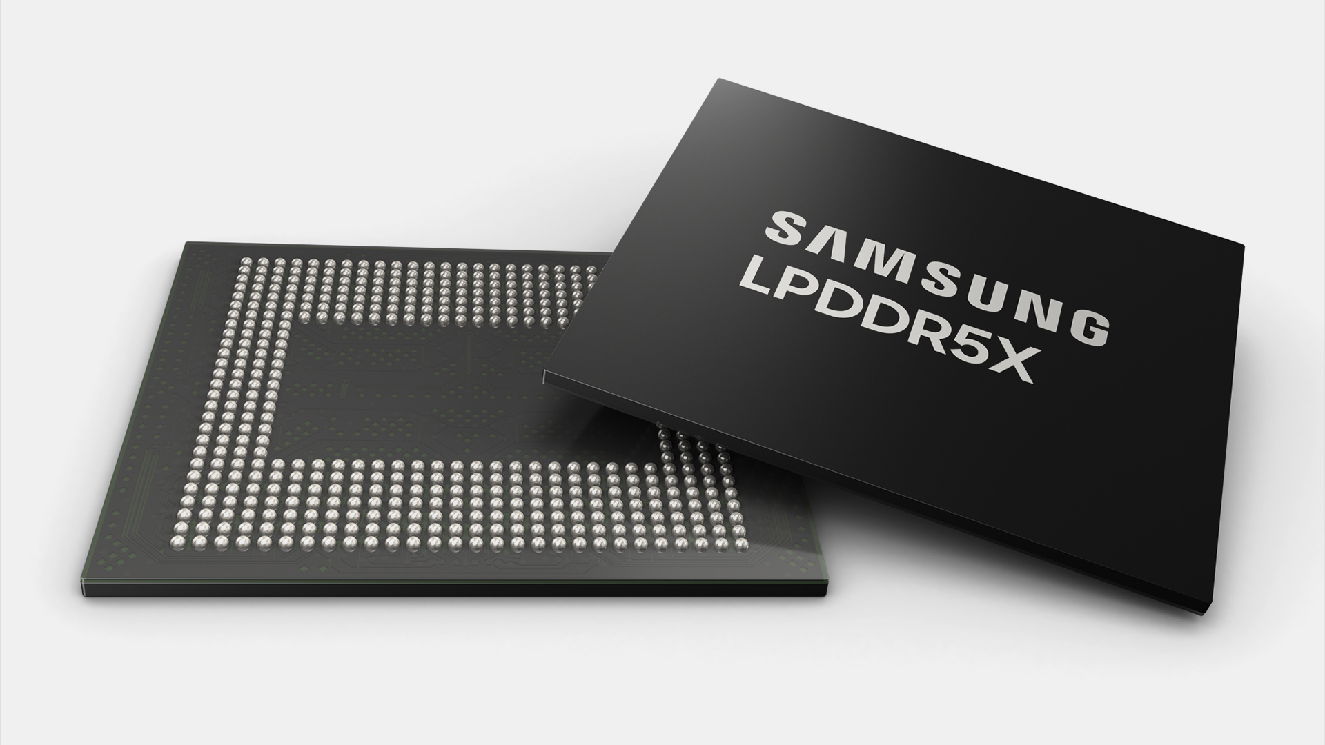
    Samsung has unveiled the world's thinnest LPDDR5X DRAM chip, which is just 0.65mm thin, or as thin as a fingernail. This chip is made for high-end smartphones, which typically have an onboard neural processing unit (NPU) for on-device AI processing. Samsung's newest LPDDR5X DRAM is just 0.65mm thin, making it the world's thinnest in its segment The newest LPDDR5X DRAM chip from Samsung is the world's thinnest 12nm-class chip. It is available in 12GB and 16GB capacities. This chip is made using
     

Samsung’s new smartphone memory chip is as thin as a fingernail

6. Srpen 2024 v 09:43

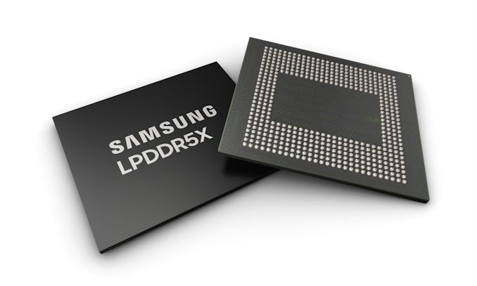
Samsung has unveiled the world's thinnest LPDDR5X DRAM chip, which is just 0.65mm thin, or as thin as a fingernail. This chip is made for high-end smartphones, which typically have an onboard neural processing unit (NPU) for on-device AI processing.

Samsung's newest LPDDR5X DRAM is just 0.65mm thin, making it the world's thinnest in its segment

Samsung LPDDR5X DRAM Chip

The newest LPDDR5X DRAM chip from Samsung is the world's thinnest 12nm-class chip. It is available in 12GB and 16GB capacities. This chip is made using four stacked layers, each containing two LPDDR DRAM chips. Due to its thin profile, it offers more space in mobile devices, allowing for a better thermal design. According to Samsung, its new memory chip improves heat resistance by up to 21.2% compared to the previous-generation LPDDR5X chip.

Samsung LPDDR5X DRAM Thinnest 0.65mm

Samsung optimized the printed circuit board (PCB), epoxy molding compound (EMC), and the back-lapping process to minimize the chip's height. The company plans to start supplying its new chip to smartphone manufacturers soon. It also announced that it will soon start making 24GB (6-layer) and 32GB (8-layer) LPDDR DRAM chips for future mobile devices.

YongCheol Bae, the Executive VP of Samsung's Memory Product Planning team, said, “Samsung’s LPDDR5X DRAM sets a new standard for high-performance on-device AI solutions, offering not only superior LPDDR performance but also advanced thermal management in an ultra-compact package. We are committed to continuous innovation through close collaboration with our customers, delivering solutions that meet the future needs of the low-power DRAM market.

Samsung LPDDR5X DRAM Thinnest Scale Samsung LPDDR5X DRAM Chip Connectors

Image Credits: Samsung

The post Samsung’s new smartphone memory chip is as thin as a fingernail appeared first on SamMobile.

  • ✇Semiconductor Engineering
  • Are You Ready For HBM4? A Silicon Lifecycle Management (SLM) PerspectiveFaisal Goriawalla
    Many factors are driving system-on-chip (SoC) developers to adopt multi-die technology, in which multiple dies are stacked in a three-dimensional (3D) configuration. Multi-die systems may make power and thermal issues more complex, and they have required major innovations in electronic design automation (EDA) implementation and test tools. These challenges are more than offset by the advantages of over traditional 2D designs, including: Reducing overall area Achieving much higher pin densities
     

Are You Ready For HBM4? A Silicon Lifecycle Management (SLM) Perspective

Many factors are driving system-on-chip (SoC) developers to adopt multi-die technology, in which multiple dies are stacked in a three-dimensional (3D) configuration. Multi-die systems may make power and thermal issues more complex, and they have required major innovations in electronic design automation (EDA) implementation and test tools. These challenges are more than offset by the advantages of over traditional 2D designs, including:

  • Reducing overall area
  • Achieving much higher pin densities
  • Reusing existing proven dies
  • Mixing heterogeneous die technologies
  • Quickly creating derivative designs for new applications

One of the most common uses of multi-die design is the interconnection of memory stacks and processors such as CPUs and GPUs. High Bandwidth Memory (HBM) is a standard interface specifically for 3D-stacked DRAM dies. It was defined by the JEDEC Solid State Technology Association in 2013, followed by HBM2 in 2016 and HBM3 in 2022. Many multi-die projects have used this standard for caches in advanced CPUs and other system-on-chip (SoC) designs used in high-end applications such as data centers, high-performance computing (HPC), and artificial intelligence (AI) processing.

Fig. 1: Example of a current HBM-based SoC.

JEDEC recently announced that it is nearing completion of HBM4 and published preliminary specifications. HBM4 has been developed to enhance data processing rates while maintaining higher bandwidth, lower power consumption, and increased capacity per die/stack. The initial agreement calls for speed bins up to 6.4 Gbps, although this will increase as memory vendors develop new chips and refine the technology. This speed will benefit applications that require efficient handling of large datasets and complex calculations.

HBM4 is introducing a doubled channel count per stack over HBM3. The new version of the standard features a 2048-bit memory interface, as compared to 1024 bits in previous versions, as shown in figure 1. This intent is to double the number of bits without increasing the footprint of HBM memory stacks, thus doubling the interconnection density as well.

Different memory configurations will require various interposers to accommodate the differing footprints. HBM4 will specify 24 Gb and 32 Gb layers, with options for supporting 4-high, 8-high, 12-high and 16-high TSV stacks. As an example configuration, a 16-high based on 32 Gb layers will offer a capacity of 64 GB, which means that a processor with four memory modules can support 256 GB of memory with a peak bandwidth of 6.56 TB/s using an 8,192-bit interface.

The move from HBM3 to HBM4 will require further evolution in multi-die support across a wide range of EDA tools. The 2048-bit memory interface requires a significant increase in the number of through-silicon vias (TSVs) routed through a memory stack. This will mean shrinking the external bump pitch as the total number of micro bumps increases significantly. In addition, support for 16-high TSV stacks brings new complexity in wiring up an even larger number of DRAM dies without defects.

Test challenges are likely to be a dominant part of the transition. Any signal integrity issues after assembly and multi-die packaging become more difficult to diagnose and debug since probing is not feasible. Further, some defects may marginally pass production/manufacturing test but subsequently fail in the field. Thus, test of the future HBM4-based subsystem needs to be accomplished not just at production test but also in-system to account for aging-related defects.

Being able to monitor real-time data during mission mode operation in the field is greatly preferable to having to take the system offline for unplanned service. This “predictive maintenance” allows the end user to be proactive rather than reactive. HBM provides capabilities for in-system repair, for example swapping out a bad lane. Even if a defect requires physical hardware repair, detecting it before system failure enables scheduled maintenance rather than unplanned downtime.

As shown in figure 1, HBM systems typically have a base die that includes an HBM controller, a basic/fixed test engine provided by the DRAM vendor, and Direct Access (DA) ports. The new industry trend is for the base die to be manufactured on a standard logic process rather than the DRAM process. The SoC designer should include in the base die a flexible built-in self-test (BIST) engine that allows different algorithms to be used to trade off high coverage versus test time depending on the scenario.

This engine must be programmable to handle different latencies, address ranges, and timing of test operations that vary across DRAM vendors. It may also need to support post-package repair (PPR) for HBM DRAM to delay any “truck roll-out” for in-field service. The diagnostics performed by the BIST engine must be precise, showing the failing bank, row address, column address, etc. if there is a defect detected in the DRAM stack. Figure 2 shows an example.

Fig. 2: Example fault diagnosis for HBM stack.

As an industry leader in multi-die EDA and IP solutions, Synopsys provides all the technology needed for HBM manufacturing yield optimization and in-field silicon health monitoring. Signal Integrity Monitors (SIMs) are embedded in physical layer (PHY) IP blocks for on-demand signal quality measurement for interconnects. This allows users to create 1D eye diagrams for interconnect signals during both production test and in-field operation. SIMs measure timing margins, enable HBM lane test/repair, and mitigate against silent data corruption (SDC), part of an effective silicon lifecycle management (SLM) solution.

Synopsys SMS ext-RAM is a programmable and synthesizable engine that performs test, repair, and diagnostics for memory systems, including HBM. SMS ext-RAM ensures high test coverage and supports power-on self-test (POST) with the flexibility to run custom memory algorithms in-field. As shown in figure 2, it detects a wide range of defects in memory dies, including stuck-at faults, read destructive faults, write destructive faults, deceptive read destructive faults, and row hammering.

A real world case study of a project using HBM with the Synopsys solutions is available. These solutions are scaling to support the emerging HBM4 standard, ensuring continued success.

The post Are You Ready For HBM4? A Silicon Lifecycle Management (SLM) Perspective appeared first on Semiconductor Engineering.

Secure Low-Cost In-DRAM Trackers For Mitigating Rowhammer (Georgia Tech, Google, Nvidia)

A new technical paper titled “MINT: Securely Mitigating Rowhammer with a Minimalist In-DRAM Tracker” was published by researchers at Georgia Tech, Google, and Nvidia.

Abstract
“This paper investigates secure low-cost in-DRAM trackers for mitigating Rowhammer (RH). In-DRAM solutions have the advantage that they can solve the RH problem within the DRAM chip, without relying on other parts of the system. However, in-DRAM mitigation suffers from two key challenges: First, the mitigations are synchronized with refresh, which means we cannot mitigate at arbitrary times. Second, the SRAM area available for aggressor tracking is severely limited, to only a few bytes. Existing low-cost in-DRAM trackers (such as TRR) have been broken by well-crafted access patterns, whereas prior counter-based schemes require impractical overheads of hundreds or thousands of entries per bank. The goal of our paper is to develop an ultra low-cost secure in-DRAM tracker.

Our solution is based on a simple observation: if only one row can be mitigated at refresh, then we should ideally need to track only one row. We propose a Minimalist In-DRAM Tracker (MINT), which provides secure mitigation with just a single entry. At each refresh, MINT probabilistically decides which activation in the upcoming interval will be selected for mitigation at the next refresh. MINT provides guaranteed protection against classic single and double-sided attacks. We also derive the minimum RH threshold (MinTRH) tolerated by MINT across all patterns. MINT has a MinTRH of 1482 which can be lowered to 356 with RFM. The MinTRH of MINT is lower than a prior counter-based design with 677 entries per bank, and is within 2x of the MinTRH of an idealized design that stores one-counter-per-row. We also analyze the impact of refresh postponement on the MinTRH of low-cost in-DRAM trackers, and propose an efficient solution to make such trackers compatible with refresh postponement.”

Find the technical paper here. Preprint published July 2024.

Qureshi, Moinuddin, Salman Qazi, and Aamer Jaleel. “MINT: Securely Mitigating Rowhammer with a Minimalist In-DRAM Tracker.” arXiv preprint arXiv:2407.16038 (2024).

The post Secure Low-Cost In-DRAM Trackers For Mitigating Rowhammer (Georgia Tech, Google, Nvidia) appeared first on Semiconductor Engineering.

  • ✇Semiconductor Engineering
  • LPDDR Memory Is Key For On-Device AI PerformanceNidish Kamath
    Low-Power Double Data Rate (LPDDR) emerged as a specialized high performance, low power memory for mobile phones. Since its first release in 2006, each new generation of LPDDR has delivered the bandwidth and capacity needed for major shifts in the mobile user experience. Once again, LPDDR is at the forefront of another key shift as the next wave of generative AI applications will be built into our mobile phones and laptops. AI on endpoints is all about efficient inference. The process of employi
     

LPDDR Memory Is Key For On-Device AI Performance

24. Červen 2024 v 09:02

Low-Power Double Data Rate (LPDDR) emerged as a specialized high performance, low power memory for mobile phones. Since its first release in 2006, each new generation of LPDDR has delivered the bandwidth and capacity needed for major shifts in the mobile user experience. Once again, LPDDR is at the forefront of another key shift as the next wave of generative AI applications will be built into our mobile phones and laptops.

AI on endpoints is all about efficient inference. The process of employing trained AI models to make predictions or decisions requires specialized memory technologies with greater performance that are tailored to the unique demands of endpoint devices. Memory for AI inference on endpoints requires getting the right balance between bandwidth, capacity, power and compactness of form factor.

LPDDR evolved from DDR memory technology as a power-efficient alternative; LPDDR5, and the optional extension LPDDR5X, are the most recent updates to the standard. LPDDR5X is focused on improving performance, power, and flexibility; it offers data rates up to 8.533 Gbps, significantly boosting speed and performance. Compared to DDR5 memory, LPDDR5/5X limits the data bus width to 32 bits, while increasing the data rate. The switch to a quarter-speed clock, as compared to a half-speed clock in LPDDR4, along with a new feature – Dynamic Voltage Frequency Scaling – keeps the higher data rate LPDDR5 operation within the same thermal budget as LPDDR4-based devices.

Given the space considerations of mobiles, combined with greater memory needs for advanced applications, LPDDR5X can support capacities of up to 64GB by using multiple DRAM dies in a multi-die package. Consider the example of a 7B LLaMa 2 model: the model consumes 3.5GB of memory capacity if based on INT4. A LPDDR5X package of x64, with two LPDDR5X devices per package, provides an aggregate bandwidth of 68 GB/s and, therefore, a LLaMa 2 model can run inference at 19 tokens per second.

As demand for more memory performance grows, we see LPDDR5 evolve in the market with the major vendors announcing additional extensions to LPDDR5 known as LPDDR5T, with the T standing for turbo. LPDDR5T boosts performance to 9.6 Gbps enabling an aggregate bandwidth of 76.8 GB/s in a x64 package of multiple LPDDR5T stacks. Therefore, the above example of a 7B LLaMa 2 model can run inference at 21 tokens per second.

With its low power consumption and high bandwidth capabilities, LPDDR5 is a great choice of memory not just for cutting-edge mobile devices, but also for AI inference on endpoints where power efficiency and compact form factor are crucial considerations. Rambus offers a new LPDDR5T/5X/5 Controller IP that is fully optimized for use in applications requiring high memory throughput and low latency. The Rambus LPDDR5T/5X/5 Controller enables cutting-edge LPDDR5T memory devices and supports all third-party LPDDR5 PHYs. It maximizes bus bandwidth and minimizes latency via look-ahead command processing, bank management and auto-precharge. The controller can be delivered with additional cores such as the In-line ECC or Memory Analyzer cores to improve in-field reliability, availability and serviceability (RAS).

The post LPDDR Memory Is Key For On-Device AI Performance appeared first on Semiconductor Engineering.

DRAM Microarchitectures And Their Impacts On Activate-Induced Bitflips Such As RowHammer 

19. Květen 2024 v 22:57

A technical paper titled “DRAMScope: Uncovering DRAM Microarchitecture and Characteristics by Issuing Memory Commands” was published by researchers at Seoul National University and University of Illinois at Urbana-Champaign.

Abstract:

“The demand for precise information on DRAM microarchitectures and error characteristics has surged, driven by the need to explore processing in memory, enhance reliability, and mitigate security vulnerability. Nonetheless, DRAM manufacturers have disclosed only a limited amount of information, making it difficult to find specific information on their DRAM microarchitectures. This paper addresses this gap by presenting more rigorous findings on the microarchitectures of commodity DRAM chips and their impacts on the characteristics of activate-induced bitflips (AIBs), such as RowHammer and RowPress. The previous studies have also attempted to understand the DRAM microarchitectures and associated behaviors, but we have found some of their results to be misled by inaccurate address mapping and internal data swizzling, or lack of a deeper understanding of the modern DRAM cell structure. For accurate and efficient reverse-engineering, we use three tools: AIBs, retention time test, and RowCopy, which can be cross-validated. With these three tools, we first take a macroscopic view of modern DRAM chips to uncover the size, structure, and operation of their subarrays, memory array tiles (MATs), and rows. Then, we analyze AIB characteristics based on the microscopic view of the DRAM microarchitecture, such as 6F^2 cell layout, through which we rectify misunderstandings regarding AIBs and discover a new data pattern that accelerates AIBs. Lastly, based on our findings at both macroscopic and microscopic levels, we identify previously unknown AIB vulnerabilities and propose a simple yet effective protection solution.”

Find the technical paper here. Published May 2024.

Nam, Hwayong, Seungmin Baek, Minbok Wi, Michael Jaemin Kim, Jaehyun Park, Chihun Song, Nam Sung Kim, and Jung Ho Ahn. “DRAMScope: Uncovering DRAM Microarchitecture and Characteristics by Issuing Memory Commands.” arXiv preprint arXiv:2405.02499 (2024).

Related Reading
Securing DRAM Against Evolving Rowhammer Threats
A multi-layered, system-level approach is crucial to DRAM protection.


The post DRAM Microarchitectures And Their Impacts On Activate-Induced Bitflips Such As RowHammer  appeared first on Semiconductor Engineering.

  • ✇Semiconductor Engineering
  • DDR5 PMICs Enable Smarter, Power-Efficient Memory ModulesTim Messegee
    Power management has received increasing focus in microelectronic systems as the need for greater power density, efficiency and precision have grown apace. One of the important ongoing trends in service of these needs has been the move to localizing power delivery. To optimize system power, it’s best to deliver as high a voltage as possible to the endpoint where the power is consumed. Then at the endpoint, that incoming high voltage can be regulated into the lower voltages with higher currents r
     

DDR5 PMICs Enable Smarter, Power-Efficient Memory Modules

16. Květen 2024 v 09:05

Power management has received increasing focus in microelectronic systems as the need for greater power density, efficiency and precision have grown apace. One of the important ongoing trends in service of these needs has been the move to localizing power delivery. To optimize system power, it’s best to deliver as high a voltage as possible to the endpoint where the power is consumed. Then at the endpoint, that incoming high voltage can be regulated into the lower voltages with higher currents required by the endpoint components.

We saw this same trend play out in the architecting of the DDR5 generation of computer main memory. In planning for DDR5, the industry laid out ambitious goals for memory bandwidth and capacity. Concurrently, the aim was to maintain power within the same envelope as DDR4 on a per module basis. In order to achieve these goals, DDR5 required a smarter DIMM architecture; one that would embed more intelligence in the DIMM and increase its power efficiency. One of the biggest architectural changes of this smarter DIMM architecture was moving power management from the motherboard to an on-module Power Management IC (PMIC) on each DDR5 RDIMM.

In previous DDR generations, the power regulator on the motherboard had to deliver a low voltage at high current across the motherboard, through a connector and then onto the DIMM. As supply voltages were reduced over time (to maintain power levels at higher data rates), it was a growing challenge to maintain the desired voltage level because of IR drop. By implementing a PMIC on the DDR5 RDIMM, the problem with IR drop was essentially eliminated.

In addition, the on-DIMM PMIC allows for very fine-grain control of the voltage levels supplied to the various components on the DIMM. As such, DIMM suppliers can really dial in the best power levels for the performance target of a particular DIMM configuration. On-DIMM PMICs also offered an economic benefit. Power management on the motherboard meant the regulator had to be designed to support a system with fully populated DIMMs. On-DIMM PMICs means only paying for the power management capacity you need to support your specific system memory configuration.

The upshot is that power management has become a major enabler of increasing memory performance. Advancing memory performance has been the mission of Rambus for nearly 35 years. We’re intimate with memory subsystem design on modules, with expertise across many critical enabling technologies, and have demonstrated the disciplines required to successfully develop chips for the challenging module environment with its increased power density, space constraints and complex thermal management challenges.

As part of the development of our DDR5 memory interface chipset, Rambus built a world-class power management team and has now introduced a new family of DDR5 server PMICs. This new server PMIC product family lays the foundation for a roadmap of future power management chips. As AI continues to expand from training to inference, increasing demands on memory performance will extend beyond servers to client systems and drive the need for new PMIC solutions tailored for emerging use cases and form factors across the computing landscape.

Resources:

The post DDR5 PMICs Enable Smarter, Power-Efficient Memory Modules appeared first on Semiconductor Engineering.

  • ✇Semiconductor Engineering
  • SRAM Security Concerns GrowKaren Heyman
    SRAM security concerns are intensifying as a combination of new and existing techniques allow hackers to tap into data for longer periods of time after a device is powered down. This is particularly alarming as the leading edge of design shifts from planar SoCs to heterogeneous systems in package, such as those used in AI or edge processing, where chiplets frequently have their own memory hierarchy. Until now, most cybersecurity concerns involving volatile memory have focused on DRAM, because it
     

SRAM Security Concerns Grow

9. Květen 2024 v 09:08

SRAM security concerns are intensifying as a combination of new and existing techniques allow hackers to tap into data for longer periods of time after a device is powered down.

This is particularly alarming as the leading edge of design shifts from planar SoCs to heterogeneous systems in package, such as those used in AI or edge processing, where chiplets frequently have their own memory hierarchy. Until now, most cybersecurity concerns involving volatile memory have focused on DRAM, because it is often external and easier to attack. SRAM, in contrast, does not contain a component as obviously vulnerable as a heat-sensitive capacitor, and in the past it has been harder to pinpoint. But as SoCs are disaggregated and more features are added into devices, SRAM is becoming a much bigger security concern.

The attack scheme is well understood. Known as cold boot, it was first identified in 2008, and is essentially a variant of a side-channel attack. In a cold boot approach, an attacker dumps data from internal SRAM to an external device, and then restarts the system from the external device with some code modification. “Cold boot is primarily targeted at SRAM, with the two primary defenses being isolation and in-memory encryption,” said Vijay Seshadri, distinguished engineer at Cycuity.

Compared with network-based attacks, such as DRAM’s rowhammer, cold boot is relatively simple. It relies on physical proximity and a can of compressed air.

The vulnerability was first described by Edward Felton, director of Princeton University’s Center for Information Technology Policy, J. Alex Halderman, currently director of the Center for Computer Security & Society at the University of Michigan, and colleagues. The breakthrough in their research was based on the growing realization in the engineering research community that data does not vanish from memory the moment a device is turned off, which until then was a common assumption. Instead, data in both DRAM and SRAM has a brief “remanence.”[1]

Using a cold boot approach, data can be retrieved, especially if an attacker sprays the chip with compressed air, cooling it enough to slow the degradation of the data. As the researchers described their approach, “We obtained surface temperatures of approximately −50°C with a simple cooling technique — discharging inverted cans of ‘canned air’ duster spray directly onto the chips. At these temperatures, we typically found that fewer than 1% of bits decayed even after 10 minutes without power.”

Unfortunately, despite nearly 20 years of security research since the publication of the Halderman paper, the authors’ warning still holds true. “Though we discuss several strategies for mitigating these risks, we know of no simple remedy that would eliminate them.”

However unrealistic, there is one simple and obvious remedy to cold boot — never leave a device unattended. But given human behavior, it’s safer to assume that every device is vulnerable, from smart watches to servers, as well as automotive chips used for increasingly autonomous driving.

While the original research exclusively examined DRAM, within the last six years cold boot has proven to be one of the most serious vulnerabilities for SRAM. In 2018, researchers at Germany’s Technische Universität Darmstadt published a paper describing a cold boot attack method that is highly resistant to memory erasure techniques, and which can be used to manipulate the cryptographic keys produced by the SRAM physical unclonable function (PUF).

As with so many security issues, it’s been a cat-and-mouse game between remedies and counter-attacks. And because cold boot takes advantage of slowing down memory degradation, in 2022 Yang-Kyu Choi and colleagues at the Korea Advanced Institute of Science and Technology (KAIST), described a way to undo the slowdown with an ultra-fast data sanitization method that worked within 5 ns, using back bias to control the device parameters of CMOS.

Fig. 1: Asymmetric forward back-biasing scheme for permanent erasing. (a) All the data are reset to 1. (b) All the data are reset to 0. Whether all the data where reset to 1 or 0 is determined by the asymmetric forward back-biasing scheme. Source: KAIST/Creative Commons [2]

Fig. 1: Asymmetric forward back-biasing scheme for permanent erasing. (a) All the data are reset to 1. (b) All the data are reset to 0. Whether all the data where reset to 1 or 0 is determined by the asymmetric forward back-biasing scheme. Source: KAIST/Creative Commons [2]

Their paper, as well as others, have inspired new approaches to combating cold boot attacks.

“To mitigate the risk of unauthorized access from unknown devices, main devices, or servers, check the authenticated code and unique identity of each accessing device,” said Jongsin Yun, memory technologist at Siemens EDA. “SRAM PUF is one of the ways to securely identify each device. SRAM is made of two inverters cross-coupled to each other. Although each inverter is designed to be the same device, normally one part of the inverter has a somewhat stronger NMOS than the other due to inherent random dopant fluctuation. During the initial power-on process, SRAM data will be either data 1 or 0, depending on which side has a stronger device. In other words, the initial data state of the SRAM array at the power on is decided by this unique random process variation and most of the bits maintain this property for life. One can use this unique pattern as a fingerprint of a device. The SRAM PUF data is reconstructed with other coded data to form a cryptographic key. SRAM PUF is a great way to anchor its secure data into hardware. Hackers may use a DFT circuit to access the memory. To avoid insecurely reading the SRAM information through DFT, the security-critical design makes DFT force delete the data as an initial process of TEST mode.”

However, there can be instances where data may be required to be kept in a non-volatile memory (NVM). “Data is considered insecure if the NVM is located outside of the device,” said Yun. “Therefore, secured data needs to be stored within the device with write protection. One-time programmable (OTP) memory or fuses are good storage options to prevent malicious attackers from tampering with the modified information. OTP memory and fuses are used to store cryptographic keys, authentication information, and other critical settings for operation within the device. It is useful for anti-rollback, which prevents hackers from exploiting old vulnerabilities that have been fixed in newer versions.”

Chiplet vulnerabilities
Chiplets also could present another vector for attack, due to their complexity and interconnections. “A chiplet has memory, so it’s going to be attacked,” said Cycuity’s Seshadri. “Chiplets, in general, are going to exacerbate the problem, rather than keeping it status quo, because you’re going to have one chiplet talking to another. Could an attack on one chiplet have a side effect on another? There need to be standards to address this. In fact, they’re coming into play already. A chiplet provider has to say, ‘Here’s what I’ve done for security. Here’s what needs to be done when interfacing with another chiplet.”

Yun notes there is a further physical vulnerability for those working with chiplets and SiPs. “When multiple chiplets are connected to form a SiP, we have to trust data coming from an external chip, which creates further complications. Verification of the chiplet’s authenticity becomes very important for SiPs, as there is a risk of malicious counterfeit chiplets being connected to the package for hacking purposes. Detection of such counterfeit chiplets is imperative.”

These precautions also apply when working with DRAM. In all situations, Seshardi said, thinking about security has to go beyond device-level protection. “The onus of protecting DRAM is not just on the DRAM designer or the memory designer,” he said. “It has to be secured by design principles when you are developing. In addition, you have to look at this holistically and do it at a system level. You must consider all the other things that communicate with DRAM or that are placed near DRAM. You must look at a holistic solution, all the way from software down to things like the memory controller and then finally, the DRAM itself.”

Encryption as a backup
Data itself always must be encrypted as second layer of protection against known and novel attacks, so an organization’s assets will still be protected even if someone breaks in via cold boot or another method.

“The first and primary method of preventing a cold boot attack is limiting physical access to the systems, or physically modifying the systems case or hardware preventing an attacker’s access,” said Jim Montgomery, market development director, semiconductor at TXOne Networks. “The most effective programmatic defense against an attack is to ensure encryption of memory using either a hardware- or software-based approach. Utilizing memory encryption will ensure that regardless of trying to dump the memory, or physically removing the memory, the encryption keys will remain secure.”

Montgomery also points out that TXOne is working with the Semiconductor Manufacturing Cybersecurity Consortium (SMCC) to develop common criteria based upon SEMI E187 and E188 standards to assist DM’s and OEM’s to implement secure procedures for systems security and integrity, including controlling the physical environment.

What kind and how much encryption will depend on use cases, said Jun Kawaguchi, global marketing executive for Winbond. “Encryption strength for a traffic signal controller is going to be different from encryption for nuclear plants or medical devices, critical applications where you need much higher levels,” he said. “There are different strengths and costs to it.”

Another problem, in the post-quantum era, is that encryption itself may be vulnerable. To defend against those possibilities, researchers are developing post-quantum encryption schemes. One way to stay a step ahead is homomorphic encryption [HE], which will find a role in data sharing, since computations can be performed on encrypted data without first having to decrypt it.

Homomorphic encryption could be in widespread use as soon as the next few years, according to Ronen Levy, senior manager for IBM’s Cloud Security & Privacy Technologies Department, and Omri Soceanu, AI Security Group manager at IBM.  However, there are still challenges to be overcome.

“There are three main inhibitors for widespread adoption of homomorphic encryption — performance, consumability, and standardization,” according to Levy. “The main inhibitor, by far, is performance. Homomorphic encryption comes with some latency and storage overheads. FHE hardware acceleration will be critical to solving these issues, as well as algorithmic and cryptographic solutions, but without the necessary expertise it can be quite challenging.”

An additional issue is that most consumers of HE technology, such as data scientists and application developers, do not possess deep cryptographic skills, HE solutions that are designed for cryptographers can be impractical. A few HE solutions require algorithmic and cryptographic expertise that inhibit adoption by those who lack these skills.

Finally, there is a lack of standardization. “Homomorphic encryption is in the process of being standardized,” said Soceanu. “But until it is fully standardized, large organizations may be hesitant to adopt a cryptographic solution that has not been approved by standardization bodies.”

Once these issues are resolved, they predicted widespread use as soon as the next few years. “Performance is already practical for a variety of use cases, and as hardware solutions for homomorphic encryption become a reality, more use cases would become practical,” said Levy. “Consumability is addressed by creating more solutions, making it easier and hopefully as frictionless as possible to move analytics to homomorphic encryption. Additionally, standardization efforts are already in progress.”

A new attack and an old problem
Unfortunately, security never will be as simple as making users more aware of their surroundings. Otherwise, cold boot could be completely eliminated as a threat. Instead, it’s essential to keep up with conference talks and the published literature, as graduate students keep probing SRAM for vulnerabilities, hopefully one step ahead of genuine attackers.

For example, SRAM-related cold boot attacks originally targeted discrete SRAM. The reason is that it’s far more complicated to attack on-chip SRAM, which is isolated from external probing and has minimal intrinsic capacitance. However, in 2022, Jubayer Mahmod, then a graduate student at Virginia Tech and his advisor, associate professor Matthew Hicks, demonstrated what they dubbed “Volt Boot,” a new method that could penetrate on-chip SRAM. According to their paper, “Volt Boot leverages asymmetrical power states (e.g., on vs. off) to force SRAM state retention across power cycles, eliminating the need for traditional cold boot attack enablers, such as low-temperature or intrinsic data retention time…Unlike other forms of SRAM data retention attacks, Volt Boot retrieves data with 100% accuracy — without any complex post-processing.”

Conclusion
While scientists and engineers continue to identify vulnerabilities and develop security solutions, decisions about how much security to include in a design is an economic one. Cost vs. risk is a complex formula that depends on the end application, the impact of a breach, and the likelihood that an attack will occur.

“It’s like insurance,” said Kawaguchi. “Security engineers and people like us who are trying to promote security solutions get frustrated because, similar to insurance pitches, people respond with skepticism. ‘Why would I need it? That problem has never happened before.’ Engineers have a hard time convincing their managers to spend that extra dollar on the costs because of this ‘it-never-happened-before’ attitude. In the end, there are compromises. Yet ultimately, it’s going to cost manufacturers a lot of money when suddenly there’s a deluge of demands to fix this situation right away.”

References

  1. S. Skorobogatov, “Low temperature data remanence in static RAM”, Technical report UCAM-CL-TR-536, University of Cambridge Computer Laboratory, June 2002.
  2. Han, SJ., Han, JK., Yun, GJ. et al. Ultra-fast data sanitization of SRAM by back-biasing to resist a cold boot attack. Sci Rep 12, 35 (2022). https://doi.org/10.1038/s41598-021-03994-2

The post SRAM Security Concerns Grow appeared first on Semiconductor Engineering.

  • ✇AnandTech
  • Samsung Unveils 10.7Gbps LPDDR5X Memory - The Fastest Yet
    Samsung today has announced that they have developed an even faster generation of LPDDR5X memory that is set to top out at LPDDR5X-10700 speeds. The updated memory is slated to offer 25% better performance and 30% greater capacity compared to existing mobile DRAM devices from the company. The new chips also appear to be tangibly faster than Micron's LPDDR5X memory and SK hynix's LPDDR5T chips. Samsung's forthcoming LPDDR5X devices feature a data transfer rate of 10.7 GT/s as well as maximum cap
     

Samsung Unveils 10.7Gbps LPDDR5X Memory - The Fastest Yet

17. Duben 2024 v 16:00

Samsung today has announced that they have developed an even faster generation of LPDDR5X memory that is set to top out at LPDDR5X-10700 speeds. The updated memory is slated to offer 25% better performance and 30% greater capacity compared to existing mobile DRAM devices from the company. The new chips also appear to be tangibly faster than Micron's LPDDR5X memory and SK hynix's LPDDR5T chips.

Samsung's forthcoming LPDDR5X devices feature a data transfer rate of 10.7 GT/s as well as maximum capacity per stack of 32 GB. This allows Samsung's clients to equip their latest smartphones or laptops with 32 GB of low-power memory using just one DRAM package, which greatly simplifies their designs. Samsung says that 32 GB of memory will be particularly beneficial for on-device AI applications.

Samsung is using its latest-generation 12nm-class DRAM process technology to make its LPDDR5X-10700 devices, which allows the company to achieve the smallest LPDDR device size in the industry, the memory maker said.

In terms of power efficiency, Samsung claims that they have integrated multiple new power-saving features into the new LPDDR5X devices. These include an optimized power variation system that adjusts energy consumption based on workload, and expanded intervals for low-power mode that extend the periods of energy saving. These innovations collectively enhance power efficiency by 25% compared to earlier versions, benefiting mobile platforms by extending battery life, the company said.

“As demand for low-power, high-performance memory increases, LPDDR DRAM is expected to expand its applications from mainly mobile to other areas that traditionally require higher performance and reliability such as PCs, accelerators, servers and automobiles,” said YongCheol Bae, Executive Vice President of Memory Product Planning of the Memory Business at Samsung Electronics. “Samsung will continue to innovate and deliver optimized products for the upcoming on-device AI era through close collaboration with customers.”

Samsung plans to initiate mass production of the 10.7 GT/s LPDDR5X DRAM in the second half of this year. This follows a series of compatibility tests with mobile application processors and device manufacturers to ensure seamless integration into future products.

  • ✇AnandTech
  • SK hynix to Build $3.87 Billion Memory Packaging Fab in the U.S. for HBM4 and Beyond
    SK hynix this week announced plans to build its advanced memory packaging facility in West Lafayette, Indiana. The move can be considered as a milestone both for the memory maker and the U.S., as this is the first advanced memory packaging facility in the country and the company's first significant manufacturing operation in America. The facility will be used to build next-generation types of high-bandwidth memory (HBM) stacks when it begins operations in 2028. Also, SK hynix agreed to work on R
     

SK hynix to Build $3.87 Billion Memory Packaging Fab in the U.S. for HBM4 and Beyond

5. Duben 2024 v 13:00

SK hynix this week announced plans to build its advanced memory packaging facility in West Lafayette, Indiana. The move can be considered as a milestone both for the memory maker and the U.S., as this is the first advanced memory packaging facility in the country and the company's first significant manufacturing operation in America. The facility will be used to build next-generation types of high-bandwidth memory (HBM) stacks when it begins operations in 2028. Also, SK hynix agreed to work on R&D projects with Purdue University.

"We are excited to become the first in the industry to build a state-of-the-art advanced packaging facility for AI products in the United States that will help strengthen supply-chain resilience and develop a local semiconductor ecosystem," said SK hynix CEO Kwak Noh-Jung.

One of The Most Advanced Chip Packaging Facility Ever

The facility will handle assembly of HBM known good stacked dies (KGSDs), which consist of multiple memory devices stacked on a base die. Furthermore, it will be used to develop next-generations of HBM and will therefore house a packaging R&D line. However, the plant will not make DRAM dies themselves, and will likely source them from SK hynix's fabs in South Korea.

The plant will require SK hynix to invest $3.87 billion, which will make it one of the most advanced semiconductor packaging facilities in the world. Meanwhile, SK hynix held the investment agreement ceremony with representatives from Indiana State, Purdue University, and the U.S. government, which indicates parties financially involved in the project, but this week's event did not disclose whether SK hynix will receive any money from the U.S. government under the CHIPS Act or other funding initiatives.

The cost of the facility significantly exceeds that of packaging facilities built by other major players in the industry, such as ASE Group, Intel, and TSMC, which highlights how significant of an investment this is for SK hnix. In fact, $3.87 billion higher than advanced packaging CapEx budgets of Intel, TSMC and Samsung in 2023, based on estimates from Yole Intelligence.

Given that the fab comes online in 2028, based on SK hynix's product roadmap we'd expect that it will be used at least in part to assemble HBM4 and HBM4E stacks. Notably, since HBM4 and HBM4E stacks are set to feature a 2048-bit interface, their packaging process will be considerably more complex than the existing 1024-bit HBM3/HBM3E packaging and will require usage of more advanced tools, which is why it is poised to be more expensive than some existing advanced packaging facilities. Due to the extremely complex 2048-bit interface, many chip designers who are going to use HBM4/HBM4E are expected to integrate it directly onto their processors using hybrid bonding and not use silicon interposers. Unfortunately, it is unclear whether the SK hynix facility will be able to offer such service.

HBM is mainly used for AI and HPC applications, so it is strategically important to have its production in the U.S. Meanwhile, actual memory dies will still need to be made elsewhere, at dedicated DRAM fabs.

Purdue University Collaboration

In addition to support set to be provided by state and local governmens, SK hynix chose to establish its new facility in West Lafayette, Indiana, to collaborate with Purdue University as well as with Purdue's Birck Nanotechnology Center on R&D projects, which includes advanced packaging and heterogeneous integration.

SK hynix intends to work in partnership with Purdue University and Ivy Tech Community College to create training programs and multidisciplinary degree courses aimed at nurturing a skilled workforce and establishing a consistent stream of emerging talent for its advanced memory packaging facility and R&D operations.

"SK hynix is the global pioneer and dominant market leader in memory chips for AI," Purdue University President Mung Chiang said. "This transformational investment reflects our state and university's tremendous strength in semiconductors, hardware AI, and hard tech corridor. It is also a monumental moment for completing the supply chain of digital economy in our country through chips advanced packaging. Located at Purdue Research Park, the largest facility of its kind at a U.S. university will grow and succeed through innovation."

  • ✇Semiconductor Engineering
  • Exploring Process Scenarios To Improve DRAM Device PerformanceYu De Chen
    In the world of advanced semiconductor fabrication, creating precise device profiles (edge shapes) is an important step in achieving targeted on-chip electrical performance. For example, saddle fin profiles in a DRAM memory device must be precisely fabricated during process development in order to avoid memory performance issues. Saddle fins were introduced in DRAM devices to increase channel length, prevent short channel effects, and increase data retention times. Critical process equipment set
     

Exploring Process Scenarios To Improve DRAM Device Performance

18. Duben 2024 v 09:04

In the world of advanced semiconductor fabrication, creating precise device profiles (edge shapes) is an important step in achieving targeted on-chip electrical performance. For example, saddle fin profiles in a DRAM memory device must be precisely fabricated during process development in order to avoid memory performance issues. Saddle fins were introduced in DRAM devices to increase channel length, prevent short channel effects, and increase data retention times. Critical process equipment settings like etch selectivity, or the gas ratio of the etch process, can significantly impact the shape of fabricated saddle fin profiles. These process and profile changes have significant impact on DRAM device performance. It can be challenging to explore all possible saddle fin profile combinations using traditional silicon testing, since wafer-based testing is time-consuming and expensive. To address this issue, virtual fabrication software (SEMulator3D) can be used to test different saddle fin profile shapes without the time and cost of wafer-based development. In this article, we will review an example of using virtual fabrication for DRAM saddle fin profile development. We will also assess DRAM device performance under different saddle fin profile conditions. This methodology can be used to guide process and integration teams in the development of process recipes and specifications for DRAM devices.

The challenge of exploring different profiles

Imagine that you are a DRAM process engineer, and have received nominal process conditions, device specifications and a target saddle fin profile for a new DRAM design. You would like to explore some different process options and saddle fin profiles to improve the performance of your DRAM device. What should you do? This is a common situation for integration and process engineers during the early R&D stages of DRAM process development.

Traditional methods of exploring saddle fin profiles are difficult and sometimes impractical. These methods involve the creation of a series of unique saddle fin profiles on silicon wafers. The process is time-consuming, expensive, and in many cases impractical, due to the large number of scenarios that must be tested.

One solution to these challenges is to use virtual fabrication. SEMulator3D allows us to create and analyze saddle fin profiles within a virtual environment and to subsequently extract and compare device characteristics of these different profiles. The strength of this approach is its ability to accurately simulate the real-world performance of these devices, but to do so faster and less-expensively than using wafer-based testing.

Methodology

Let’s dive into the methodology behind our approach:

Creating saddle fin profiles in a virtual environment

First, we input the design data and process flow (or process steps) for our device in SEMulator3D. The software can then generate a “virtual” 3D DRAM structure and provide a visualization of saddle fin profiles (figure 1). In figure 1(a), a full 3D DRAM structure including the entire simulation domain is displayed. To enable detailed device study, we have cropped a small portion of the simulation domain from this large 3D area. In figure 1(b), we have extracted a cross sectional view of the saddle fin structure, which can be modified by varying a set of multi-etch steps in the process model. The section of the saddle fin that we would like to modify is identified as the “AA” (active area). We can finely tune the etch taper angle, AA/fin CD, fin height, taper angle and additional nominal device parameters to modify the AA profile.

Figure 1: Process flow set up by SEMulator3D containing 3 figures marked A,B and C. Figure A contains a 3D simulated DRAM structure, with metals, nitrides, oxides and silicon structures shown in different colors. Figure B contains a cross section view of the saddle fin, with the bitline, active area, CC and wordline areas highlighted in the figure. Figure C highlights the key specifications of the saddle fin profile that can will be changed during simulation, including the etch taper angle, AA/fin CD, fin height, and taper angle to modify the saddle fin profile and shape.

Fig. 1: Process flow set up by SEMulator3D: (a) DRAM structure and (b) Cross section view of saddle fin along with key specifications of the saddle fin profile.

Using the structures that we have built in SEMulator3D, we can next assign dopants and ports to the simulated structure and perform electrical performance evaluation. Accurately assigning dopant species, and defining dopant concentrations within the structure, is critical to ensuring the accuracy of our simulation. In figure 2(a), we display a dopant concentration distribution generated in SEMulator3D.

Ports are contact points in the model which are used to apply or extract electrical signals during a device study. Proper assignment of the ports is very important. Figure 2(b) provides an example of port assignment in our test DRAM structure. By accurately assigning the ports and dopants, we can extract the device’s electrical characteristics under different process scenarios.

Figure 2: Dopant concentration and Port Setup for the DRAM device, marked at Figures 2A and 2B. In Figure 2(a), we display a dopant concentration distribution generated in SEMulator3D. The highest dopant concentration is found in the center of the device, shown in red and yellow. Figure 2(b) provides an example of port assignment in our test DRAM structure, with assignments shown against a device cross-section. Ports are assigned at the drain, source and gate of the device.

Fig. 2: (a) Dopant concentration and (b) Port assignments (in blue).

Manufacturability validation

It is important to ensure that our simulation models match real world results. We can validate our model against cross-sectional images (SEM or TEM images) from an actual fabricated device. To ensure that our simulated device matches the behavior of an actual manufactured chip, we can create real silicon test wafers containing DRAM structures with different saddle fin profiles. To study different saddle fin profiles, we will use different etch recipes on an etch machine to vary the DRAM wordline etch step. This allows us to create specific saddle fin profiles in silicon that can be compared to our simulated profiles. A process engineer can change etch recipes and easily create silicon-based etch profiles that match simulated cross section images, as shown in figure 3. In this case, the engineer created a nominal (Process of Record) profile, a “round” profile (with a rounded top), and a triangular shaped profile (with a triangular top). This wafer-based data is not only used to test electrical performance of the DRAM under different saddle fin profile conditions, but can also be fed back into the virtual model to calibrate the model and ensure that it is accurate during future use.

Figure 3: Cross section TEM/SEM images of saddle fin profiles taken from actual silicon devices are displayed, compared to the predicted model results from SEMulator3D. 3 side-by-side TEM images are shown for the saddle fin profiles vs. the model results, for : (a) Nominal condition (Process of Record), (b) Round profile and (c) Triangle profile

Fig. 3: Cross section images vs. models: (a) Nominal condition (Process of Record), (b) Round profile and (c) Triangle profile.

Device simulation and validation

In the final stage of our study, we will review the electrical simulation results for different saddle fin profile shapes. Figure 4 displays simulated electrical performance results for the round profile and triangular saddle fin profile. For each of the two profiles, the value of the transistor Subthreshold Swing (SS), On Current (Ion), and Threshold Voltage (Vt) are displayed, with the differences shown. Process integration engineers can use this type of simulation to compare device performance using different process approaches. The same electrical performance differences (trend) were seen on actual fabricated devices, validating the accuracy and reliability of our simulation approach.

Figure 4: Simulated electrical performance results for the round profile and triangular saddle fin profile. For each of the two profiles, the value of the transistor Subthreshold Swing (SS), On Current (Ion), and Threshold Voltage (Vt) are displayed, with the differences shown.

Fig. 4: Device electrical simulation results: the transistor performance difference between the Round and Triangular Saddle Fin profile is shown for Subthreshold Swing (SS), On Current (Ion) and Threshold Voltage (Vt).

Conclusions

SEMulator3D provides numerous benefits for the semiconductor manufacturing industry. It allows process integration teams to understand device performance under different process scenarios, and lets them easily explore new processes and architectural opportunities. In this article, we reviewed an example of how virtual fabrication can be used to assess DRAM device performance under different saddle fin profile conditions. Figure 5 displays a summary of the virtual fabrication process, and how we used it to understand, optimize and validate different process scenarios.

Figure 5: A summary of the virtual fabrication process undertaken in this study, including model setup, followed by an exploration of process conditions, followed by electrical analysis and final silicon verification. This process is circular, with the ability to repeat the loop as new information is collected.

Fig. 5: Summary of virtual fabrication process.

Virtual fabrication can be used to guide process and integration teams in the development of process recipes and specifications for any new memory or logic device, and to do so at greater speed and lower cost than silicon-based experimentation.

The post Exploring Process Scenarios To Improve DRAM Device Performance appeared first on Semiconductor Engineering.

  • ✇AnandTech
  • Samsung Unveils 10.7Gbps LPDDR5X Memory - The Fastest Yet
    Samsung today has announced that they have developed an even faster generation of LPDDR5X memory that is set to top out at LPDDR5X-10700 speeds. The updated memory is slated to offer 25% better performance and 30% greater capacity compared to existing mobile DRAM devices from the company. The new chips also appear to be tangibly faster than Micron's LPDDR5X memory and SK hynix's LPDDR5T chips. Samsung's forthcoming LPDDR5X devices feature a data transfer rate of 10.7 GT/s as well as maximum cap
     

Samsung Unveils 10.7Gbps LPDDR5X Memory - The Fastest Yet

17. Duben 2024 v 16:00

Samsung today has announced that they have developed an even faster generation of LPDDR5X memory that is set to top out at LPDDR5X-10700 speeds. The updated memory is slated to offer 25% better performance and 30% greater capacity compared to existing mobile DRAM devices from the company. The new chips also appear to be tangibly faster than Micron's LPDDR5X memory and SK hynix's LPDDR5T chips.

Samsung's forthcoming LPDDR5X devices feature a data transfer rate of 10.7 GT/s as well as maximum capacity per stack of 32 GB. This allows Samsung's clients to equip their latest smartphones or laptops with 32 GB of low-power memory using just one DRAM package, which greatly simplifies their designs. Samsung says that 32 GB of memory will be particularly beneficial for on-device AI applications.

Samsung is using its latest-generation 12nm-class DRAM process technology to make its LPDDR5X-10700 devices, which allows the company to achieve the smallest LPDDR device size in the industry, the memory maker said.

In terms of power efficiency, Samsung claims that they have integrated multiple new power-saving features into the new LPDDR5X devices. These include an optimized power variation system that adjusts energy consumption based on workload, and expanded intervals for low-power mode that extend the periods of energy saving. These innovations collectively enhance power efficiency by 25% compared to earlier versions, benefiting mobile platforms by extending battery life, the company said.

“As demand for low-power, high-performance memory increases, LPDDR DRAM is expected to expand its applications from mainly mobile to other areas that traditionally require higher performance and reliability such as PCs, accelerators, servers and automobiles,” said YongCheol Bae, Executive Vice President of Memory Product Planning of the Memory Business at Samsung Electronics. “Samsung will continue to innovate and deliver optimized products for the upcoming on-device AI era through close collaboration with customers.”

Samsung plans to initiate mass production of the 10.7 GT/s LPDDR5X DRAM in the second half of this year. This follows a series of compatibility tests with mobile application processors and device manufacturers to ensure seamless integration into future products.

  • ✇AnandTech
  • SK hynix to Build $3.87 Billion Memory Packaging Fab in the U.S. for HBM4 and Beyond
    SK hynix this week announced plans to build its advanced memory packaging facility in West Lafayette, Indiana. The move can be considered as a milestone both for the memory maker and the U.S., as this is the first advanced memory packaging facility in the country and the company's first significant manufacturing operation in America. The facility will be used to build next-generation types of high-bandwidth memory (HBM) stacks when it begins operations in 2028. Also, SK hynix agreed to work on R
     

SK hynix to Build $3.87 Billion Memory Packaging Fab in the U.S. for HBM4 and Beyond

5. Duben 2024 v 13:00

SK hynix this week announced plans to build its advanced memory packaging facility in West Lafayette, Indiana. The move can be considered as a milestone both for the memory maker and the U.S., as this is the first advanced memory packaging facility in the country and the company's first significant manufacturing operation in America. The facility will be used to build next-generation types of high-bandwidth memory (HBM) stacks when it begins operations in 2028. Also, SK hynix agreed to work on R&D projects with Purdue University.

"We are excited to become the first in the industry to build a state-of-the-art advanced packaging facility for AI products in the United States that will help strengthen supply-chain resilience and develop a local semiconductor ecosystem," said SK hynix CEO Kwak Noh-Jung.

One of The Most Advanced Chip Packaging Facility Ever

The facility will handle assembly of HBM known good stacked dies (KGSDs), which consist of multiple memory devices stacked on a base die. Furthermore, it will be used to develop next-generations of HBM and will therefore house a packaging R&D line. However, the plant will not make DRAM dies themselves, and will likely source them from SK hynix's fabs in South Korea.

The plant will require SK hynix to invest $3.87 billion, which will make it one of the most advanced semiconductor packaging facilities in the world. Meanwhile, SK hynix held the investment agreement ceremony with representatives from Indiana State, Purdue University, and the U.S. government, which indicates parties financially involved in the project, but this week's event did not disclose whether SK hynix will receive any money from the U.S. government under the CHIPS Act or other funding initiatives.

The cost of the facility significantly exceeds that of packaging facilities built by other major players in the industry, such as ASE Group, Intel, and TSMC, which highlights how significant of an investment this is for SK hnix. In fact, $3.87 billion higher than advanced packaging CapEx budgets of Intel, TSMC and Samsung in 2023, based on estimates from Yole Intelligence.

Given that the fab comes online in 2028, based on SK hynix's product roadmap we'd expect that it will be used at least in part to assemble HBM4 and HBM4E stacks. Notably, since HBM4 and HBM4E stacks are set to feature a 2048-bit interface, their packaging process will be considerably more complex than the existing 1024-bit HBM3/HBM3E packaging and will require usage of more advanced tools, which is why it is poised to be more expensive than some existing advanced packaging facilities. Due to the extremely complex 2048-bit interface, many chip designers who are going to use HBM4/HBM4E are expected to integrate it directly onto their processors using hybrid bonding and not use silicon interposers. Unfortunately, it is unclear whether the SK hynix facility will be able to offer such service.

HBM is mainly used for AI and HPC applications, so it is strategically important to have its production in the U.S. Meanwhile, actual memory dies will still need to be made elsewhere, at dedicated DRAM fabs.

Purdue University Collaboration

In addition to support set to be provided by state and local governmens, SK hynix chose to establish its new facility in West Lafayette, Indiana, to collaborate with Purdue University as well as with Purdue's Birck Nanotechnology Center on R&D projects, which includes advanced packaging and heterogeneous integration.

SK hynix intends to work in partnership with Purdue University and Ivy Tech Community College to create training programs and multidisciplinary degree courses aimed at nurturing a skilled workforce and establishing a consistent stream of emerging talent for its advanced memory packaging facility and R&D operations.

"SK hynix is the global pioneer and dominant market leader in memory chips for AI," Purdue University President Mung Chiang said. "This transformational investment reflects our state and university's tremendous strength in semiconductors, hardware AI, and hard tech corridor. It is also a monumental moment for completing the supply chain of digital economy in our country through chips advanced packaging. Located at Purdue Research Park, the largest facility of its kind at a U.S. university will grow and succeed through innovation."

  • ✇Semiconductor Engineering
  • Exploring Process Scenarios To Improve DRAM Device PerformanceYu De Chen
    In the world of advanced semiconductor fabrication, creating precise device profiles (edge shapes) is an important step in achieving targeted on-chip electrical performance. For example, saddle fin profiles in a DRAM memory device must be precisely fabricated during process development in order to avoid memory performance issues. Saddle fins were introduced in DRAM devices to increase channel length, prevent short channel effects, and increase data retention times. Critical process equipment set
     

Exploring Process Scenarios To Improve DRAM Device Performance

18. Duben 2024 v 09:04

In the world of advanced semiconductor fabrication, creating precise device profiles (edge shapes) is an important step in achieving targeted on-chip electrical performance. For example, saddle fin profiles in a DRAM memory device must be precisely fabricated during process development in order to avoid memory performance issues. Saddle fins were introduced in DRAM devices to increase channel length, prevent short channel effects, and increase data retention times. Critical process equipment settings like etch selectivity, or the gas ratio of the etch process, can significantly impact the shape of fabricated saddle fin profiles. These process and profile changes have significant impact on DRAM device performance. It can be challenging to explore all possible saddle fin profile combinations using traditional silicon testing, since wafer-based testing is time-consuming and expensive. To address this issue, virtual fabrication software (SEMulator3D) can be used to test different saddle fin profile shapes without the time and cost of wafer-based development. In this article, we will review an example of using virtual fabrication for DRAM saddle fin profile development. We will also assess DRAM device performance under different saddle fin profile conditions. This methodology can be used to guide process and integration teams in the development of process recipes and specifications for DRAM devices.

The challenge of exploring different profiles

Imagine that you are a DRAM process engineer, and have received nominal process conditions, device specifications and a target saddle fin profile for a new DRAM design. You would like to explore some different process options and saddle fin profiles to improve the performance of your DRAM device. What should you do? This is a common situation for integration and process engineers during the early R&D stages of DRAM process development.

Traditional methods of exploring saddle fin profiles are difficult and sometimes impractical. These methods involve the creation of a series of unique saddle fin profiles on silicon wafers. The process is time-consuming, expensive, and in many cases impractical, due to the large number of scenarios that must be tested.

One solution to these challenges is to use virtual fabrication. SEMulator3D allows us to create and analyze saddle fin profiles within a virtual environment and to subsequently extract and compare device characteristics of these different profiles. The strength of this approach is its ability to accurately simulate the real-world performance of these devices, but to do so faster and less-expensively than using wafer-based testing.

Methodology

Let’s dive into the methodology behind our approach:

Creating saddle fin profiles in a virtual environment

First, we input the design data and process flow (or process steps) for our device in SEMulator3D. The software can then generate a “virtual” 3D DRAM structure and provide a visualization of saddle fin profiles (figure 1). In figure 1(a), a full 3D DRAM structure including the entire simulation domain is displayed. To enable detailed device study, we have cropped a small portion of the simulation domain from this large 3D area. In figure 1(b), we have extracted a cross sectional view of the saddle fin structure, which can be modified by varying a set of multi-etch steps in the process model. The section of the saddle fin that we would like to modify is identified as the “AA” (active area). We can finely tune the etch taper angle, AA/fin CD, fin height, taper angle and additional nominal device parameters to modify the AA profile.

Figure 1: Process flow set up by SEMulator3D containing 3 figures marked A,B and C. Figure A contains a 3D simulated DRAM structure, with metals, nitrides, oxides and silicon structures shown in different colors. Figure B contains a cross section view of the saddle fin, with the bitline, active area, CC and wordline areas highlighted in the figure. Figure C highlights the key specifications of the saddle fin profile that can will be changed during simulation, including the etch taper angle, AA/fin CD, fin height, and taper angle to modify the saddle fin profile and shape.

Fig. 1: Process flow set up by SEMulator3D: (a) DRAM structure and (b) Cross section view of saddle fin along with key specifications of the saddle fin profile.

Using the structures that we have built in SEMulator3D, we can next assign dopants and ports to the simulated structure and perform electrical performance evaluation. Accurately assigning dopant species, and defining dopant concentrations within the structure, is critical to ensuring the accuracy of our simulation. In figure 2(a), we display a dopant concentration distribution generated in SEMulator3D.

Ports are contact points in the model which are used to apply or extract electrical signals during a device study. Proper assignment of the ports is very important. Figure 2(b) provides an example of port assignment in our test DRAM structure. By accurately assigning the ports and dopants, we can extract the device’s electrical characteristics under different process scenarios.

Figure 2: Dopant concentration and Port Setup for the DRAM device, marked at Figures 2A and 2B. In Figure 2(a), we display a dopant concentration distribution generated in SEMulator3D. The highest dopant concentration is found in the center of the device, shown in red and yellow. Figure 2(b) provides an example of port assignment in our test DRAM structure, with assignments shown against a device cross-section. Ports are assigned at the drain, source and gate of the device.

Fig. 2: (a) Dopant concentration and (b) Port assignments (in blue).

Manufacturability validation

It is important to ensure that our simulation models match real world results. We can validate our model against cross-sectional images (SEM or TEM images) from an actual fabricated device. To ensure that our simulated device matches the behavior of an actual manufactured chip, we can create real silicon test wafers containing DRAM structures with different saddle fin profiles. To study different saddle fin profiles, we will use different etch recipes on an etch machine to vary the DRAM wordline etch step. This allows us to create specific saddle fin profiles in silicon that can be compared to our simulated profiles. A process engineer can change etch recipes and easily create silicon-based etch profiles that match simulated cross section images, as shown in figure 3. In this case, the engineer created a nominal (Process of Record) profile, a “round” profile (with a rounded top), and a triangular shaped profile (with a triangular top). This wafer-based data is not only used to test electrical performance of the DRAM under different saddle fin profile conditions, but can also be fed back into the virtual model to calibrate the model and ensure that it is accurate during future use.

Figure 3: Cross section TEM/SEM images of saddle fin profiles taken from actual silicon devices are displayed, compared to the predicted model results from SEMulator3D. 3 side-by-side TEM images are shown for the saddle fin profiles vs. the model results, for : (a) Nominal condition (Process of Record), (b) Round profile and (c) Triangle profile

Fig. 3: Cross section images vs. models: (a) Nominal condition (Process of Record), (b) Round profile and (c) Triangle profile.

Device simulation and validation

In the final stage of our study, we will review the electrical simulation results for different saddle fin profile shapes. Figure 4 displays simulated electrical performance results for the round profile and triangular saddle fin profile. For each of the two profiles, the value of the transistor Subthreshold Swing (SS), On Current (Ion), and Threshold Voltage (Vt) are displayed, with the differences shown. Process integration engineers can use this type of simulation to compare device performance using different process approaches. The same electrical performance differences (trend) were seen on actual fabricated devices, validating the accuracy and reliability of our simulation approach.

Figure 4: Simulated electrical performance results for the round profile and triangular saddle fin profile. For each of the two profiles, the value of the transistor Subthreshold Swing (SS), On Current (Ion), and Threshold Voltage (Vt) are displayed, with the differences shown.

Fig. 4: Device electrical simulation results: the transistor performance difference between the Round and Triangular Saddle Fin profile is shown for Subthreshold Swing (SS), On Current (Ion) and Threshold Voltage (Vt).

Conclusions

SEMulator3D provides numerous benefits for the semiconductor manufacturing industry. It allows process integration teams to understand device performance under different process scenarios, and lets them easily explore new processes and architectural opportunities. In this article, we reviewed an example of how virtual fabrication can be used to assess DRAM device performance under different saddle fin profile conditions. Figure 5 displays a summary of the virtual fabrication process, and how we used it to understand, optimize and validate different process scenarios.

Figure 5: A summary of the virtual fabrication process undertaken in this study, including model setup, followed by an exploration of process conditions, followed by electrical analysis and final silicon verification. This process is circular, with the ability to repeat the loop as new information is collected.

Fig. 5: Summary of virtual fabrication process.

Virtual fabrication can be used to guide process and integration teams in the development of process recipes and specifications for any new memory or logic device, and to do so at greater speed and lower cost than silicon-based experimentation.

The post Exploring Process Scenarios To Improve DRAM Device Performance appeared first on Semiconductor Engineering.

  • ✇Semiconductor Engineering
  • Securing DRAM Against Evolving Rowhammer ThreatsAharon Etengoff
    Advanced process nodes and higher silicon densities are heightening DRAM’s susceptibility to Rowhammer attacks, as reduced cell spacing significantly decreases the hammer count needed for bit flips. Rowhammer exploits DRAM’s single-capacitor-per-bit design to trigger bit flips in adjacent cells through repeated memory row accesses. This vulnerability allows attackers to manipulate data, recover sensitive information, and crash processes or systems. First identified in 2014, evolving Rowhammer va
     

Securing DRAM Against Evolving Rowhammer Threats

7. Březen 2024 v 09:07

Advanced process nodes and higher silicon densities are heightening DRAM’s susceptibility to Rowhammer attacks, as reduced cell spacing significantly decreases the hammer count needed for bit flips.

Rowhammer exploits DRAM’s single-capacitor-per-bit design to trigger bit flips in adjacent cells through repeated memory row accesses. This vulnerability allows attackers to manipulate data, recover sensitive information, and crash processes or systems. First identified in 2014, evolving Rowhammer variants continue to target DRAM, successfully bypassing security techniques such as error correction code (ECC) and transactional row refresh (TRR).

Fig. 1: DRAMs on a DIMM, with corresponding mapping of row addresses and DRAM banks. A RowHammer attack can flip bits in the same victim row in multiple DRAMs, overwhelming ECC protection. Source: Rambus

Fig. 1: DRAMs on a DIMM, with corresponding mapping of row addresses and DRAM banks. A RowHammer attack can flip bits in the same victim row in multiple DRAMs, overwhelming ECC protection. Source: Rambus

Effectively protecting DRAM against Rowhammer requires a multi-layer, system-level implementation of robust security techniques, from encryption and obfuscation to enforced data isolation and advanced error correction schemes. This is easier said than done, however, as countermeasures can potentially impact power, performance, and area (PPA). Engineers should therefore evaluate PPA-security tradeoffs alongside key features and components at the start of the design process.

A top-down, system-level approach to securing DRAM
“Security is always a cat-and-mouse game, and the evolution of Rowhammer attacks and defenses is no different,” said Nicole Fern, senior security analyst at Riscure. “Researchers have demonstrated successful Rowhammer attacks on commercial DRAM modules employing both TRR and ECC, recovering TLS signing keys in several cryptographic libraries (Amazon-s2n (CVE-2022-42962), WolfSSL (CVE-2022-42961), and LibreSSL (CVE-2022-42963). Many speculate that real-world attacks are imminent. For countermeasures, the question should not be, ‘Will they ultimately be able to counter Rowhammer attacks in general?’ Rather, the question should be: ‘For a specific system and threat model, is the attack effort greater than the value of the assets being targeted and costs of a successful attack?’”

Traditionally, only PPA tradeoffs are considered during the silicon design process. However, recent hardware-based attacks, including Rowhammer, Meltdown, and Spectre, and those exploiting DVFS features to inject faults from software—such as clkscrew and Plundervolt—highlight the importance of prioritizing security during the design process. “Often, it is new features added for performance that create a foothold for attacks,” explained Fern. “As DRAM technology [nodes] shrink over time, with density and performance improving, susceptibility to Rowhammer increases. [Engineers] need to be aware of this effect and proactively design in appropriate countermeasures — with thorough testing ensuring these perform as expected as DRAM technology evolves.”

Jason Oberg, co-founder and CTO at Cycuity, agrees. “Hardware susceptibility is a key component of a larger chain of weaknesses used to exploit vulnerabilities. Rowhammer, a physical attack that’s done remotely, is one of those easy-to-exploit vectors, because if you can flip or modify a bit, you can chain that together with other software-based exploits. In isolation, it may be less of an issue, but in the context of a bigger strain of weaknesses that someone is exploiting, it’s problematic. Many systems vulnerable to Meltdown and Spectre, for example, are also points of concern for exploits like Rowhamer. You wouldn’t worry about these attacks on your smart light bulb or robot vacuum, but I would be concerned about my phone or laptop.”

To address these concerns, various encryption and obfuscation techniques have been proposed to protect DRAM from Rowhammer attacks. “If you encrypt or obfuscate your data, and then someone hammers a row and causes bits to flip, they won’t be able to target a specific bit,” Oberg explained. “They won’t know what the specific bit is. Whereas if it’s just plain text and it’s like a supervisor bit and they know where that supervisor bit is, then they can be very direct with what they’re doing.”

Although these techniques are crucial, Oberg emphasized that security considerations must be part of the design process, starting at the architectural level. “If I’m building a chip using licensed IP, I need to take a step back, analyze its function, and determine the assets that need to be protected,” Oberg noted. “From there, you can license a hardware-based root of trust. Maybe you trust one and not the other, even though it’s cheaper. These are the kind of decisions you should drive at the top level, and then try to manage as best you can without having full control of everything in your supply chain.”

Analyzing a system holistically also allows the design team to reduce the impact of security mitigation on PPA. “If you jump straight into saying, ‘I am concerned about memory,’ then you’re already very isolated,” he said. “If you start picking at each of the weaknesses independently, then the overhead goes up a lot higher because there may be an overlap between [mitigation techniques]. So you should take a higher-level view. It’s important to look at that top level and then drive your security program from that level. If you drive it from the bottom up, you’re going to have huge overheads, a lot of complexity, and you’re going to have problems.”

Ultimately, Oberg sees a combination of system-wide hardware and software solutions, paired with strict access controls and enforced data isolation, as a more effective method of countering exploits like Rowhammer. “In any multi-tenant or shared environment, containers are needed to isolate data. Data should also be assigned, for example, to processor thread A where it can’t be read by another thread. Of course, it can’t just be software. Foundation-level hardware protections are required. Otherwise, software protection will be subverted.”

Siloing processes and tagging memory
Kos Gitchev, senior technical market manager at Cadence, pointed to Arm’s confidential compute architecture (CCA) and memory tagging extension (MTE) as examples of a multi-layered, system-centric defense strategy against various attacks and exploits, including Rowhammer and RAMBleed. CCA ensures data protection during processing by isolating or siloing computation in a secure, hardware-backed environment, while MTE tags memory allocations with metadata that is verified during runtime operations. Although not specifically designed to counter Rowhammer or RAMBleed, both mechanisms help protect against such exploits.

“A Rowhammer attacker can’t say: ‘Well, I’ve taken over the machine and I want to go read this memory,’” Gitchev explained. “If you don’t have the appropriate MTE tags for your process, then you won’t be able to read it. The system will basically block it.”

To protect data held in DRAM, 128-bit or 256-bit AES encryption is also essential. “This is generally done by the memory subsystem, not the DRAM itself,” Gitchev noted. “Blocks of data will come in, they’ll get encrypted, and then pass to the memory. If anything happens to the encrypted data, it won’t properly decrypt. Encryption is almost always done in conjunction with ECC, so there are almost two layers of protection when you implement this scheme.”

Gitchev emphasized that encryption is only effective if keys are properly managed and secured. “A memory subsystem does the encryption. It has the algorithm and adds the XTS extension. Even when you write two blocks of the same data, they’ll look different on the bus to the memory. Of course, all of this can be overcome if someone compromises the encryption key.”

AES encryption can be added without major PPA penalties, making it an optimal choice for memory subsystems. “There are many different encryption schemes out there, but AES is easiest to implement,” said Gitchev. “Adding encryption, however, does increase the number of gates and power. To be fair, most of the memory subsystem power goes into driving the interface [for transferring data off-chip to the memory and back]. There is also a little bit of performance and area cost. The memory subsystem is now bigger because it needs to execute complex mathematical calculations for encryption and decryption in real time without significant latency.”

Tightly coupling encryption and decryption ciphering functions inside the DDR or LPDDR controllers facilitates maximum memory efficiency and lowest overall latency. “When doing both functions separately, certain functionality may have to be repeated, such as bus interface logic or support for read-modify-write operations,” said Ruud Derwig, system architect, solutions group at Synopsys. “When tightly integrated, the scheduler inside the controller can request encryption and decryption at the most optimal times, for example, when overlapping other controller operations or while waiting for data.”

Rowhammer and its variants aren’t necessarily the primary drivers for memory encryption solutions that require secure key management. “Inline memory encryption (IME) is mainly intended to defend against cold-boot attacks and provide confidential compute features,” Derwig said. “For example, a newly created virtual machine (VM) or process may get access to physical memory pages used previously by another VM or process when memory is not erased first, compromising the confidentiality of that previous computing context. With proper key management, IME mitigates these compromises. Or, when the hypervisor itself cannot be trusted, confidentiality of user data is still guaranteed by using different IME keys for different privilege levels and VMs.”

Nevertheless, IME contributes to Rowhammer attack countermeasures, as post-encryption data in the memory appears random to attackers. “Certain data patterns — rowstriped or checker patterns, for example — give the highest success rate for row hammering,” Derwig elaborated. “Moreover, when a single or a few bits are flipped, this is amplified to a full 128-bit decrypted block getting random data, so exploiting bit flips becomes much harder. When there is no attacker control over the changes, it is more likely to get detected by causing malfunctioning. IME [also offers] cryptographically strong integrity protection that mitigates bypassing less strong ECC protection.”

The cycle of Rowhammer attacks and countermeasures will continue as new vulnerabilities are identified and addressed. “Multi-level defenses and mitigations, such as hardware design of memory chips and memory controllers, as well as system software mitigations in hypervisors and operating systems, are needed to [counter] evolving threats,” Derwig added.

Bolstering DRAM reliability in data centers
Although Rowhammer can target any device equipped with DRAM, protecting the data center remains a priority for the semiconductor industry and many security researchers. “New memory used to debut in high-performance PCs and then move into servers,” said Steven Woo, fellow and distinguished inventor at Rambus Labs. “These days, new memory technologies debut for AI [applications] in data centers. The concern is, ‘What if somebody gains access to many servers in the data center and launches programs that intentionally try to repeatedly activate addresses?’ If enough bits flip and can’t be corrected, it could cause what looks like a large hardware fault. You might have to take down memory channels or a machine.”

While the risks of Rowhammer and other exploits in the data center are well known, the semiconductor industry may need more time to comprehensively bolster DRAM security and reliability at the design and system levels. “If you go back 25 or 30 years, nobody was really that concerned about power,” Woo stated. “You can dissipate the heat. You just burn a little more power to get more performance. But today, power is a first-class design parameter that everybody thinks about. Reliability is in that same place that power was in the 2000 to 2005 timeframe, where people are starting to realize, ‘Well, wait a minute, things aren’t infinitely reliable. We’re now going to have to consider DRAM reliability as a first-class design parameter.'”

As DRAM process geometries continue to shrink, electronic engineers will need to develop new or improved architectures and techniques that resist deliberate and repeated errors caused by attackers. “And the tradeoff is, ‘What are you willing to pay to do that? Is there a performance hit? Is there an area hit? Are we storing lots of extra bits?’ In 10 years, we’ll look back and we’ll be talking about reliability in the same way that we talk about power today,” he said.

Bolstering DRAM security and reliability without significantly impacting PPA was the primary driver behind the development of Rambus Labs’ RAMPART: Rowhammer mitigation and repair for server memory systems. Essentially, RAMPART mitigates Rowhammer attacks and improves server memory system reliability by remapping addresses in each DRAM, confining bit flips to a single device for any victim row address. When paired with existing error detection and correction methods, such as single-device data correction (SDDC) and patrol scrub, the system successfully detects and corrects bit flips. To effectively minimize mitigation overhead, RAMPART employs BRC-VL, a variation of DDR5’s bounded refresh configuration (BRC).

Fig. 2: RAMPART row address mappings produce unique neighbors, so Rowhammer attacks have different victim addresses in each DRAM. (a) Circular left shifts of controller row addresses based on unique DRAM IDs are shown. The tables at the bottom illustrate how controller row addresses map to internal bank rows in each DRAM. Row addresses 0x0000 and 0x0001 are bolded to highlight increasing separation with larger shifts. (b) Hammering controller row address 0x0001 flips bits in controller row addresses 0x0000 and 0x0002 in DRAM 0, but controller row addresses 0x8000 and 0x8001 in DRAM 1. A subsequent read to controller row address 0x0000 sees errors only from DRAM 0 that can be corrected with SDDC ECC. Source: Rambus

Fig. 2: RAMPART row address mappings produce unique neighbors, so Rowhammer attacks have different victim addresses in each DRAM. (a) Circular left shifts of controller row addresses based on unique DRAM IDs are shown. The tables at the bottom illustrate how controller row addresses map to internal bank rows in each DRAM. Row addresses 0x0000 and 0x0001 are bolded to highlight increasing separation with larger shifts. (b) Hammering controller row address 0x0001 flips bits in controller row addresses 0x0000 and 0x0002 in DRAM 0, but controller row addresses 0x8000 and 0x8001 in DRAM 1. A subsequent read to controller row address 0x0000 sees errors only from DRAM 0 that can be corrected with SDDC ECC. Source: Rambus

Assuming 70% area utilization and conservative routing, RAMPART reaches a speed of 2.85GHz in an area of 3910µm², or roughly 51K NAND2 gates. For a server with 1,024 banks, the total area required is only 0.1251mm². “We did a sample implementation at TSMC’s 7nm process, showing RAMPART’s small [footprint],” Woo said. “The controller side of it that does the tracking and figures out how often to issue a mitigation operation is very small, just a few gates. It’s very reasonable to implement something like this in a memory controller, and it has no die size impact as far as we can tell. There’s no latency impact on the accesses. It’s a very simple remapping change. And the DRAM is already doing remapping, so it’s not like asking for a new function. It’s simply modifying an existing function.

Conclusion
The continued proliferation of new and improved Rowhammer variants highlights the critical importance of implementing multi-layered, system-level countermeasures to protect DRAM, alongside of other key components and features. These should encompass a wide range of security techniques, from encryption and obfuscation to advanced error correction, address remapping, and data isolation. Still, to fully optimize performance and minimize latency, PPA security tradeoffs must be assessed from the top down at the start of the design process.

Related Reading
Power/Performance Costs Of Securing Systems
Security requires significant overhead, but it is no longer an option to ignore it. Cybercriminals will continue to exploit weak components.
Developing An Unbreakable Cybersecurity System
New approaches are in research, but threats continue to grow.
DRAM Choices Are Suddenly Much More Complicated
The number of options and tradeoffs is exploding as multiple flavors of DRAM are combined in a single design.

The post Securing DRAM Against Evolving Rowhammer Threats appeared first on Semiconductor Engineering.

❌
❌