Today the full screen experience (FSE) is generally available on Windows 11 handhelds currently in market, bringing performance optimizations and the ability to boot directly into Xbox for a smoother, more seamless way to play. Designed to minimize friction and get players into their games faster, this update helps deliver a console-like experience on handheld devices. For more information on how to set up, check out the full screen experience support page.
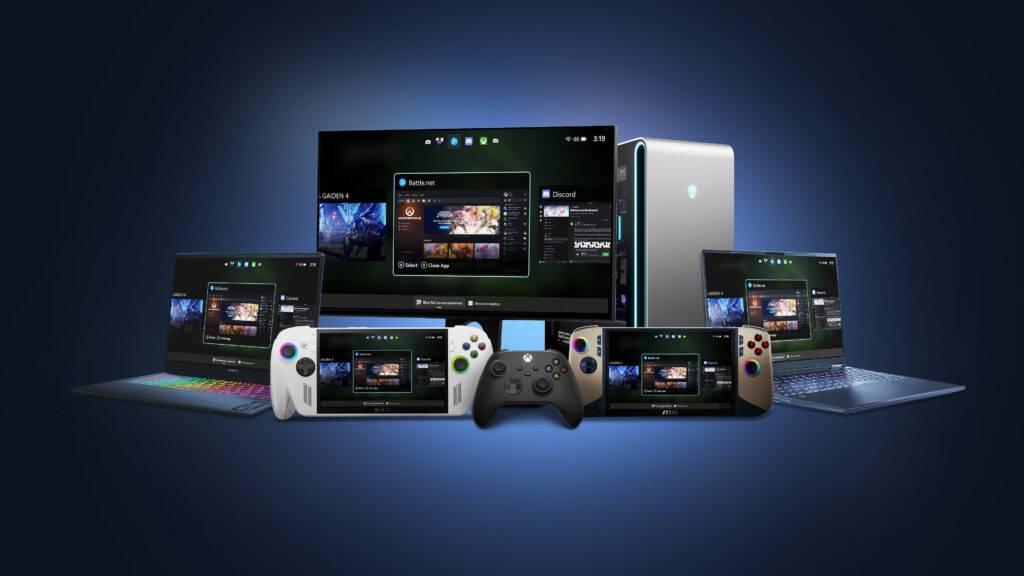
In addition to handhelds, the Xbox full screen experience is now available in preview for more Windows 11 PC form factors, such as laptops, desktops, and tablets, tailored for the PC experience.
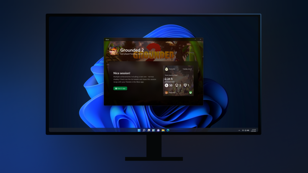
The Xbox full screen experience introduces a controller-navigable UI that brings an immersive, console-like experience to Windows 11 PC form factors. Designed for controller-first navigation, it provides a gaming-first, full-screen environment where players can easily browse and launch titles from across their game libraries- including most popular PC storefronts. A powerful Task Switcher enables quick movement between games and apps, delivering a seamless experience.
How to Get Access to the PC Preview: Join Xbox Insider and Windows Insider Program
- Join the Xbox Insider Program if you haven’t already: Xbox Insider Home | Xbox Support
- Install/Launch the Xbox Insider Hub app
- Navigate to Previews > PC Gaming Preview
- Join the Windows Insider Program Join the Windows Insider Program and manage Insider settings – Microsoft Support
- Join Beta or Dev channels
Once you’ve joined – how to enter FSE:
For more information about the Xbox full screen experience, including details about how to be among the first to try it out, visit Extending Xbox full screen experience to Windows 11 PC form factors.
How to Provide Feedback
Share your thoughts in Feedback Hub, accessible via keyboard shortcut (WIN + F) or via the Xbox PC App (by selecting “Report a Problem”). Be sure to submit your Feedback under Gaming and Xbox > Gaming Full Screen Experience.
How to Get Xbox Insider Support and Share Your Feedback
We want to thank all the Xbox Insiders for the feedback you share with us. If you’re an Xbox Insider looking for support, please join our community on the Xbox Insider subreddit, where official Xbox staff, moderators, and fellow Xbox Insiders are there to help. We recommend adding to threads with the same topic before posting a brand new one. This helps us support you the best we can! We’re grateful to our Insider community for the helpful feedback you provide, it continues to shape the future of Xbox.
For more information on the Xbox Insider Program, follow us on Twitter at @XboxInsider and keep an eye on this blog for all the latest news.
Other resources:
For more information: follow us on X/Twitter at @XboxInsider and this blog for announcements and more. And feel free to interact with the community on the Xbox Insider SubReddit.