FreshRSS

Normální zobrazení

Jsou dostupné nové články, klikněte pro obnovení stránky.
PředevčíremHlavní kanál
  • ✇Semiconductor Engineering
  • 3.5D: The Great CompromiseEd Sperling
    The semiconductor industry is converging on 3.5D as the next best option in advanced packaging, a hybrid approach that includes stacking logic chiplets and bonding them separately to a substrate shared by other components. This assembly model satisfies the need for big increases in performance while sidestepping some of the thorniest issues in heterogeneous integration. It establishes a middle ground between 2.5D, which already is in widespread use inside of data centers, and full 3D-ICs, which
     

3.5D: The Great Compromise

21. Srpen 2024 v 09:01

The semiconductor industry is converging on 3.5D as the next best option in advanced packaging, a hybrid approach that includes stacking logic chiplets and bonding them separately to a substrate shared by other components.

This assembly model satisfies the need for big increases in performance while sidestepping some of the thorniest issues in heterogeneous integration. It establishes a middle ground between 2.5D, which already is in widespread use inside of data centers, and full 3D-ICs, which the chip industry has been struggling to commercialize for the better part of a decade.

A 3.5D architecture offers several key advantages:

  • It creates enough physical separation to effectively address thermal dissipation and noise.
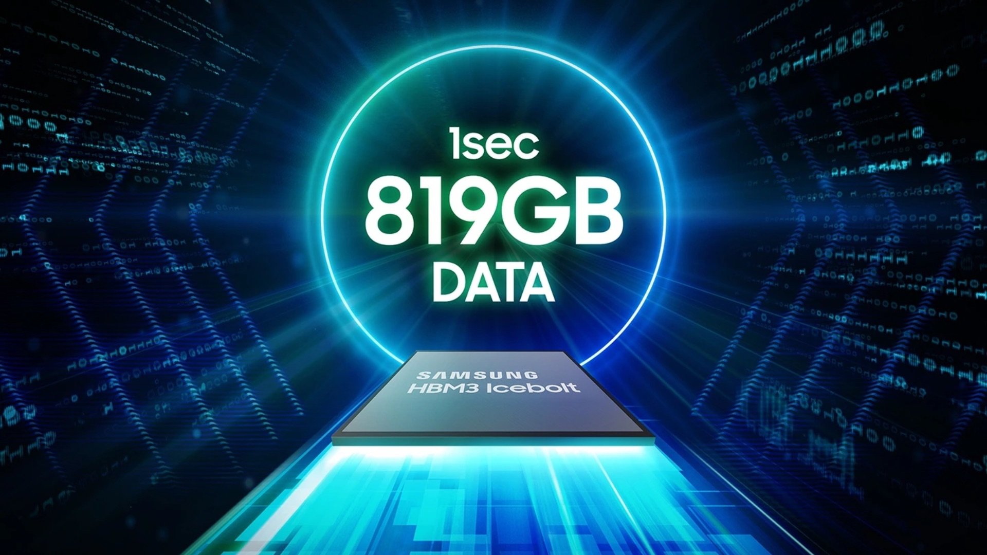
  • It provides a way to add more SRAM into high-speed designs. SRAM has been the go-to choice for processor cache since the mid-1960s, and remains an essential element for faster processing. But SRAM no longer scales at the same rate as digital transistors, so it is consuming more real estate (in percentage terms) at each new node. And because the size of a reticle is fixed, the best available option is to add area by stacking chiplets vertically.
  • By thinning the interface between processing elements and memory, a 3.5D approach also can shorten the distances that signals need to travel and greatly improve processing speeds well beyond a planar implementation. This is essential with large language models and AI/ML, where the amount of data that needs to be processed quickly is exploding.

Chipmakers still point to fully integrated 3D-ICs as the best performing alternative to a planar SoC, but packing everything into a 3D configuration makes it harder to deal with physical effects. Thermal dissipation is probably the most difficult to contend with. Workloads can vary significantly, creating dynamic thermal gradients and trapping heat in unexpected places, which in turn reduce the lifespan and reliability of chips. On top of that, power and substrate noise become more problematic at each new node, as do concerns about electromagnetic interference.

“What the market has adopted first is high-performance chips, and those produce a lot of heat,” said Marc Swinnen, director of product marketing at Ansys. “They have gone for expensive cooling systems with a huge number of fans and heat sinks, and they have opted for silicon interposers, which arguably are some of the most expensive technologies for connecting chips together. But it also gives the highest performance and is very good for thermal because it matches the coefficient of thermal expansion. Thermal is one of the big reasons that’s been successful. In addition to that, you may want bigger systems with more stuff that you can’t fit on one chip. That’s just a reticle-size limitation. Another is heterogeneous integration, where you want multiple different processes, like an RF process or the I/O, which don’t need to be in 5nm.”

A 3.5D assembly also provides more flexibility to add additional processor cores, and higher yield because known good die can be manufactured and tested separately, a concept first pioneered by Xilinx in 2011 at 28nm.

3.5D is a loose amalgamation of all these approaches. It can include two to three chiplets stacked on top of each other, or even multiple stacks laid out horizontally.

“It’s limited vertical, and not just for thermal reasons,” said Bill Chen, fellow and senior technical advisor at ASE Group. “It’s also for performance reasons. But thermal is the limiting factor, and we’ve talked about many different materials to help with that — diamond and graphene — but that limitation is still there.”

This is why the most likely combination, at least initially, will be processors stacked on SRAM, which simplifies the cooling. The heat generated by high utilization of different processing elements can be removed with heat sinks or liquid cooling. And with one or more thinned out substrates, signals will travel shorter distances, which in turn uses less power to move data back and forth between processors and memory.

“Most likely, this is going to be logic over memory on a logic process,” said Javier DeLaCruz, fellow and senior director of Silicon Ops Engineering at Arm. “These are all contained within an SoC normally, but a portion of that is going to be SRAM, which does not scale very well from node to node. So having logic over memory and a logic process is really the winning solution, and that’s one of the better use cases for 3D because that’s what really shortens your connectivity. A processor generally doesn’t talk to another processor. They talk to each other through memory, so having the memory on a different floor with no latency between them is pretty attractive.”

The SRAM doesn’t necessarily have to be at the same node as the processors advanced node, which also helps with yield, and reliability. At a recent Samsung Foundry event, Taejoong Song, the company’s vice president of foundry business development, showed a roadmap of a 3.5D configuration using a 2nm chiplet stacked on a 4nm chiplet next year, and a 1.4nm chiplet on top of a 2nm chiplet in 2027.


Fig. 1: Samsung’s heterogeneous integration roadmap showing stacked DRAM (HBM), chiplets and co-packaged optics. Source: Samsung Foundry

Intel Foundry’s approach is similar in many ways. “Our 3.5D technology is implemented on a substrate with silicon bridges,” said Kevin O’Buckley, senior vice president and general manager of Foundry Services at Intel. “This is not an incredibly costly, low-yielding, multi-reticle form-factor silicon, or even RDL. We’re using thin silicon slices in a much more cost-efficient fashion to enable that die-to-die connectivity — even stacked die-to-die connectivity — through a silicon bridge. So you get the same advantages of silicon density, the same SI (signal integrity) performance of that bridge without having to put a giant monolithic interposer underneath the whole thing, which is both cost- and capacity-prohibitive. It’s working. It’s in the lab and it’s running.”


Fig. 2: Intel’s 3.5D model. Source: Intel

The strategy here is partly evolutionary — 3.5D has been in R&D for at least several years — and part revolutionary, because thinning out the interconnect layer, figuring out a way to handle these thinner interconnect layers, and how to bond them is still a work in progress. There is a potential for warping, cracking, or other latent defects, and dynamically configuring data paths to maximize throughput is an ongoing challenge. But there have been significant advances in thermal management on two- and three-chiplet stacks.

“There will be multiple solutions,” said C.P. Hung, vice president of corporate R&D at ASE. “For example, besides the device itself and an external heat sink, a lot of people will be adding immersion cooling or local liquid cooling. So for the packaging, you can probably also expect to see the implementation of a vapor chamber, which will add a good interface from the device itself to an external heat sink. With all these challenges, we also need to target a different pitch. For example, nowadays you see mass production with a 45 to 40 pitch. That is a typical bumping solution. We expect the industry to move to a 25 to 20 micron bump pitch. Then, to go further, we need hybrid bonding, which is a less than 10 micron pitch.”


Fig. 3: Today’s interposers support more than 100,000 I/Os at a 45m pitch. Source: ASE

Hybrid bonding solves another thorny problem, which is co-planarity across thousands of micro-bumps. “People are starting to realize that the densities we’re interconnecting require a level of flatness, which the guys who make traditional things to be bonded are having a hard time meeting with reasonable yield,” David Fromm, COO at Promex Industries. “That makes it hard to build them, and the thinking is, ‘So maybe we’ve got to do something else.’ You’re starting to see some of that.”

Taming the Hydra
Managing heat remains a challenge, even with all the latest advances and a 3.5D assembly, but the ability to isolate the thermal effects from other components is the best option available today, and possibly well into the future. Still, there are other issues to contend with. Even 2.5D isn’t easy, and a large percentage of the 2.5D implementations have been bespoke designs by large systems companies with very deep pockets.

One of the big remaining challenges is closing timing so that signals arrive at the right place at the right fraction of a second. This becomes harder as more elements are added into chips, and in a 3.5D or 3D-IC, this can be incredibly complex.

“Timing ultimately is the key,” said Sutirtha Kabir, R&D director at Synopsys. “It’s not guaranteed that at whatever your temperature is, you can use the same library for timing. So the question is how much thermal- and IR-aware timing do you have to do? These are big systems. You have to make sure your sign-off is converging. There are two things coming out. There are a bunch of multi-physics effects that are all clumped together. And yes, you could traditionally do one at a time as sign-off, but that isn’t going to work very well. You need to figure out how to solve these problems simultaneously. Ultimately, you’re doing one design. It’s not one for thermal, one for IR, one for timing. The second thing is the data is exploding. How do you efficiently handle the data, because you cannot wait for days and days of runtime and simulation and analysis?”

Physically assembling these devices isn’t easy, either. “The challenge here is really in the thermal, electrical, and mechanical connection of all these various die with different thicknesses and different coefficients of thermal expansion,” said Intel’s O’Buckley. “So with three die, you’ve got the die and an active base, and those are substantially thinned to enable them to come together. And then EMIB is in the substrate. There’s always intense thermal-mechanical qualification work done to manage not just the assembly, but to ensure in the final assembly — the second-level assembly when this is going through system-level card attach — that this thing stays together.”

And depending upon demands for speed, the interconnects and interconnect materials can change. “Hybrid bonding gives you, by far, the best signal and power density,” said Arm’s DeLaCruz. “And it gives you the best thermal conductivity, because you don’t have that underfill that you would otherwise have to put in between the die, which is a pretty significant barrier. This is likely where the industry will go. It’s just a matter of having the production base.”

Hybrid bonding has been used for years for image sensors using wafer-on-wafer connections. “The tricky part is going into the logic space, where you’re moving from wafer-on-wafer to a die-on-wafer process, which is more complex,” DeLaCruz said. “While it currently would cost more, that’s a temporary problem because there’s not much of an installed base to support it and drive down the cost. There’s really no expensive material or equipment costs.”

Toward mass customization
All of this is leading toward the goal of choosing chiplets from a menu and then rapidly connecting them into some sort of architecture that is proven to work. That may not materialize for years. But commercial chiplets will show up in advanced designs over the next couple years, most likely in high-bandwidth memory with a customized processor in the stack, with more following that path in the future.

At least part of this will depend on how standardized the processes for designing, manufacturing, and testing become. “We’re seeing a lot of 2.5D from customers able to secure silicon interposers,” said Ruben Fuentes, vice president for the Design Center at Amkor Technology. “These customers want to place their chiplets on an interposer, then the full module is placed on a flip-chip substrate package. We also have customers who say they either don’t want to use a silicon interposer or cannot secure them. They prefer an RDL interconnect with S-SWIFT or with S-Connect, which serves as an interposer in very dense areas.”

But with at least a third of these leading designs only for internal use, and the remainder confined to large processor vendors, the rest of the market hasn’t caught up yet. Once it does, that will drive economies of scale and open the door to more complete assembly design kits, commercial chiplets, and more options for customization.

“Everybody is generally going in the same direction,” said Fuentes. “But not everything is the same height. HBMs are pre-packaged and are taller than ICs. HBMs could have 12 or 16 ICs stacked inside. It makes a difference from a co-planarity and thermal standpoint, and metal balancing on different layers. So now vendors are having a hard time processing all this data because suddenly you have these huge databases that are a lot bigger than the standard packaging databases. We’re seeing bridges, S-Connect, SWIFT, and then S-SWIFT. This is new territory, and we’re seeing a performance gap in the packaging tools. There’s work that needs to be done here, but software vendors have been very proactive in finding solutions. Additionally, these packages need to be routed. There is limited automated routing, so a good amount of interactive routing is still required, so it takes a lot of time.”


Fig. 4: Packaging roadmap showing bridge and hybrid bonding connections for modules and chiplets, respectively. Source: Amkor Technology

What’s missing
The key challenges ahead for 3.5D are proven reliability and customizability — requirements that are seemingly contradictory, and which are beyond the control of any single company. There are four major pieces to making all of this work.

EDA is the first important piece of the puzzle, and the challenge extends just beyond a single chip. “The IC designers have to think about a lot of things concurrently, like thermal, signal integrity, and power integrity,” said Keith Lanier, technical product management director at Synopsys. “But even beyond that, there’s a new paradigm in terms of how people need to work. Traditional packaging folks and IC designers need to work closely together to make these 3.5D designs successful.”

It’s not just about doing more with the same or fewer people. It’s doing more with different people, too. “It’s understanding the architecture definition, the functional requirements, constraints, and having those well-defined,” Lanier said. “But then it’s also feasibility, which includes partitioning and technology selection, and then prototyping and floor-planning. This is lots and lots of data that is required to be generated, and you need analysis-driven exploration, design, and implementation. And AI will be required to help designers and system design teams manage the sheer complexity of these 3.5D designs.”

Process/assembly design kits are a second critical piece, and this is likely to be split between the foundries and the OSATs. “If the customer wants a silicon interposer for a 2.5D package, it would be up to the foundry that’s going to manufacture the interposer to provide the PDK. We would provide the PDK for all of our products, such as S-SWIFT and S-Connect,” said Amkor’s Fuentes.

Setting realistic parameters is the third piece of the puzzle. While the type of processing elements and some of the analog functions may change — particularly those involving power and communication — most of the components will remain the same. That determines what can be pre-built and pre-tested, and the speed and ease of assembly.

“A lot of the standards that are being deployed, like UCIe interfaces and HBM interfaces are heading to where 20% is customization and 80% is on the shelf,” said Intel’s O’Buckley. “But we aren’t there today. At the scale that our customers are deploying these products, the economics of spending that extra time to optimize an implementation is a decimal point. It’s not leveraging 80/20 standards. We’ll get there. But most of these designs you can count on your fingers and toes because of the cost and scale required to do them. And until the infrastructure for standards-based chiplets gets mature, the barrier of entry for companies that want to do this without that scale is just too high. Still, it is going to happen.”

Ensuring processes are consistent is the fourth piece of the puzzle. The tools and the individual processes don’t need to change. “The customer has a ‘target’ for the outcome they want for a particular tool, which typically is a critical dimension measured by a metrology tool,” said David Park, vice president of marketing at Tignis. “As long as there is some ‘measurement’ that determines the goodness of some outcome, which typically is the result of a process step, we can either predict the bad outcome — and engineers have to take some corrective or preventive action — or we can optimize the recipe of that tool in real time to keep the result in the range they want.”

Park noted there is a recipe that controls the inputs. “The tool does whatever it is supposed to do,” he said. “Then you measure the output to see how far you deviated from the acceptable output.”

The challenge is that inside of a 3.5D system, what is considered acceptable output is still being defined. There are many processes with different tolerances. Defining what is consistent enough will require a broad understanding of how all the pieces work together under specific workloads, and where the potential weaknesses are that need to be adjusted.

“One of the problems here is as these densities get higher and the copper pillars get smaller, the amount of space you need between the pillar and the substrate have to be highly controlled,” said Dick Otte, president and CEO of Promex. “There’s a conflict — not so much with how you fabricate the chip, because it usually has the copper pillars on it — but with the substrate. A lot of the substrate technologies are not inherently flat. It’s the same issue with glass. You’ve got a really nice flat piece of glass. The first thing you’re going to do is put down a layer of metal and you’re going to pattern it. And then you put down a layer of dielectric, and suddenly you’ve got a lump where the conductor goes. And now, where do you put the contact points? So you always have the one plan which is going to be the contact point where all the pillars come in. But what if I only need one layer and I don’t need three?”

Conclusion
For the past decade, the chip industry has been trying to figure out a way to balance faster processing, domain-specific designs, limited reticle size, and the enormous cost of scaling an SoC. After investigating nearly every possible packaging approach, interconnect, power delivery method, substrate and dielectric material, 3.5D has emerged as the front runner — at least for now.

This approach provides the chip industry with a common thread on which to begin developing assembly design kits, commercial chiplets, and to fill in the missing tools and services throughout the supply chain. Whether this ultimately becomes a springboard for full 3D-ICs, or a platform on which to use 3D stacking more effectively, remains to be seen. But for the foreseeable future, large chipmakers have converged on a path forward to provide orders of magnitude performance improvements and a way to contain costs. The rest of the industry will be working to smooth out that path for years to come.

Related Reading
Intel Vs. Samsung Vs. TSMC
Foundry competition heats up in three dimensions and with novel technologies as planar scaling benefits diminish.
3D Metrology Meets Its Match In 3D Chips And Packages
Next-generation tools take on precision challenges in three dimensions.
Design Flow Challenged By 3D-IC Process, Thermal Variation
Rethinking traditional workflows by shifting left can help solve persistent problems caused by process and thermal variations.
Floor-Planning Evolves Into The Chiplet Era
Automatically mitigating thermal issues becomes a top priority in heterogeneous designs.

The post 3.5D: The Great Compromise appeared first on Semiconductor Engineering.

  • ✇- SamMobile
  • Chinese firms have been stockpiling Samsung’s HBM chips for monthsAsif Iqbal Shaik
    Samsung was in a spot of worry a few months ago, as its high-bandwidth memory (HBM) chips hadn't received Nvidia's certification for months. A few weeks ago, Samsung's HBM3 chips reportedly received Nvidia's certification for the Chinese market. However, even before the certification, Chinese firms had been reportedly stockpiling Samsung's HBM chips for months. Chinese firms Baidu and Huawei have been reportedly stockpiling Samsung HBM chips for AI accelerators According to a report from Reuter
     

Chinese firms have been stockpiling Samsung’s HBM chips for months

6. Srpen 2024 v 11:04

Samsung was in a spot of worry a few months ago, as its high-bandwidth memory (HBM) chips hadn't received Nvidia's certification for months. A few weeks ago, Samsung's HBM3 chips reportedly received Nvidia's certification for the Chinese market. However, even before the certification, Chinese firms had been reportedly stockpiling Samsung's HBM chips for months.

Chinese firms Baidu and Huawei have been reportedly stockpiling Samsung HBM chips for AI accelerators

Samsung HBM3 IceBolt Chips

According to a report from Reuters, Chinese tech giants Baidu and Huawei have been buying HBM chips from Samsung since earlier this year. The companies ramped up their purchases in anticipation of possible US curbs on exporting critical semiconductor chips to Chinese firms. The report claims that Chinese firms account for nearly 30% of Samsung's HBM chip sales globally.

It is reported that US authorities are planning to impose additional restrictions on chip shipments to China. The US already has curbs that restrict semiconductor chip firms from exporting 5nm (or more advanced) chips to be sold to Chinese firms. Newer export rules from the US may have specific parameters to restrict the export of HBM chips, which are crucial in AI processing.

Almost all AI accelerators, including AMD and Nvidia ones, are paired with HBM memory chips for faster data transfer. The only firms in the world that make HBM chips are Micron, Samsung, and SK Hynix. While HBM3E is the most advanced HBM chip right now, Chinese firms have been primarily buying HBM2E chips, which are two generations older.

Since Micron's and SK Hynix's HBM manufacturing capacities have been fully booked by US-based tech firms, Chinese firms are dependent on Samsung's HBM chips. Haawking and Tencent are also said to be among those who bought Samsung's HBM chips. If the US brings additional restrictions on the supply of HBM chips to the Chinese market, Samsung might face business issues.

Apparently, Chinese firm CXMT has been developing HBM2-grade memory chips that are three generations behind. By the time they start using homemade HBM2 chips, Micron, Samsung, and SK Hynix would have released HBM4 chips.

Image Credits: Samsung

The post Chinese firms have been stockpiling Samsung’s HBM chips for months appeared first on SamMobile.

  • ✇Semiconductor Engineering
  • Are You Ready For HBM4? A Silicon Lifecycle Management (SLM) PerspectiveFaisal Goriawalla
    Many factors are driving system-on-chip (SoC) developers to adopt multi-die technology, in which multiple dies are stacked in a three-dimensional (3D) configuration. Multi-die systems may make power and thermal issues more complex, and they have required major innovations in electronic design automation (EDA) implementation and test tools. These challenges are more than offset by the advantages of over traditional 2D designs, including: Reducing overall area Achieving much higher pin densities
     

Are You Ready For HBM4? A Silicon Lifecycle Management (SLM) Perspective

Many factors are driving system-on-chip (SoC) developers to adopt multi-die technology, in which multiple dies are stacked in a three-dimensional (3D) configuration. Multi-die systems may make power and thermal issues more complex, and they have required major innovations in electronic design automation (EDA) implementation and test tools. These challenges are more than offset by the advantages of over traditional 2D designs, including:

  • Reducing overall area
  • Achieving much higher pin densities
  • Reusing existing proven dies
  • Mixing heterogeneous die technologies
  • Quickly creating derivative designs for new applications

One of the most common uses of multi-die design is the interconnection of memory stacks and processors such as CPUs and GPUs. High Bandwidth Memory (HBM) is a standard interface specifically for 3D-stacked DRAM dies. It was defined by the JEDEC Solid State Technology Association in 2013, followed by HBM2 in 2016 and HBM3 in 2022. Many multi-die projects have used this standard for caches in advanced CPUs and other system-on-chip (SoC) designs used in high-end applications such as data centers, high-performance computing (HPC), and artificial intelligence (AI) processing.

Fig. 1: Example of a current HBM-based SoC.

JEDEC recently announced that it is nearing completion of HBM4 and published preliminary specifications. HBM4 has been developed to enhance data processing rates while maintaining higher bandwidth, lower power consumption, and increased capacity per die/stack. The initial agreement calls for speed bins up to 6.4 Gbps, although this will increase as memory vendors develop new chips and refine the technology. This speed will benefit applications that require efficient handling of large datasets and complex calculations.

HBM4 is introducing a doubled channel count per stack over HBM3. The new version of the standard features a 2048-bit memory interface, as compared to 1024 bits in previous versions, as shown in figure 1. This intent is to double the number of bits without increasing the footprint of HBM memory stacks, thus doubling the interconnection density as well.

Different memory configurations will require various interposers to accommodate the differing footprints. HBM4 will specify 24 Gb and 32 Gb layers, with options for supporting 4-high, 8-high, 12-high and 16-high TSV stacks. As an example configuration, a 16-high based on 32 Gb layers will offer a capacity of 64 GB, which means that a processor with four memory modules can support 256 GB of memory with a peak bandwidth of 6.56 TB/s using an 8,192-bit interface.

The move from HBM3 to HBM4 will require further evolution in multi-die support across a wide range of EDA tools. The 2048-bit memory interface requires a significant increase in the number of through-silicon vias (TSVs) routed through a memory stack. This will mean shrinking the external bump pitch as the total number of micro bumps increases significantly. In addition, support for 16-high TSV stacks brings new complexity in wiring up an even larger number of DRAM dies without defects.

Test challenges are likely to be a dominant part of the transition. Any signal integrity issues after assembly and multi-die packaging become more difficult to diagnose and debug since probing is not feasible. Further, some defects may marginally pass production/manufacturing test but subsequently fail in the field. Thus, test of the future HBM4-based subsystem needs to be accomplished not just at production test but also in-system to account for aging-related defects.

Being able to monitor real-time data during mission mode operation in the field is greatly preferable to having to take the system offline for unplanned service. This “predictive maintenance” allows the end user to be proactive rather than reactive. HBM provides capabilities for in-system repair, for example swapping out a bad lane. Even if a defect requires physical hardware repair, detecting it before system failure enables scheduled maintenance rather than unplanned downtime.

As shown in figure 1, HBM systems typically have a base die that includes an HBM controller, a basic/fixed test engine provided by the DRAM vendor, and Direct Access (DA) ports. The new industry trend is for the base die to be manufactured on a standard logic process rather than the DRAM process. The SoC designer should include in the base die a flexible built-in self-test (BIST) engine that allows different algorithms to be used to trade off high coverage versus test time depending on the scenario.

This engine must be programmable to handle different latencies, address ranges, and timing of test operations that vary across DRAM vendors. It may also need to support post-package repair (PPR) for HBM DRAM to delay any “truck roll-out” for in-field service. The diagnostics performed by the BIST engine must be precise, showing the failing bank, row address, column address, etc. if there is a defect detected in the DRAM stack. Figure 2 shows an example.

Fig. 2: Example fault diagnosis for HBM stack.

As an industry leader in multi-die EDA and IP solutions, Synopsys provides all the technology needed for HBM manufacturing yield optimization and in-field silicon health monitoring. Signal Integrity Monitors (SIMs) are embedded in physical layer (PHY) IP blocks for on-demand signal quality measurement for interconnects. This allows users to create 1D eye diagrams for interconnect signals during both production test and in-field operation. SIMs measure timing margins, enable HBM lane test/repair, and mitigate against silent data corruption (SDC), part of an effective silicon lifecycle management (SLM) solution.

Synopsys SMS ext-RAM is a programmable and synthesizable engine that performs test, repair, and diagnostics for memory systems, including HBM. SMS ext-RAM ensures high test coverage and supports power-on self-test (POST) with the flexibility to run custom memory algorithms in-field. As shown in figure 2, it detects a wide range of defects in memory dies, including stuck-at faults, read destructive faults, write destructive faults, deceptive read destructive faults, and row hammering.

A real world case study of a project using HBM with the Synopsys solutions is available. These solutions are scaling to support the emerging HBM4 standard, ensuring continued success.

The post Are You Ready For HBM4? A Silicon Lifecycle Management (SLM) Perspective appeared first on Semiconductor Engineering.

  • ✇Semiconductor Engineering
  • Metrology And Inspection For The Chiplet EraGregory Haley
    New developments and innovations in metrology and inspection will enable chipmakers to identify and address defects faster and with greater accuracy than ever before, all of which will be required at future process nodes and in densely-packed assemblies of chiplets. These advances will affect both front-end and back-end processes, providing increased precision and efficiency, combined with artificial intelligence/machine learning and big data analytics. These kinds of improvements will be crucia
     

Metrology And Inspection For The Chiplet Era

6. Srpen 2024 v 09:03

New developments and innovations in metrology and inspection will enable chipmakers to identify and address defects faster and with greater accuracy than ever before, all of which will be required at future process nodes and in densely-packed assemblies of chiplets.

These advances will affect both front-end and back-end processes, providing increased precision and efficiency, combined with artificial intelligence/machine learning and big data analytics. These kinds of improvements will be crucial for meeting the industry’s changing needs, enabling deeper insights and more accurate measurements at rates suitable for high-volume manufacturing. But gaps still need to be filled, and new ones are likely to show up as new nodes and processes are rolled out.

“As semiconductor devices become more complex, the demand for high-resolution, high-accuracy metrology tools increases,” says Brad Perkins, product line manager at Nordson Test & Inspection. “We need new tools and techniques that can keep up with shrinking geometries and more intricate designs.”

The shift to high-NA EUV lithography (0.55 NA EUV) at the 2nm node and beyond is expected to exacerbate stochastic variability, demanding more robust metrology solutions on the front end. Traditional critical dimension (CD) measurements alone are insufficient for the level of analysis required. Comprehensive metrics, including line-edge roughness (LER), line-width roughness (LWR), local edge-placement error (LEPE), and local CD uniformity (LCDU), alongside CD measurements, are necessary for ensuring the integrity and performance of advanced semiconductor devices. These metrics require sophisticated tools that can capture and analyze tiny variations at the nanometer scale, where even slight discrepancies can significantly impact device functionality and yield.

“Metrology is now at the forefront of yield, especially considering the current demands for DRAM and HBM,” says Hamed Sadeghian, president and CEO of Nearfield Instruments. “The next generations of HBMs are approaching a stage where hybrid bonding will be essential due to the increasing stack thickness. Hybrid bonding requires high resolutions in vertical directions to ensure all pads, and the surface height versus the dielectric, remain within nanometer-scale process windows. Consequently, the tools used must be one order of magnitude more precise.”

To address these challenges, companies are developing hybrid metrology systems that combine various measurement techniques for a comprehensive data set. Integrating scatterometry, electron microscopy, and/or atomic force microscopy allows for more thorough analysis of critical features. Moreover, AI and ML algorithms enhance the predictive capabilities of these tools, enabling process adjustments.

“Our customers who are pushing into more advanced technology nodes are desperate to understand what’s driving their yield,” says Ronald Chaffee, senior director of applications engineering at NI/Emerson Test & Measurement. “They may not know what all the issues are, but they are gathering all possible data — metrology, AEOI, and any measurable parameters — and seeking correlations.”

Traditional methods for defect detection, pattern recognition, and quality control typically used spatial pattern-recognition modules and wafer image-based algorithms to address wafer-level issues. “However, we need to advance beyond these techniques,” says Prasad Bachiraju, senior director of business development at Onto Innovation. “Our observations show that about 20% of wafers have systematic issues that can limit yield, with nearly 4% being new additions. There is a pressing need for advanced metrology for in-line monitoring to achieve zero-defect manufacturing.”

Several companies recently announced metrology innovations to provide more precise inspections, particularly for difficult-to-see areas, edge effects, and highly reflective surfaces.

Nordson unveiled its AMI SpinSAM acoustic rotary scan system. The system represents a significant departure from traditional raster scan methods, utilizing a rotational scanning approach. Rather than moving the wafer in an x,y pattern relative to a stationary lens, the wafer spins, similar to a record player. This reduces motion over the wafer and increases inspection speed, negating the need for image stitching and improving image quality.

“For years, we’d been trying to figure out this technique, and it’s gratifying to finally achieve it. It’s something we’ve always thought would be incredibly beneficial,” says Perkins. “The SpinSAM is designed primarily to enhance inspection speed and efficiency, addressing the common industry demand for more product throughput and better edge inspection capabilities.”

Meanwhile, Nearfield Instruments introduced a multi-head atomic force microscopy (AFM) system called QUADRA. It is a high-throughput, non-destructive metrology tool for HVM that features a novel multi-miniaturized AFM head architecture. Nearfield claims the parallel independent multi-head scanner can deliver a 100-fold throughput advantage versus conventional single-probe AFM tools. This architecture allows for precise measurements of high-aspect-ratio structures and complex 3D features, critical for advanced memory (3D NAND, DRAM, HBM) and logic processes.


Fig. 1: Image capture comparison of standard AFM and multi-head AFM. Source: Nearfield Instruments

In April, Onto Innovation debuted an advancement in subsurface defect inspection technology with the release of its Dragonfly G3 inspection system. The new system allows for 100% wafer inspection, targeting subsurface defects that can cause yield losses, such as micro-cracks and other hidden flaws that may lead to entire wafers breaking during subsequent processing steps. The Dragonfly G3 utilizes novel infrared (IR) technology combined with specially designed algorithms to detect these defects, which previously were undetectable in a production environment. This new capability supports HBM, advanced logic, and various specialty segments, and aims to improve final yield and cost savings by reducing scrapped wafers and die stacks.

More recently, researchers at the Paul Scherrer Institute announced a high-performance X-ray tomography technique using burst ptychography. This new method can provide non-destructive, detailed views of nanostructures as small as 4nm in materials like silicon and metals at a fast acquisition rate of 14,000 resolution elements per seconds. The tomographic back-propagation reconstruction allows imaging of samples up to ten times larger than the conventional depth of field.

There are other technologies and techniques for improving metrology in semiconductor manufacturing, as well, including wafer-level ultrasonic inspection, which involves flipping the wafer to inspect from the other side. New acoustic microscopy techniques, such as scanning acoustic microscopy (SAM) and time-of-flight acoustic microscopy (TOF-AM), enable the detection and characterization of very small defects, such as voids, delaminations, and cracks within thin films and interfaces.

“We used to look at 80 to 100 micron resist films, but with 3D integrated packaging, we’re now dealing with films that are 160 to 240 microns—very thick resist films,” says Christopher Claypool, senior application scientist at Bruker OCD. “In TSVs and microbumps, the dominant technique today is white light interferometry, which provides profile information. While it has some advantages, its throughput is slow, and it’s a focus-based technique. This limitation makes it difficult to measure TSV structures smaller than four or five microns in diameter.”

Acoustic metrology tools equipped with the newest generation of focal length transducers (FLTs) can focus acoustic waves with precision down to a few nanometers, allowing for non-destructive detailed inspection of edge defects and critical stress points. This capability is particularly useful for identifying small-scale defects that might be missed by other inspection methods.

The development and integration of smart sensors in metrology equipment is instrumental in collecting the vast amounts of data needed for precise measurement and quality control. These sensors are highly sensitive and capable of operating under various environmental conditions, ensuring consistent performance. One significant advantage of smart sensors is their ability to facilitate predictive maintenance. By continuously monitoring the health and performance of metrology equipment, these sensors can predict potential failures and schedule maintenance before significant downtime occurs. This capability enhances the reliability of the equipment, reduces maintenance costs, and improves overall operational efficiency.

Smart sensors also are being developed to integrate seamlessly with metrology systems, offering real-time data collection and analysis. These sensors can monitor various parameters throughout the manufacturing process, providing continuous feedback and enabling quick adjustments to prevent defects. Smart sensors, combined with big data platforms and advanced data analytics, allow for more efficient and accurate defect detection and classification.

Critical stress points

A persistent challenge in semiconductor metrology is the identification and inspection of defects at critical stress points, particularly at the silicon edges. For bonded wafers, it’s at the outer ring of the wafer. For chip-on-wafer packaging, it’s at the edge of the chips. These edge defects are particularly problematic because they occur at the highest stress points from the neutral axis, making them more prone to failures. As semiconductor devices continue to involve more intricate packaging techniques, such as chip-on-wafer and wafer-level packaging, the focus on edge inspection becomes even more critical.

“When defects happen in a factory, you need imaging that can detect and classify them,” says Onto’s Bachiraju. “Then you need to find the root causes of where they’re coming from, and for that you need the entire data integration and a big data platform to help with faster analysis.”

Another significant challenge in semiconductor metrology is ensuring the reliability of known good die (KGD), especially as advanced packaging techniques and chiplets become more prevalent. Ensuring that every chip/chiplet in a stacked die configuration is of high quality is essential for maintaining yield and performance, but the speed of metrology processes is a constant concern. This leads to a balancing act between thoroughness and efficiency. The industry continuously seeks to develop faster machines that can handle the increasing volume and complexity of inspections without compromising accuracy. In this race, innovations in data processing and analysis are key to achieving quicker results.

“Customers would like, generally, 100% inspection for a lot of those processes because of the known good die, but it’s cost-prohibitive because the machines just can’t run fast enough,” says Nordson’s Perkins.

Metrology and Industry 4.0

Industry 4.0 — a term introduced in Germany in 2011 for the fourth industrial revolution, and called smart manufacturing in the U.S. — emphasizes the integration of digital technologies such as the Internet of Things, artificial intelligence, and big data analytics into manufacturing processes. Unlike past revolutions driven by mechanization, electrification, and computerization, Industry 4.0 focuses on connectivity, data, and automation to enhance manufacturing capabilities and efficiency.

“The better the data integration is, the more efficient the yield ramp,” says Dieter Rathei, CEO of DR Yield. “It’s essential to integrate all available data into the system for effective monitoring and analysis.”

In semiconductor manufacturing, this shift toward Industry 4.0 is particularly transformative, driven by the increasing complexity of semiconductor devices and the demand for higher precision and yield. Traditional metrology methods, heavily reliant on manual processes and limited automation, are evolving into highly interconnected systems that enable real-time data sharing and decision-making across the entire production chain.

“There haven’t been many tools to consolidate different data types into a single platform,” says NI’s Chaffee. “Historically, yield management systems focused on testing, while FDC or process systems concentrated on the process itself, without correlating the two. As manufacturers push into the 5, 3, and 2nm spaces, they’re discovering that defect density alone isn’t the sole governing factor. Process control is also crucial. By integrating all data, even the most complex correlations that a human might miss can be identified by AI and ML. The goal is to use machine learning to detect patterns or connections that could help control and optimize the manufacturing process.”

IoT forms the backbone of Industry 4.0 by connecting various devices, sensors, and systems within the manufacturing environment. In semiconductor manufacturing, IoT enables seamless communication between metrology tools, production equipment, and factory management systems. This interconnected network facilitates real-time monitoring and control of manufacturing processes, allowing for immediate adjustments and optimization.

“You need to integrate information from various sources, including sensors, metrology tools, and test structures, to build predictive models that enhance process control and yield improvement,” says Michael Yu, vice president of advanced solutions at PDF Solutions. “This holistic approach allows you to identify patterns and correlations that were previously undetectable.”

AI and ML are pivotal in processing and analyzing the vast amounts of data generated in a smart factory. These technologies can identify patterns, predict equipment failures, and optimize process parameters with a level of precision and speed unattainable by human operators alone. In semiconductor manufacturing, AI-driven analytics enhance process control, improve yield rates, and reduce downtime. “One of the major trends we see is the integration of artificial intelligence and machine learning into metrology tools,” says Perkins. “This helps in making sense of the vast amounts of data generated and enables more accurate and efficient measurements.”

AI’s role extends further as it assists in discovering anomalies within the production process that might have gone unnoticed with traditional methods. AI algorithms integrated into metrology systems can dynamically adjust processes in real-time, ensuring that deviations are corrected before they affect the end yield. This incorporation of AI minimizes defect rates and enhances overall production quality.

“Our experience has shown that in the past 20 years, machine learning and AI algorithms have been critical for automatic data classification and die classification,” says Bachiraju. “This has significantly improved the efficiency and accuracy of our metrology tools.”

Big data analytics complements AI/ML by providing the infrastructure necessary to handle and interpret massive datasets. In semiconductor manufacturing, big data analytics enables the extraction of actionable insights from data generated by IoT devices and production systems. This capability is crucial for predictive maintenance, quality control, and continuous process improvement.

“With big data, we can identify patterns and correlations that were previously impossible to detect, leading to better process control and yield improvement,” says Perkins.

Big data analytics also helps in understanding the lifecycle of semiconductor devices from production to field deployment. By analyzing product performance data over time, manufacturers can predict potential failures and enhance product designs, increasing reliability and lifecycle management.

“In the next decade, we see a lot of opportunities for AI,” says DR Yield’s Rathei. “The foundation for these advancements is the availability of comprehensive data. AI models need extensive data for training. Once all the data is available, we can experiment with different models and ideas. The ingenuity of engineers, combined with new tools, will drive exponential progress in this field.”

Metrology gaps remain

Despite recent advancements in metrology, analytics, and AI/ML, several gaps still remain, particularly in the context of high-volume manufacturing (HVM) and next-generation devices. The U.S. Commerce Department’s CHIPS R&D Metrology Program, along with industry stakeholders, have highlighted seven “grand challenges,” areas where current metrology capabilities fall short:

Metrology for materials purity and properties: There is a critical need for new measurements and standards to ensure the purity and physical properties of materials used in semiconductor manufacturing. Current techniques lack the sensitivity and throughput required to detect particles and contaminants throughout the supply chain.

Advanced metrology for future manufacturing: Next-generation semiconductor devices, such as gate-all-around (GAA) FETs and complementary FETs (CFETs), require breakthroughs in both physical and computational metrology. Existing tools are not yet capable of providing the resolution, sensitivity, and accuracy needed to characterize the intricate features and complex structures of these devices. This includes non-destructive techniques for characterizing defects and impurities at the nanoscale.

“There is a secondary challenge with some of the equipment in metrology, which often involves sampling data from single points on a wafer, much like heat test data that only covers specific sites,” says Chaffee. “To be meaningful, we need to move beyond sampling methods and find creative ways to gather information from every wafer, integrating it into a model. This involves building a knowledge base that can help in detecting patterns and correlations, which humans alone might miss. The key is to leverage AI and machine learning to identify these correlations and make sense of them, especially as we push into the 5, 3, and 2nm spaces. This process is iterative and requires a holistic approach, encompassing various data points and correlating them to understand the physical boundaries and the impact on the final product.”

Metrology for advanced packaging: The integration of sophisticated components and novel materials in advanced packaging technologies presents significant metrology challenges. There is a need for rapid, in-situ measurements to verify interfaces, subsurface interconnects, and internal 3D structures. Current methods do not adequately address issues such as warpage, voids, substrate yield, and adhesion, which are critical for the reliability and performance of advanced packages.

Modeling and simulating semiconductor materials, designs, and components: Modeling and simulating semiconductor processes require advanced computational models and data analysis tools. Current capabilities are limited in their ability to seamlessly integrate the entire semiconductor value chain, from materials inputs to system assembly. There is a need for standards and validation tools to support digital twins and other advanced simulation techniques that can optimize process development and control.

“Predictive analytics is particularly important,” says Chaffee. “They aim to determine the probability of any given die on a wafer being the best yielding or presenting issues. By integrating various data points and running different scenarios, they can identify and understand how specific equipment combinations, sequences and processes enhance yields.”

Modeling and simulating semiconductor processes: Current capabilities are limited in their ability to seamlessly integrate the entire semiconductor value chain, from materials inputs to system assembly. There is a need for standards and validation tools to support digital twins and other advanced simulation techniques that can optimize process development and control.

“Part of the problem comes from the back-end packaging and assembly process, but another part of the problem can originate from the quality of the wafer itself, which is determined during the front-end process,” says PDF’s Yu. “An effective ML model needs to incorporate both front-end and back-end information, including data from equipment sensors, metrology, and structured test information, to make accurate predictions and take proactive actions to correct the process.”

Standardizing new materials and processes: The development of future information and communication technologies hinges on the creation of new standards and validation methods. Current reference materials and calibration services do not meet the requirements for next-generation materials and processes, such as those used in advanced packaging and heterogeneous integration. This gap hampers the industry’s ability to innovate and maintain competitive production capabilities.

Metrology to enhance security and provenance of components and products: With the increasing complexity of the semiconductor supply chain, there is a need for metrology solutions that can ensure the security and provenance of components and products. This involves developing methods to trace materials and processes throughout the manufacturing lifecycle to prevent counterfeiting and ensure compliance with regulatory standards.

“The focus on security and sharing changes the supplier relationship into more of a partnership and less of a confrontation,” says Chaffee. “Historically, there’s always been a concern of data flowing across that boundary. People are very protective about their process, and other people are very protective about their product. But once you start pushing into the deep sub-micron space, those barriers have to come down. The die are too expensive for them not to communicate, but they can still do so while protecting their IP. Companies are starting to realize that by sharing parametric test information securely, they can achieve better yield management and process optimization without compromising their intellectual property.”

Conclusion

Advancements in metrology and testing are pivotal for the semiconductor industry’s continued growth and innovation. The integration of AI/ML, IoT, and big data analytics is transforming how manufacturers approach process control and yield improvement. As adoption of Industry 4.0 grows, the role of metrology will become even more critical in ensuring the efficiency, quality, and reliability of semiconductor devices. And by leveraging these advanced technologies, semiconductor manufacturers can achieve higher yields, reduce costs, and maintain the precision required in this competitive industry.

With continuous improvements and the integration of smart technologies, the semiconductor industry will keep pushing the boundaries of innovation, leading to more robust and capable electronic devices that define the future of technology. The journey toward a fully realized Industry 4.0 is ongoing, and its impact on semiconductor manufacturing undoubtedly will shape the future of the industry, ensuring it stays at the forefront of global technological advancements.

“Anytime you have new packaging technologies and process technologies that are evolving, you have a need for metrology,” says Perkins. “When you are ramping up new processes and need to make continuous improvements for yield, that is when you see the biggest need for new metrology solutions.”

The post Metrology And Inspection For The Chiplet Era appeared first on Semiconductor Engineering.

  • ✇Semiconductor Engineering
  • 2.5D Integration: Big Chip Or Small PCB?Brian Bailey
    Defining whether a 2.5D device is a printed circuit board shrunk down to fit into a package, or is a chip that extends beyond the limits of a single die, may seem like hair-splitting semantics, but it can have significant consequences for the overall success of a design. Planar chips always have been limited by size of the reticle, which is about 858mm2. Beyond that, yield issues make the silicon uneconomical. For years, that has limited the number of features that could be crammed onto a planar
     

2.5D Integration: Big Chip Or Small PCB?

29. Únor 2024 v 09:08

Defining whether a 2.5D device is a printed circuit board shrunk down to fit into a package, or is a chip that extends beyond the limits of a single die, may seem like hair-splitting semantics, but it can have significant consequences for the overall success of a design.

Planar chips always have been limited by size of the reticle, which is about 858mm2. Beyond that, yield issues make the silicon uneconomical. For years, that has limited the number of features that could be crammed onto a planar substrate. Any additional features would need to be designed into additional chips and connected with a printed circuit board (PCB).

The advent of 2.5D packaging technology has opened up a whole new axis for expansion, allowing multiple chiplets to be interconnected inside an advanced package. But the starting point for this packaged design can have a big impact on how the various components are assembled, who is involved, and which tools are deployed and when.

There are several reasons why 2.5D is gaining ground today. One is cost. “If you can build smaller chips, or chiplets, and those chiplets have been designed and optimized to be integrated into a package, it can make the whole thing smaller,” says Tony Mastroianni, advanced packaging solutions director at Siemens Digital Industries Software. “And because the yield is much higher, that has a dramatic impact on cost. Rather than having 50% or below yield for die-sized chips, you can get that up into the 90% range.”

Interconnecting chips using a PCB also limits performance. “Historically, we had chips packaged separately, put on the PCB, and connected with some routing,” says Ramin Farjadrad, CEO and co-founder of Eliyan. “The problems people started to face were twofold. One was that the bandwidth between these chips was limited by going through the PCB, and then a limited number of balls on the package limited the connectivity between these chips.”

The key difference with 2.5D compared to a PCB is that 2.5D uses chip dimensions. There are much finer-grain wires, and various components can be packed much closer together on an interposer or in a package than on a board. For those reasons, wires can be shorter, there can be more of them, and bandwidth is increased.

That impacts performance at multiple levels. “Since they are so close, you don’t have the long transport RC or LC delays, so it’s much faster,” says Siemens’ Mastroianni. “You don’t need big drivers on a chip to drive long traces over the board, so you have lower power. You get orders of magnitude better performance — and lower power. A common metric is to talk about pico joules per bit. The amount of energy it takes to move bits makes 2.5D compelling.”

Still, the mindset affects the initial design concept, and that has repercussions throughout the flow. “If you talk to a die designer, they’re probably going to say that it is just a big chip,” says John Park, product management group director in the Custom IC & PCB Group at Cadence. “But if you talk to a package designer, or a board designer, they’re going to say it’s basically a tiny PCB.”

Who is right? “The internal organizational structure within the company often decides how this is approached,” says Marc Swinnen, director of product marketing at Ansys. “Longer term, you want to make sure that your company is structured to match the physics and not try to match the physics to your company.”

What is clear is that nothing is certain. “The digital world was very regular in that every two years we got a new node that was half size,” says Cadence’s Park. “There would be some new requirements, but it was very evolutionary. Packaging is the Wild West. We might get 8 new packaging technologies this year, 3 next year, 12 the next year. Many of these are coming from the foundries, whereas it used to be just from the outsourced semiconductor assembly and test companies (OSATs) and the substrate providers. While the foundries are a new entrant, the OSATs are offering some really interesting packaging technologies at a lower cost.”

Part of the reason for this is that different groups of people have different requirement sets. “The government and the military see the primary benefits as heterogeneous integration capabilities,” says Ansys’ Swinnen. “They are not pushing the edge of processing technology. Instead, they are designing things like monolithic microwave integrated circuits (MMICs), where they need waveguides for very high-speed signals. They approach it from a packaging assembly point of view. Conversely, the high-performance compute (HPC) companies approach it from a pile of 5nm and 3nm chips with high performance high-bandwidth memory (HBM). They see it as a silicon assembly problem. The benefit they see is the flexibility of the architecture, where they can throw in cores and interfaces and create products for specific markets without having to redesign each chiplet. They see flexibility as the benefit. Military sees heterogeneous integration as the benefit.”

Materials
There are several materials used as the substrate in 2.5D packaging technology, each of which has different tradeoffs in terms of cost, density, and bandwidth, along with each having a selection of different physical issues that must be overcome. One of the primary points of differentiation is the bump pitch, as shown in figure 1.

Fig 1. Chiplet interconnection for various substrate configurations. Source: Eliyan

Fig 1. Chiplet interconnection for various substrate configurations. Source: Eliyan

When talking about an interposer, it generally is considered to be silicon. “The interposer could be a large piece of silicon (Fig 1 top), or just silicon bridges between the chips (Fig 1 middle) to provide the connectivity,” says Eliyan’s Farjadrad. “Both of these solutions use micro-bumps, which have high density. Interposers and bridges provide a lot of high-density bumps and traces, and that gives you bandwidth. If you utilize 1,000 wires each running at 5Gb, you get 5Tb. If you have 10,000, you get 50Tb. But those signals cannot go more than two or three millimeters. Alternatively, if you avoid the silicon interposer and you stay with an organic package (Fig 1 bottom), such as flip chip package, the density of the traces is 5X to 10X less. However, the thickness of the wires can be 5X to 10X more. That’s a significant advantage, because the resistance of the wires will go down by the square of the thickness of the wires. The cross section of that wire goes up by the square of that wire, so the resistance comes down significantly. If it’s 5X less density, that means you can run signals almost 25X further.”

For some people, it is all about bandwidth per millimeter. “If you have a parallel bus, or a parallel interface that is high speed, and you want bandwidth per millimeter, then you would probably pick a silicon interposer,” says Kent Stahn, senior manager of hardware engineering in Synopsys‘ Solutions Group. “An organic substrate is low-loss, low-cost, but it doesn’t have the density. In between, there are a bunch of solutions that deliver on some of that, but not for the same cost.”

There are other reasons to pick a substrate material, as well. “Silicon interposer comes from a foundry, so availability is a problem,” says Manuel Mota, senior staff product manager in Synopsys’ Solutions Group. “Some companies are facing challenges in sourcing advanced packages because capacity is taken. By going to other technologies that have a little less bandwidth density, but perhaps enough for your application, you can find them elsewhere. That’s becoming a critical aspect.”

All of these technologies are progressing rapidly, however. “The reticle limit is about 858mm square,” says Park. “People are talking about interposers that are perhaps four times that size, but we have laminates that go much bigger. Some of the laminate substrates coming from Japan are approaching that same level of interconnect density that we can get from silicon. I personally see more push towards organic substrates. Chip-on-Wafer-on-Substrate (CoWoS) from TSMC uses a silicon interposer and has been the technology of choice for about 12 years. More recently they introduced CoWoS-R, which uses film polyamide, closer to an organic type of substrate. Now we hear a lot about glass substrates.”

Over time, the total real estate inside the package may grow. “It doesn’t make sense for foundries to continue to build things the size of a 30-inch printed circuit board,” adds Park. “There are materials that are capable of addressing the bigger designs. Where we really need density is die-to-die. We want those chiplets right next to each other, a couple of millimeters of interconnect length. We want things very short. But the rest of it is just fanning out the I/O so that it connects to the PCB.”

This is why bridges are popular. “We do see a progression to bridges for the high-speed part of the interface,” say Synopsys’ Stahn. “The back side of it would be fanout, like RDL fanout. We see RDL packages that are going to be more like traditional packages going forward.”

Interposers offer additional capabilities. “Today, 99% of the interposers are passive,” says Park. “There’s no front end of line, there are no device layers. It’s purely back end of line processing. You are adding three, four, five metal layers to that silicon. That’s what we call a passive interposer. It’s just creating that die-to-die interconnect. But there are people taking that die and making it an active interposer, basically adding logic to that.”

That can happen for different purposes. “You already see some companies doing active interposers, where they add power management or some of the controls logic,” says Mota. “When you start putting active circuits on interposer, is it still a 2.5D integration, or does it become a 3D integration? We don’t see a big trend toward active interposers today.”

There are some new issues, though. “You have to consider coefficients of thermal expansion (CTE) mismatches,” says Stahn. “This happens whenever two materials with different CTEs are bonded together. Let’s start with the silicon interposer. You can get higher wattage systems, where the SoCs can be talking to their peers, and that can consume a lot of power. A silicon interposer still has to go in a package. The CTE mismatches are between the silicon to the package material. And with the bridge, you’re using it where you need it, but it’s still silicon die-to-die. You have to do the thermal mechanical analysis to make sure that the power that you’re delivering, and the CTE mismatches that you have, result in a viable system.”

While signal lengths in theory can get longer, this poses some problems. “When you’re making those long connections inside a chip, you typically limit those routes to a couple of millimeters, and then you buffer it,” says Mastroianni. “The problem with a passive silicon interposer is there are no buffers. That can really become a serious issue. If you do need to make those connections, you need to plan those out very carefully. And you do need to make sure you’re running timing analysis. Typically, your package guys are not going to be doing that analysis. That’s more of a problem that’s been solved with static timing analysis by silicon engineers. We do need to introduce an STA flow and deal with all the extractions that include organic and silicon type traces, and it becomes a new problem. When you start getting into some of those very long traces, your simple RC timing delays, which are assumed in normal STA delay calculators, don’t account for some of the inductance and mutual inductance between those traces, so you can get serious accuracy issues for those long traces.”

Active interposers help. “With active interposers, you can overcome some of the long-distance problems by putting in buffers or signal repeaters,” says Swinnen. “Then it starts looking more like a chip again, and you can only do it on silicon. You have the EMIB technology from Intel, where they embedded chiplet into the interposer and that’s an active bridge. The chip talks to the EMIB chip, and they both talk to you through this little active bridge chip, which is not exactly an active interposer, but acts almost like an active interposer.”

But even passive components add value. “The first thing that’s being done is including trench capacitors in the interposer,” says Mastroianni. “That gives you the ability to do some good decoupling, where it counts, close to the die. If you put them out on the board, you lose a lot of the benefits for the high-speed interfaces. If you can get them in the interposer, sitting right under where you have the fast-switching speed signals, you can get some localized decoupling.”

In addition to different materials, there is the question of who designs the interposer. “The industry seems to think of it as a little PCB in the context of who’s doing the design,” says Matt Commens, senior manager for product management at Ansys. “The interposers are typically being designed by packaging engineers, even though they are silicon processes. This is especially true for the high-performance ones. It seems counterintuitive, but they have that signal integrity background, they’ve been designing transmission lines and minimizing mismatch at interconnects. A traditional IC designer works from a component point of view. So certainly, the industry is telling us that the people they’re assigning to do that design work are packaging type of personas.”

Power
There are some considerable differences in routing between PCBs and interposers. “Interposer routing is much easier, as the number of components is drastically reduced compared to the PCB,” says Andy Heinig, head of department for efficient electronics at Fraunhofer IIS/EAS. “On the other hand, the power grid on the interposer is much more complex due to the higher resistance of the metal layers and the fact that the power grid is cut out by signal wires. The routing for the die-to-die interface is more complex due to the routing density.”

Power delivery looks very different. “If you look at a PCB, they put these big metal pour areas embedded in the layers, and they void out areas where things need to go through,” says Park. “You put down a bunch of copper and then you void out the others. We can’t build an interposer that way. We have to deposit the interconnect, so the power and ground structures on a silicon interposer will look more like a digital chip. But the signal will look more like a PCB or laminate package.”

Routing does look more like a PCB than a chip. “You’ll see things like teardrops or fillets where it makes a connection to a pad or via to create better yield,” adds Park. “The routing styles today are more aligned to PCBs than they are to a digital IC, where you just have 90° orthogonal corners and clean routing channels. For interposers, whether it’s silicon or organic, the via is often bigger than the wire, which is a classic PCB problem. The routers, if we’re talking about digital, is again more like a small PCB than a die.”

TSVs can create problems, too. “If you’re going to treat them as square, you’re losing a lot of space at the corners,” says Swinnen. “You really want 45° around those objects. Silicon routers are traditionally Manhattan, although there has been a long tradition of RDL routing, which is the top layer where the bumps are connected. That has traditionally used octagonal bumps or round bumps, and then 45° routing. It’s not as flexible as the PCB routing, but they have redistribution layer routers, and also they have some routers that come from the full custom side which have full river routing.”

Related Reading
True 3D Is Much Tougher Than 2.5D
While terms often are used interchangeably, they are very different technologies with different challenges.
Thermal Integrity Challenges Grow In 2.5D
Work is underway to map heat flows in interposer-based designs, but there’s much more to be done.

The post 2.5D Integration: Big Chip Or Small PCB? appeared first on Semiconductor Engineering.

❌
❌