FreshRSS

Normální zobrazení

Jsou dostupné nové články, klikněte pro obnovení stránky.
PředevčíremAnandTech
  • ✇AnandTech
  • SK Hynix Mulls 'Differentiated' HBM Memory Amid AI Frenzy
    SK Hynix and AMD were at the forefront of the memory industry with the first generation of high bandwidth memory (HBM) back in 2013 – 2015, and SK Hynix is still leading this market in terms of share. In a bid to maintain and grow its position, SK Hynix has to adapt to the requirements of its customers, particularly in the AI space, and to do so it's mulling over how to make 'differentiated' HBM products for large customers. "Developing customer-specific AI memory requires a new approach as the
     

SK Hynix Mulls 'Differentiated' HBM Memory Amid AI Frenzy

1. Březen 2024 v 20:30

SK Hynix and AMD were at the forefront of the memory industry with the first generation of high bandwidth memory (HBM) back in 2013 – 2015, and SK Hynix is still leading this market in terms of share. In a bid to maintain and grow its position, SK Hynix has to adapt to the requirements of its customers, particularly in the AI space, and to do so it's mulling over how to make 'differentiated' HBM products for large customers.

"Developing customer-specific AI memory requires a new approach as the flexibility and scalability of the technology becomes critical," said Hoyoung Son, the head of Advanced Package Development at SK Hynix in the status of a vice president

When it comes to performance, HBM memory with a 1024-bit interface has been evolving fairly fast: it started with a data transfer rate of 1 GT/s in 2014 – 2015 and reached upwards of 9.2 GT/s – 10 GT/s with the recently introduced HBM3E memory devices. With HBM4, the memory is set to transit to a 2048-bit interface, which will ensure steady bandwidth improvement over HBM3E.

But there are customers which may benefit from differentiated (or semi-custom) HBM-based solutions, according to the vice president.

"For implementing diverse AI, the characteristics of AI memory also need to become more varied," Hoyoung Son said in an interview with BusinessKorea. "Our goal is to have a variety of advanced packaging technologies capable of responding to these changes. We plan to provide differentiated solutions that can meet any customer needs."

With a 2048-bit interface, many (if not the vast majority) of HBM4 solutions will likely be custom or at least semi-custom based on what we know from official and unofficial information about the upcoming standard. Some customers might want to keep using interposers (but this time they are going to get very expensive) and others will prefer to install HBM4 modules directly on logic dies using direct bonding techniques, which are also expensive.

Making differentiated HBM offerings requires sophisticated packaging techniques, including (but certainly not limited to) SK Hynix's Advanced Mass Reflow Molded Underfill (MR-RUF) technology. Given the company's vast experience with HBM, it may well come up with something else, especially for differentiated offerings.

"For different types of AI to be realized, the characteristics of AI memory also need to be more diverse," the VP said. "Our goal is to have a range of advanced packaging technologies to respond to the shifting technological landscape. Looking ahead, we plan to provide differentiated solutions to meet all customer needs."

Sources: BusinessKorea, SK Hynix

  • ✇AnandTech
  • The Cooler Master MWE V2 Gold 750W PSU Review: Effective, But Limited By Aging Platform
    Cooler Master, renowned for its pioneering role in cooling technologies, has evolved into a key player in the PC components industry, extending its expertise to include cases and power supply units (PSUs). The company's current catalog is a testament to its commitment to diversity, featuring over 75 PC cases, 90 coolers, and 120 PSUs, all designed to cater to the evolving demands of tech enthusiasts and professionals alike. This review focuses on the Cooler Master MWE Gold V2 750W PSU, a key of
     

The Cooler Master MWE V2 Gold 750W PSU Review: Effective, But Limited By Aging Platform

1. Březen 2024 v 13:00

Cooler Master, renowned for its pioneering role in cooling technologies, has evolved into a key player in the PC components industry, extending its expertise to include cases and power supply units (PSUs). The company's current catalog is a testament to its commitment to diversity, featuring over 75 PC cases, 90 coolers, and 120 PSUs, all designed to cater to the evolving demands of tech enthusiasts and professionals alike.

This review focuses on the Cooler Master MWE Gold V2 750W PSU, a key offering in Cooler Master's power supply lineup that embodies the brand's vision of combining quality and value. The MWE Gold V2 series is engineered to offer solid performance and reliability at a price point that appeals to system builders and gamers looking for an entry-level to mid-range solution. As a result, the MWE Gold V2 750W has been a consistently popular offering within Cooler Master's catalog, often cycling in and out of stock depending on what sales are going on. This makes the PSU a bit harder to track down in North America than it does Europe, and quick to vanish when it does show up.

  • ✇AnandTech
  • Tenstorrent Licenses RISC-V CPU IP to Build 2nm AI Accelerator for Edge
    Tenstorrent this week announced that it had signed a deal to license out its RISC-V CPU and AI processor IP to Japan's Leading-edge Semiconductor Technology Center (LSTC), which will use the technology to build its edge-focused AI accelerator. The most curious part of the announcement is that this accelerator will rely on a multi-chiplet design and the chiplets will be made by Japan's Rapidus on its 2nm fabrication process, and then will be packaged by the same company. Under the terms of the a
     

Tenstorrent Licenses RISC-V CPU IP to Build 2nm AI Accelerator for Edge

28. Únor 2024 v 21:30

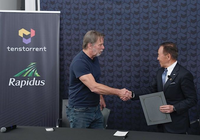
Tenstorrent this week announced that it had signed a deal to license out its RISC-V CPU and AI processor IP to Japan's Leading-edge Semiconductor Technology Center (LSTC), which will use the technology to build its edge-focused AI accelerator. The most curious part of the announcement is that this accelerator will rely on a multi-chiplet design and the chiplets will be made by Japan's Rapidus on its 2nm fabrication process, and then will be packaged by the same company.

Under the terms of the agreement, Tenstorrent will license its datacenter-grade Ascalon general-purpose processor IP to LSTC and will help to implement the chiplet using Rapidus's 2nm fabrication process. Tenstorrent's Ascalon is a high-performance out-of-order RISC-V CPU design that features an eight-wide decoding. The Ascalon core packs six ALUs, two FPUs, and two 256-bit vector units and when combined with a 2nm-class process technology promises to offer quite formidable performance.

The Ascalon was developed by a team led by legendary CPU designer Jim Keller, the current chief executive of Tenstorrent, who used to work on successful projects by AMD, Apple, Intel, and Tesla.

In addition to general-purpose CPU IP licensing, Tenstorrent will co-design 'the chip that will redefine AI performance in Japan.' This apparently means that Tenstorrent  does not plan to license LSTC its proprietary  Tensix cores tailored for neural network inference and training, but will help to design a proprietary AI accelerator generally for inference workloads.

"The joint effort by Tenstorrent and LSTC to create a chiplet-based edge AI accelerator represents a groundbreaking venture into the first cross-organizational chiplet development in semiconductor industry," said Wei-Han Lien, Chief Architect of Tenstorrent's RISC-V products. "The edge AI accelerator will incorporate LSTC's AI chiplet along with Tenstorrent's RISC-V and peripheral chiplet technology. This pioneering strategy harnesses the collective capabilities of both organizations to use the adaptable and efficient nature of chiplet technology to meet the increasing needs of AI applications at the edge."

Rapidus aims to start production of chips on its 2nm fabrication process that is currently under development sometimes in 2027, at least a year behind TSMC and a couple of years behind Intel. Yet, if it starts high-volume 2nm manufacturing in 2027, it will be a major breakthrough from Japan, which is trying hard to return to the global semiconductor leaders.

Building an edge AI accelerator based on Tenstorrent's IP and Rapidus's 2nm-class production node is a big deal for LSTC, Tenstorrent, and Rapidus as it is a testament for technologies developed by these three companies.

"I am very pleased that this collaboration started as an actual project from the MOC conclusion with Tenstorrent last November," said Atsuyoshi Koike, president and CEO of Rapidus Corporation. "We will cooperate not only in the front-end process but also in the chiplet (back-end process), and work on as a leading example of our business model that realizes everything from design to back-end process in a shorter period of time ever."

  • ✇AnandTech
  • Intel Brings vPro to 14th Gen Desktop and Core Ultra Mobile Platforms for Enterprise
    As part of this week's MWC 2024 conference, Intel is announcing that it is adding support for its vPro security technologies to select 14th Generation Core series processors (Raptor Lake-R) and their latest Meteor Lake-based Core Ultra-H and U series mobile processors. As we've seen from more launches than we care to count of Intel's desktop and mobile platforms, they typically roll out their vPro platforms sometime after they've released their full stack of processors, including overclockable K
     

Intel Brings vPro to 14th Gen Desktop and Core Ultra Mobile Platforms for Enterprise

27. Únor 2024 v 17:00

As part of this week's MWC 2024 conference, Intel is announcing that it is adding support for its vPro security technologies to select 14th Generation Core series processors (Raptor Lake-R) and their latest Meteor Lake-based Core Ultra-H and U series mobile processors. As we've seen from more launches than we care to count of Intel's desktop and mobile platforms, they typically roll out their vPro platforms sometime after they've released their full stack of processors, including overclockable K series SKUs and lower-powered T series SKUs, and this year is no exception. Altogether, Intel is announcing vPro Essential and vPro Enterprise support for several 14th Gen Core series SKUs and Intel Core Ultra mobile SKUs.

While Intel's vPro security features aren't anything that we haven't seen before – and on that note, there is nothing new to this generation of vPro technologies – it simply adds existing vPro support, both the total Enterprise securities and the cut-down Essentials vPro hardware-level security to select 14th Gen Core series processors, as well as their latest mobile-focused Meteor Lake processors with Arc graphics launched last year.

Intel 14th Gen vPro: Raptor Lake-R Gets Secured

As we've seen over the last few years with a global shift towards remote work due to the Coronavirus pandemic, the need for up-to-date security in small and larger enterprises is just as critical as it has ever been. Remote and employees in offices alike must have access to the latest software and hardware frameworks to ensure the security of vital data, and that's where Intel vPro comes in.

To quickly recap the current state of affairs, let's take a look at the two levels of Intel vPro securities available,  vPro Essentials and vPro Enterprise, and how they differ.

Intel's vPro Essentials was first launched back in 2022 and is a subset of Intel's complete vPro package, which is now commonly known as vPro Enterprise. The Intel vPro Essentials security package is essentially (as per the name) tailored and designed for small businesses, providing a solid foundation in security without penalizing performance. It integrates hardware-enhanced security features, ensuring hardware-level protection against emerging threats from right from its installation. It also utilizes real-time intelligence for workload optimization and Intel's Thread Detection Technology. It adds an additional layer below the operating system that uses AI-based threat detection to mitigate OS-level threats and attacks.

Pivoting to Intel vPro Enterprise security features, this is designed for SMEs to meet the high demands of large-scale business environments. It offers advanced security features and remote management capabilities, which are crucial for businesses operating with sensitive data and requiring high levels of cybersecurity. Additionally, the platform provides enhanced performance and reliability, making it suitable for intensive workloads and multitasking in a professional setting. Integrating these features from the vPro Enterprise platform ensures that large enterprises can maintain high productivity levels while ensuring data security and efficient IT management with the latest generations of processors, such as the Intel Core 14th Gen family.

Much like we saw when Intel announced their vPro for the 13th Gen Core series, it's worth noting that both the 14th and 13th Gen Core series are based on the same Raptor Lake architecture and, as such, are identical in every aspect bar base and turbo core frequencies.

Intel 14th Gen Core with vPro for Desktop
(Raptor Lake-R)
AnandTech Cores
P+E/T
P-Core
Base/Turbo
(MHz)
E-Core
Base/Turbo
(MHz)
L3 Cache
(MB)
Base
W
Turbo
W
vPRO
Support
(Ent/Ess)
Price
($)
i9-14900K 8+16/32 3200 / 6000 2400 / 4400 36 125 253 Enterprise $589
i9-14900 8+16/32 2000 / 5600 1500 / 4300 36 65 219 Both $549
i9-14900T 8+16/32 1100 / 5500 800 / 4000 36 35 106 Both $549
 
i7-14700K 8+12/28 3400 / 5600 2500 / 4300 33 125 253 Enterprise $409
i7-14700 8+12/28 2100 / 5400 1500 / 4200 33 65 219 Both $384
i7-14700T 8+12/28 1300 / 5000 900 / 3700 33 35 106 Both $384
 
i5-14600K 6+8/20 3500 / 5300 2600 / 4000 24 125 181 Enterprise $319
i5-14600 6+8/20 2700 / 5200 2000 / 3900 24 65 154 Both $255
i5-14500 6+8/20 2600 / 5000 1900 / 3700 24 65 154 Both $232
i5-14600T 6+8/20 1800 / 5100 1200 / 3600 24 35 92 Both $255
i5-14500T 6+8/20 1700 / 4800 1200 / 3400 24 35 92 Both $232

While Intel isn't technically launching any new chip SKUs (either desktop or mobile) with vPro support, the vPro desktop platform features are enabled through the use of specific motherboard chipsets, with both Q670 and W680 chipsets offering sole support for vPro on 14th Gen. Unless users are using either a Q670 or W680 motherboard with the specific chips listed above. vPro Essentials or Enterprise will not be enabled or work with each processor unless installed into a motherboard from one of these chipsets.

As with the previous 13th Gen Core series family (Raptor Lake), the 14th Gen, which is a direct refresh of these, follows a similar pattern. Specific SKUs from the 14th Gen family include support only for the full-fledged vPro Enterprise, including the Core i5-14600K, the Core i7-14700K, and the flagship Core i9-14900K. Intel's vPro Enterprise security features are supported on both Q670 and W680 motherboards, giving users more choice in which board they opt for.

The rest of the above Intel 14th Gen Core series stack, including the non-monikered chips, e.g., the Core i5-14600, as well as the T series, which are optimized for efficient workloads with a lower TDP than the rest of the stack, all support both vPro Enterprise and vPro Essentials. This includes two processors from the Core i9 family, including the Core i9-14900 and Core i9-14900T, two from the i7 series, the Core i7-14700 and Core i7-14700T, and four from the i5 series, the Core i5-14600, Core i5-14500, the Core i5-14600T and the COre i5-14500T.


The ASRock Industrial IMB-X1231 W680 mini-ITX motherboard supports vPro Enterprise and Essentials

For the processors mentioned above (non-K), different levels of vPro support are offered depending on the motherboard chipset. If a user wishes to use a Q670 motherboard, then users can specifically opt to use Intel's cut-down vPro Essentials security features. Intel states that users with a Q670 or W680 can use the full vPro Enterprise security features, including the Core i9-14900K, the Core i7-14700K, and the Core i5-14600K. Outside of this, none of the 14th Gen SKUs with the KF (unlocked with no iGPU) and F (no iGPU) monikers are listed with support for vPro.

Intel Meteor Lake with vPro: Core Ultra H and U Series get Varied vPro Support

Further to the Intel 14th Gen Core series for desktops, Intel has also enabled vPro support for their latest Meteor Lake-based Core Ultra H and U series mobile processors. Unlike the desktop platform for vPro, things are a little different in the mobile space, as Intel offers vPro on their mobile SKUs, either with vPro Enterprise or vPro Essentials, not both.

Intel Core Ultra H and U-Series Processors with vPro
(Meteor Lake)
AnandTech Cores
(P+E+LP/T)
P-Core Turbo
Freq
E-Core Turbo
Freq
GPU GPU Freq L3 Cache
(MB)
vPro Support
(Ent/Ess)
Base TDP Turbo TDP
Ultra 9  
Core Ultra 9 185H 6+8+2/22 5100 3800 Arc Xe (8) 2350 24 Enterprise 45 W 115 W
Ultra 7  
Core Ultra 7 165H 6+8+2/22 5000 3800 Arc Xe (8) 2300 24 Enterprise 28 W 64/115 W
Core Ultra 7 155H 6+8+2/22 4800 3800 Arc Xe (8) 2250 24 Essentials 28 W 64/115 W
Core Ultra 7 165U 2+8+2/14 4900 3800 Arc Xe (4) 2000 12 Enterprise 15 W 57 W
Core Ultra 7 164U 2+8+2/14 4800 3800 Arc Xe (4) 1800 12 Enterprise 9 W 30 W
Core Ultra 7 155U 2+8+2/14 4800 3800 Arc Xe (4) 1950 12 Essentials 15 W 57 W
Ultra 5  
Core Ultra 5 135H 4+8+2/18 4600 3600 Arc Xe
(7)
2200 18 Enterprise 28 W 64/115 W
Core Ultra 5 125H 4+8+2/18 4500 3600 Arc Xe (7) 2200 18 Essentials 28 W 64/115 W
Core Ultra 5 135U 2+8+2/14 4400 3600 Arc Xe (4) 1900 12 Enterprise 15 W 57 W
Core Ultra 5 134U 2+8+2/14 4400 3800 Arc Xe (4) 1750 12 Enterprise 9 W 30 W
Core Ultra 5 125U 2+8+2/14 4300 3600 Arc Xe (4) 1850 12 Essentials 15 W 57 W

The above table highlights not just the specifications of each Core Ultra 9, 7, and 5 SKU but also denotes which model gets what level of vPro support. Starting with the Core Ultra 9 185H processor, the current mobile flagship chip on Meteor Lake, this chip supports vPro Enterprise. Along with the other top-tier SKU from each of the Core Ultra 9, 7, and 5 families, including the Core Ultra 7 165H and the Core Ultra 135H, other chips with vPro Enterprise support include the Core Ultra 7 165U and Core Ultra 7 164U, as well as the Core Ultra 5 135U and Core Ultra 5 134U.

Intel's other Meteor Lake chips, including the Core Ultra 7 155H, the Core Ultra 7 155U, the Core Ultra 5 125H, and the Core Ultra 5 125U, only support Intel's vPro Essentials security features. This presents a slight 'dropping of the ball' from Intel on this, which we highlighted in our Intel 13th Gen Core gets vPro piece last year.

Intel vPro Support Announcement With No New Hardware, Why Announce Later?

It is worth noting that Intel's announcement of adding vPro support to their first launch of Meteor Lake Core Ultra SKUs isn't entirely new; Intel did highlight that Meteor Lake would support vPro last year within their Series 1 Product Brief dated 12/20/2023. Intel's formal announcement of vPro support for Meteor Lake is more about which SKU has which level of support, and we feel this could pose problems to users who have already purchased Core Ultra series notebooks for business and enterprise use. Multiple outlets, including Newegg and directly from HP, are alluding to mentioning vPro whatsoever.

This could mean that a user has purchased a notebook with, say, a Core Ultra 5 125H (vPro Essentials), which would be used within an SME or by said SME as a bulk purchase but wouldn't be aware that the chip doesn't have vPro Enterprise, from which they personally and from a business standpoint could benefit from the additional securities. We reached out to Intel, and they sent us the following statement.

"Since we are launching vPro powered by Intel Core Ultra & Intel Core 14th Gen this week, prospective buyers will begin seeing the relevant system information on OEM and enterprise retail partner (eg. CDW) websites in the weeks ahead. This will include information on whether a system is equipped with vPro Enterprise or Essentials so that they can purchase the right system for their compute needs."

  • ✇AnandTech
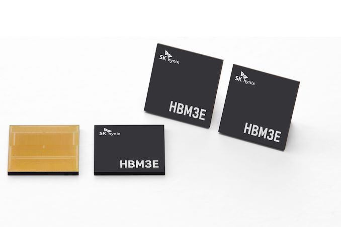
  • Samsung Launches 12-Hi 36GB HBM3E Memory Stacks with 10 GT/s Speed
    Samsung announced late on Monday the completion of the development of its 12-Hi 36 GB HBM3E memory stacks, just hours after Micron said it had kicked off mass production of its 8-Hi 24 GB HBM3E memory products. The new memory packages, codenamed Shinebolt, increase peak bandwidth and capacity compared to their predecessors, codenamed Icebolt, by over 50% and are currently the world's fastest memory devices. As the description suggests, Samsung's Shinebolt 12-Hi 36 GB HBM3E stacks pack 12 24Gb m
     

Samsung Launches 12-Hi 36GB HBM3E Memory Stacks with 10 GT/s Speed

27. Únor 2024 v 13:00

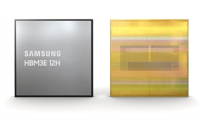
Samsung announced late on Monday the completion of the development of its 12-Hi 36 GB HBM3E memory stacks, just hours after Micron said it had kicked off mass production of its 8-Hi 24 GB HBM3E memory products. The new memory packages, codenamed Shinebolt, increase peak bandwidth and capacity compared to their predecessors, codenamed Icebolt, by over 50% and are currently the world's fastest memory devices.

As the description suggests, Samsung's Shinebolt 12-Hi 36 GB HBM3E stacks pack 12 24Gb memory devices on top of a logic die featuring a 1024-bit interface. The new 36 GB HBM3E memory modules feature a data transfer rate of 10 GT/s and thus offer a peak bandwidth of 1.28 TB/s per stack, the industry's highest per-device (or rather per-module) memory bandwidth.

Meanwhile, keep in mind that developers of HBM-supporting processors tend to be cautious, so they will use Samsung's HBM3E at much lower data transfer rates to some degree because of power consumption and to some degree to ensure ultimate stability for artificial intelligence (AI) and high-performance computing (HPC) applications.

Samsung HBM Memory Generations
  HBM3E
(Shinebolt)
HBM3
(Icebolt)
HBM2E
(Flashbolt)
HBM2
(Aquabolt)
Max Capacity 36GB 24 GB 16 GB 8 GB
Max Bandwidth Per Pin 9.8 Gb/s 6.4 Gb/s 3.6 Gb/s 2.0 Gb/s
Number of DRAM ICs per Stack 12 12 8 8
Effective Bus Width 1024-bit
Voltage ? 1.1 V 1.2 V 1.2 V
Bandwidth per Stack 1.225 TB/s 819.2 GB/s 460.8 GB/s 256 GB/s

To make its Shinebolt 12-Hi 36 GB HBM3E memory stacks, Samsung had to use several advanced technologies. First, the 36 GB HBM3E memory products are based on memory devices made on Samsung's 4th generation 10nm-class (14nm) fabrication technology, which is called and uses extreme ultraviolet (EUV) lithography.

Secondly, to ensure that 12-Hi HBM3E stacks have the same z-height as 8-Hi HBM3 products, Samsung used its advanced thermal compression non-conductive film (TC NCF), which allowed it to achieve the industry's smallest gap between memory devices at seven micrometers (7 µm). By shrinking gaps between DRAMs, Samsung increases vertical density and mitigates chip die warping. Furthermore, Samsung uses bumps of various sizes between the DRAM ICs; smaller bumps are used in areas for signaling. In contrast, larger ones are placed in spots that require heat dissipation, which improves thermal management.

Samsung estimates that its 12-Hi HBM3E 36 GB modules can increase the average speed for AI training by 34% and expand the number of simultaneous users of inference services by more than 11.5 times. However, the company has not elaborated on the size of the LLM.

Samsung has already begun providing samples of the HBM3E 12H to customers, with mass production scheduled to commence in the first half of this year.

Source: Samsung

  • ✇AnandTech
  • Micron Kicks Off Production of HBM3E Memory
    Micron Technology on Monday said that it had initiated volume production of its HBM3E memory. The company's HBM3E known good stack dies (KGSDs) will be used for Nvidia's H200 compute GPU for artificial intelligence (AI) and high-performance computing (HPC) applications, which will ship in the second quarter of 2024. Micron has announced it is mass-producing 24 GB 8-Hi HBM3E devices with a data transfer rate of 9.2 GT/s and a peak memory bandwidth of over 1.2 TB/s per device. Compared to HBM3, H
     

Micron Kicks Off Production of HBM3E Memory

26. Únor 2024 v 18:00

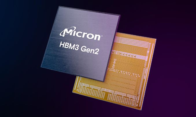
Micron Technology on Monday said that it had initiated volume production of its HBM3E memory. The company's HBM3E known good stack dies (KGSDs) will be used for Nvidia's H200 compute GPU for artificial intelligence (AI) and high-performance computing (HPC) applications, which will ship in the second quarter of 2024.

Micron has announced it is mass-producing 24 GB 8-Hi HBM3E devices with a data transfer rate of 9.2 GT/s and a peak memory bandwidth of over 1.2 TB/s per device. Compared to HBM3, HBM3E increases data transfer rate and peak memory bandwidth by a whopping 44%, which is particularly important for bandwidth-hungry processors like Nvidia's H200.

Nvidia's H200 product relies on the Hopper architecture and offers the same computing performance as the H100. Meanwhile, it is equipped with 141 GB of HBM3E memory featuring bandwidth of up to 4.8 TB/s, a significant upgrade from 80 GB of HBM3 and up to 3.35 TB/s bandwidth in the case of the H100.

Micron's memory roadmap for AI is further solidified with the upcoming release of a 36 GB 12-Hi HBM3E product in March 2024. Meanwhile, it remains to be seen where those devices will be used.

Micron uses its 1β (1-beta) process technology to produce its HBM3E, which is a significant achievement for the company as it uses its latest production node for its data center-grade products, which is a testament to the manufacturing technology.

Starting mass production of HBM3E memory ahead of competitors SK Hynix and Samsung is a significant achievement for Micron, which currently holds a 10% market share in the HBM sector. This move is crucial for the company, as it allows Micron to introduce a premium product earlier than its rivals, potentially increasing its revenue and profit margins while gaining a larger market share.

"Micron is delivering a trifecta with this HBM3E milestone: time-to-market leadership, best-in-class industry performance, and a differentiated power efficiency profile," said Sumit Sadana, executive vice president and chief business officer at Micron Technology. "AI workloads are heavily reliant on memory bandwidth and capacity, and Micron is very well-positioned to support the significant AI growth ahead through our industry-leading HBM3E and HBM4 roadmap, as well as our full portfolio of DRAM and NAND solutions for AI applications."

Source: Micron

  • ✇AnandTech
  • Intel Previews Sierra Forest with 288 E-Cores, Announces Granite Rapids-D for 2025 Launch at MWC 2024
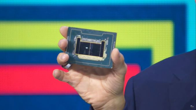
    At MWC 2024, Intel confirmed that Granite Rapids-D, the successor to Ice Lake-D processors, will come to market sometime in 2025. Furthermore, Intel also provided an update on the 6th Gen Xeon Family, codenamed Sierra Forest, which is set to launch later this year and will feature up to 288 cores designed for vRAN network operators to improve performance in boost per rack for 5G workloads. These chips are designed for handling infrastructure, applications, and AI workloads and aim to capitalize
     

Intel Previews Sierra Forest with 288 E-Cores, Announces Granite Rapids-D for 2025 Launch at MWC 2024

26. Únor 2024 v 13:25

At MWC 2024, Intel confirmed that Granite Rapids-D, the successor to Ice Lake-D processors, will come to market sometime in 2025. Furthermore, Intel also provided an update on the 6th Gen Xeon Family, codenamed Sierra Forest, which is set to launch later this year and will feature up to 288 cores designed for vRAN network operators to improve performance in boost per rack for 5G workloads.

These chips are designed for handling infrastructure, applications, and AI workloads and aim to capitalize on current and future AI and automation opportunities, enhancing operational efficiency and ownership costs in next-gen applications and reflecting Intel's vision of integrating 'AI Everywhere' across various infrastructures.

Intel Sierra Forest: Up to 288 Efficiency Cores, Set for 2H 2024

The first of Intel's announcements at MWC 2024 focuses on their upcoming Sierra Forest platform, which is scheduled for the 1st half of 2024. Initially announced in February 2022 during Intel's Investor Meeting, Intel is splitting its server roadmap into solutions featuring only performance (P) and efficiency (E) cores. We already know that Sierra Forest's new chips feature a full E-core architecture designed for maximum efficiency in scale-out, cloud-native, and contained environments.

These chips utilize CPU chiplets built on the Intel 3 process alongside twin I/O chiplets based on the Intel 7 node. This combination allows for a scalable architecture, which can accommodate increasing core counts by adding more chiplets, optimizing performance for complex computing environments.

Intel's Sierra Forest, Intel's full E-core designed Xeon processor family, is anticipated to significantly enhance power efficiency with up to 288 E-cores per socket. Intel also claims that Sierra Forest is expected to deliver 2.7 times the performance-per-rack compared to an unspecified platform from 2021; this could be either Ice Lake or Cascade Lake, but Intel didn't mention which.

Additionally, Intel is promising savings of up to 30% in Infrastructure Power Management with Sierra Forest as their Infrastructure Power Manager (IPM) application is now available commercially for 5G cores. Power manageability and efficiency are growing challenges for network operators, so IPM is designed to allow network operators to optimize energy efficiency and TCO savings.

Intel also includes vRAN, which is vital for modern mobile networks, and many operators are forgoing opting for specific hardware and instead leaning towards virtualized radio access networks (vRANs). Using vRAN Boost, which is an integrated accelerator within Xeon Processors, Intel states that the 4th Gen Xeon should be able to reduce power consumption by around 20% while doubling the available network capacity.

Intel's push for 'AI Everywhere' is also a constant focus here, with AI's role in vRAN management becoming more crucial. Intel has announced the vRAN AI Developer Kit, which is available to select partners. This allows partners and 5G network providers to develop AI models to optimize for vRAN applications, tailor their vRAN-based functions to more use cases, and adapt to changes within those scenarios.

Intel Granite Rapids-D: Coming in 2025 For Edge Solutions

Intel's Granite Rapids-D, designed for Edge solutions, is set to bolster Intel's role in virtual radio access network (vRAN) workloads in 2025. Intel also promises marked efficiency enhancements and some vRAN Boost optimizations similar to those expected on Sierra Forest. Set to follow on from the current Ice Lake-D for the edge; Intel is expected to use the performance (P) cores used within Granite Rapids server parts and optimize the V/F curve designed for the lower-powered Edge platform. As outlined by Intel, the previous 4th generation Xeon platform effectively doubled vRAN capacity, enhancing network capabilities while reducing power consumption by up to 20%.

Granite Rapids-D aims to further these advancements, utilizing Intel AVX for vRAN and integrated Intel vRAN Boost acceleration, thereby offering substantial cost and performance benefits on a global scale. While Intel hasn't provided a specific date (or month) of when we can expect to see Granite Rapids-D in 2025, Intel is currently in the process of sampling these next-gen Xeon-D processors with partners, aiming to ensure a market-ready platform at launch.

Related Reading

  • ✇AnandTech
  • AMD Fixed the STAPM Throttling Issue, So We Retested The Ryzen 7 8700G and Ryzen 5 8600G
    When we initially reviewed the latest Ryzen 8000G APUs from AMD last month, the Ryzen 7 8700G and Ryzen 5 8600G, we became aware of an issue that caused the APUs to throttle after a few minutes. This posed an issue for a couple of reasons, the first being it compromised our data to reflect the true capabilities of the processors, and the second, it highlighted an issue that AMD forgot to disable from their mobile series of Pheonix chips (Ryzen 7040) when implementing it over to the desktop. We
     

AMD Fixed the STAPM Throttling Issue, So We Retested The Ryzen 7 8700G and Ryzen 5 8600G

23. Únor 2024 v 14:00

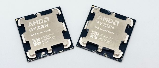
When we initially reviewed the latest Ryzen 8000G APUs from AMD last month, the Ryzen 7 8700G and Ryzen 5 8600G, we became aware of an issue that caused the APUs to throttle after a few minutes. This posed an issue for a couple of reasons, the first being it compromised our data to reflect the true capabilities of the processors, and the second, it highlighted an issue that AMD forgot to disable from their mobile series of Pheonix chips (Ryzen 7040) when implementing it over to the desktop.

We updated the data in our review of the Ryzen 7 8700G and Ryzen 5 8600G to reflect performance with STAPM on the initial firmware and with STAPM removed with the latest firmware. Our updated and full review can be accessed by clicking the link below:

As we highlighted in our Ryzen 8000G APU STAPM Throttling article, AMD, through AM5 motherboard vendors such as ASUS, has implemented updated firmware that removes the STAPM limitation. Just to quickly recap the Skin Temperature-Aware Power Management (STAPM) feature and what it does, AMD introduced it in 2014. STAPM itself is a feature implemented into their mobile processors. It is designed to extend the on-die power management by considering the processor's internal temperatures taken by on-chip thermal diodes and the laptop's surface temperature (i.e., the skin temperature).

The aim of STAPM is to prevent laptops from becoming uncomfortably warm for users, allowing the processor to actively throttle back its heat generation based on the thermal parameters between the chassis and the processor itself. The fundamental issue with STAPM in the case of the Ryzen 8000G APUs, including the Ryzen 7 8700G and Ryzen 5 8600G, is that these are mobile processors packaged into a format for use with the AM5 desktop platform. As a desktop platform is built into a chassis that isn't placed on a user's lap, the STAPM feature becomes irrelevant.

As we saw when we ran a gaming load over a prolonged period of time on the Ryzen 7 8700G with the firmware available at launch, we hit power throttling (STAPM) after around 3 minutes. As we can see in the above chart, power dropped from a sustained value of 83-84 W down to around 65 W, representing a drop in power of around 22%. While we know Zen 4 is a very efficient architecture at lower power values, overall performance will drop once this limit is hit. Unfortunately, AMD forgot to remove STAPM limits when transitioning Pheonix to the AM5 platform.

Retesting the same game (F1 2023) at the same settings (720p High) with the firmware highlighting that STAPM had been removed, we can see that we aren't experiencing any of the power throttling we initially saw. We can see power is sustained for over 10 minutes of testing (we did test for double this), and we saw no drops in package power, at least not from anything related to STAPM. This means for users on the latest firmware on whatever AM5 motherboard is being used, power and, ultimately, performance remain consistent with what the Ryzen 7 8700G should have been getting at launch.

The key question is, does removing the STAPM impact our initial results in our review of the Ryzen 7 8700G and Ryzen 5 8600G? And if so, by how much, or if at all? We added the new data to our review of the Ryzen 7 8700G and Ryzen 5 8600G but kept the initial results so that users can see if there are any differences in performance. Ultimately, benchmark runs are limited to the time it takes to run them, but in real-world scenarios, tasks such as video rendering and longer sustained loads are more likely to show gains in performance. After all, a drop of 22% in power is considerable, especially over a task that could take an hour.

(4-1d) Blender 3.6: Pabellon Barcelona (CPU Only)

Using one of our longer benchmarks, such as Blender 3.6, to highlight where performance gains are notable when using the latest firmware with the STAPM limitations removed, we saw an increase in performance of around 7.5% on the Ryzen 7 8700G with this removed. In the same benchmark, we saw an increase of around 4% on the Ryzen 5 8600G APU.

Over all of the Blender 3.6 tests in the rendering section of our CPU performance suite, performance gains hovered between 2 and 4.4% on the Ryzen 5 8600G, and between 5 and 7.5% on the Ryzen 8700G, which isn't really free performance, it's the performance that should have been there to begin with at launch.

IGP World of Tanks - 768p Min - Average FPS

Looking at how STAPM affected our initial data, we can see that the difference in World of Tanks at 768p Minumum settings had a marginal effect at best through STAPM by around 1%. Given how CPU-intensive World of Tanks is, and combining this with integrated graphics, the AMD Ryzen APUs (5000G and 8000G) both shine compared to Intel's integrated UHD graphics in gaming. Given that gaming benchmarks are typically time-limited runs, it's harder to identify performance gains. The key to takeaway here is that with the STAPM limitation removed, the performance shouldn't drop over sustained periods of time, so our figures above and our updated review data aren't compromised.

(i-3) Total War Warhammer 3 - 1440p Ultra - Average FPS

Regarding gaming with a discrete graphics card, we saw no drastic changes in performance, as highlighted by our Total War Warhammer 3 at 1440p Ultra benchmark. Across the board, in our discrete graphics results with both the Ryzen 7 8700G and the Ryzen 5 8600G, we saw nothing but marginal differences in performance (less than 1%). As we've mentioned, removing the STAPM limitations doesn't necessarily improve performance. Still, it allows the APUs to keep the same performance level for sustained periods, which is how it should have been at launch. With STAPM applied as with the initial firmware at launch on AM5 motherboards, power would drop by around 22%, limiting the full performance capability over prolonged periods.

As we've mentioned, we have updated our full review of the AMD Ryzen 7 8700G and Ryzen 5 8600G APUs to reflect our latest data gathered from testing on the latest firmware. Still, we can fully confirm that the STAPM issue has been fixed and that the performance is as it should be on both chips.

You can access all of our updated data in our review of the Ryzen 7 8700G and Ryzen 5 8600G by clicking the link below.

  • ✇AnandTech
  • AMD CEO Dr. Lisa Su to Deliver Opening Keynote at Computex 2024
    Taiwan External Trade Development Council (TAITRA), the organizer of Computex, announced today that Dr. Lisa Su, AMD's chief executive officer, will give the trade show's Opening Keynote. Su's speech is set for the morning of June 3, 2024, shortly before the formal start of the show. According to AMD, the keynote talk will be "highlighting the next generation of AMD products enabling new experiences and breakthrough AI capabilities from the cloud to the edge, PCs and intelligent end devices." T
     

AMD CEO Dr. Lisa Su to Deliver Opening Keynote at Computex 2024

22. Únor 2024 v 21:00

Taiwan External Trade Development Council (TAITRA), the organizer of Computex, announced today that Dr. Lisa Su, AMD's chief executive officer, will give the trade show's Opening Keynote. Su's speech is set for the morning of June 3, 2024, shortly before the formal start of the show. According to AMD, the keynote talk will be "highlighting the next generation of AMD products enabling new experiences and breakthrough AI capabilities from the cloud to the edge, PCs and intelligent end devices."

This year's Computex is focused on six key areas: AI computing, Advanced Connectivity, Future Mobility, Immersive Reality, Sustainability, and Innovations. Being a leading developer of CPUs, AI and HPC GPUs, consumer GPUs, and DPUs, AMD can talk most of these topics quite applicably.

As AMD is already mid-cycle on most of their product architectures, the company's most recent public roadmaps have them set to deliver major new CPU and GPU architectures before the end of 2024 with Zen 5 CPUs and RDNA 4 GPUs, respectively. AMD has not previously given any finer guidance on when in the year to expect this hardware, though AMD's overall plans for 2024 are notably more aggressive than the start of their last architecture cycle in 2022. Of note, the company has previously indicated that it intends to launch all 3 flavors of the Zen 5 architecture this year – not just the basic core, but also Zen 5c and Zen 5 with V-Cache – as well as a new mobile SoC (Strix Point). By comparison, it took AMD well into 2023 to do the same with Zen 4 after starting with a fall 2022 launch for those first products.


AMD 2022 Financial Analyst Day CPU Core Roadmap

This upcoming keynote will be Lisa Su's third Computex keynote after her speeches at Computex 2019 and Computex 2022. In both cases she also announced upcoming AMD products.

In 2019, she showcased performance improvements of then upcoming 3rd Generation Ryzen desktop processors and 7nm EPYC datacenter processors. Lisa Su also highlighted AMD's advancements in 7nm process technology, showcasing the world's first 7nm gaming GPU, the Radeon VII, and the first 7nm datacenter GPU, the Radeon Instinct MI60.

In 2022, the head of AMD offered a sneak peek at the then-upcoming Ryzen 7000-series desktop processors based on the Zen 4 architecture, promising significant performance improvements. She also teased the next generation of Radeon RX 7000-series GPUs with the RDNA 3 architecture.

  • ✇AnandTech
  • Arm and Samsung to Co-Develop 2nm GAA-Optimized Cortex Cores
    Arm and Samsung this week announced their joint design-technology co-optimization (DTCO) program for Arm's next-generation Cortex general-purpose CPU cores as well as Samsung's next-generation process technology featuring gate-all-around (GAA) multi-bridge-channel field-effect transistors (MBCFETs).  "Optimizing Cortex-X and Cortex-A processors on the latest Samsung process node underscores our shared vision to redefine what’s possible in mobile computing, and we look forward to continuing to p
     

Arm and Samsung to Co-Develop 2nm GAA-Optimized Cortex Cores

22. Únor 2024 v 13:00

Arm and Samsung this week announced their joint design-technology co-optimization (DTCO) program for Arm's next-generation Cortex general-purpose CPU cores as well as Samsung's next-generation process technology featuring gate-all-around (GAA) multi-bridge-channel field-effect transistors (MBCFETs). 

"Optimizing Cortex-X and Cortex-A processors on the latest Samsung process node underscores our shared vision to redefine what’s possible in mobile computing, and we look forward to continuing to push boundaries to meet the relentless performance and efficiency demands of the AI era," said Chris Bergey, SVP and GM, Client Business at Arm.

Under the program, the companies aim to deliver tailored versions of Cortex-A and Cortex-X cores made on Samsung's 2 nm-class process technology for various applications, including smartphones, datacenters, infrastructure, and various customized system-on-chips. For now, the companies does not say whether they aim to co-optimize Arm's Cortex cores for Samsung's 1st generation 2 nm production node called SF2 (due in 2025), or the plan is to optimize these cores for all SF2-series technologies, including SF2 and SF2P.

GAA nanosheet transistors with channels that are surrounded by gates on all four sides have a lot of options for optimization. For example, nanosheet channels can be widened to increase drive current and boost performance or shrunken to reduce power consumption and cost. Depending on the application, Arm and Samsung will have plenty of design choices.

Keeping in mind that we are talking about Cortex-A cores aimed at a wide variety of applications as well as Cortex-X cores designed specifically to deliver maximum performance, the results of the collaborative work promise to be quite decent. In particular, we are looking forward Cortex-X cores with maximized performance, Cortex-A cores with optimized performance and power consumption, and Cortex-A cores with reduced power consumption.

Nowadays collaboration between IP (intellectual property) developers, such as Arm, and foundries, such as Samsung Foundry, is essential to maximize performance, reduce power consumption, and optimize transistor density. The joint work with Arm will ensure that Samsung's foundry partners will have access to processor cores that can deliver exactly what they need.

  • ✇AnandTech
  • IFS Reborn as Intel Foundry: Expanded Foundry Business Adds 14A Process To Roadmap
    5 nodes in 4 years. This is what Intel CEO Pat Gelsinger promised Intel’s customers, investors, and the world at large back in 2021, when he laid out Intel’s ambitious plan to regain leadership in the foundry space. After losing Intel’s long-held spot as the top fab in the world thanks to compounding delays in the 2010s, the then-new Intel CEO bucked calls from investors to sell off Intel’s fabs, and instead go all-in on fabs like Intel has never done before, to become a top-to-bottom foundry se
     

IFS Reborn as Intel Foundry: Expanded Foundry Business Adds 14A Process To Roadmap

21. Únor 2024 v 16:30

5 nodes in 4 years. This is what Intel CEO Pat Gelsinger promised Intel’s customers, investors, and the world at large back in 2021, when he laid out Intel’s ambitious plan to regain leadership in the foundry space. After losing Intel’s long-held spot as the top fab in the world thanks to compounding delays in the 2010s, the then-new Intel CEO bucked calls from investors to sell off Intel’s fabs, and instead go all-in on fabs like Intel has never done before, to become a top-to-bottom foundry service for the entire world to use.

Now a bit over two years later, and Intel is just starting to see the first fruits from that aggressive roadmap, both in terms of technologies and customers. Products based on Intel’s first EUV-based node, Intel 4, are available in the market today, and its high-volume counterpart, Intel 3, is ready as well. Meanwhile, Intel is putting the final touches on its first Gate-All-Around (GAAFET)/RibbonFET for 2024 and 2025. It’s a heady time for the company, but it’s also a critical one. Intel has reached the point where they need to deliver on those promises – and they need to do so in a very visible way.

To that end, today Intel’s Foundry group – the artist formally known as Intel Foundry Services – is holding its first conference, Direct Connect. And even more than being a showcase for customers and press, this is Intel’s coming-out party for the fab industry as a whole, where Intel’s foundry (and only Intel’s foundry) gets the spotlight, a rarity in the massive business that is Intel.

  • ✇AnandTech
  • Arm Announces Neoverse V3 and N3 CPU Cores: Building Bigger and Moving Faster with CSS
    A bit over 5 years ago, Arm announced their Neoverse initiative for server, cloud, and infrastructure CPU cores. Doubling-down on their efforts to break into the infrastructure CPU market in a big way, the company set about an ambitious multi-year plan to develop what would become a trio of CPU core lineups to address different segments of the market – ranging  from the powerful V series to the petite E series core. And while things have gone a little differently than Arm initially projected, th
     

Arm Announces Neoverse V3 and N3 CPU Cores: Building Bigger and Moving Faster with CSS

21. Únor 2024 v 16:00

A bit over 5 years ago, Arm announced their Neoverse initiative for server, cloud, and infrastructure CPU cores. Doubling-down on their efforts to break into the infrastructure CPU market in a big way, the company set about an ambitious multi-year plan to develop what would become a trio of CPU core lineups to address different segments of the market – ranging  from the powerful V series to the petite E series core. And while things have gone a little differently than Arm initially projected, they’re hardly in a position to complain, as the Neoverse line of CPU cores has never been as successful as it is now. Custom CPU designs based on Neoverse cores are all the rage with cloud providers, and the broader infrastructure market has seen its own surge.

Now, as the company and its customers turn towards 2024 and a compute market that is in the throes of another transformative change due to insatiable demand for AI hardware, Arm is preparing to release its next generation of Neoverse CPU core designs to its customers. And in the process, the company is reaching the culmination of the original Neoverse roadmap.

This morning the company is taking the wraps off of the V3 CPU architecture (codename Poseidon) for high-performance systems, as well as the N3 CPU architecture (codename Hermes) for balanced systems. These designs are now ready for customers to begin integrating into their own chip designs, with both the individual CPU core designs as well as the larger Neoverse Compute Subsystems (CSS) available. Between the various combinations of IP configurations, Arm is looking to offer something for everyone, and especially chip designers who are looking to integrate ready-made IP for a quick turnaround in developing their own chips.

With that said, it should be noted that today’s announcement is also a lighter one than what we’ve come to expect from previous Neoverse announcements. Arm isn’t releasing any of the deep architectural details on the new Neoverse platforms today, so while we have the high-level details on the hardware and some basic performance estimates, the underlying details on the CPU cores and their related plumbing is something Arm is keeping to themselves until a later time.

  • ✇AnandTech
  • The Intel IFS Direct Connect 2024 Keynote (Starts at 8:30am PT/16:30 UTC)
    This morning, Intel is set to provide updates on its foundry business (IFS) and process roadmap at its IFS Direct Connect event in Santa Clara. Intel is expected to unveil plans for how the company will transform the foundry industry and how it is set to become the world's first and only fully integrated systems foundry in the AI space. Led by Intel CEO Pat Gelsinger and Stuart Pann, the Senior Vice President and General Manager of Intel Foundry Services, both will deliver the event's opening ke
     

The Intel IFS Direct Connect 2024 Keynote (Starts at 8:30am PT/16:30 UTC)

21. Únor 2024 v 16:00

This morning, Intel is set to provide updates on its foundry business (IFS) and process roadmap at its IFS Direct Connect event in Santa Clara. Intel is expected to unveil plans for how the company will transform the foundry industry and how it is set to become the world's first and only fully integrated systems foundry in the AI space. Led by Intel CEO Pat Gelsinger and Stuart Pann, the Senior Vice President and General Manager of Intel Foundry Services, both will deliver the event's opening keynote. Expected guests throughout the keynote include Sam Altman, the co-founder and CEO of OpenAI, Gina Raimondo, the US Secretary of Commerce, and Satya Nadella, the Chairman and CEO of Microsoft.

Join us at 8:30 am PT/16:30 pm UTC.

  • ✇AnandTech
  • Capsule Review: AlphaCool Apex Stealth Metal 120mm Fan
    Alphacool, a renowned name in the realm of PC cooling solutions, recently launched their Apex Stealth Metal series of cooling fans. Prior to their launch, the new fans had amassed a significant amount of hype in the PC community, in part because of the unfortunate misconception that the entire fan would be made out of metal. Regardless of whether they're made entirely out of metal or not, however, these fans are notable for their unique construction, combining a metallic frame with plastic part
     

Capsule Review: AlphaCool Apex Stealth Metal 120mm Fan

20. Únor 2024 v 14:00

Alphacool, a renowned name in the realm of PC cooling solutions, recently launched their Apex Stealth Metal series of cooling fans. Prior to their launch, the new fans had amassed a significant amount of hype in the PC community, in part because of the unfortunate misconception that the entire fan would be made out of metal.

Regardless of whether they're made entirely out of metal or not, however, these fans are notable for their unique construction, combining a metallic frame with plastic parts that are decoupled from the metal. This design choice not only contributes to the fan's aesthetic appeal but also plays a role in its operational efficiency.

The series includes two distinct models, the Apex Stealth Metal 120 mm and the Apex Stealth Metal Power 120 mm, distinguished primarily by their maximum rotational speeds. The former reaches up to 2000 RPM, while the latter, designed for more demanding applications, can achieve a remarkable 3000 RPM. Available in four color options – White, Matte Black, Chrome, and Gold – these fans offer a blend of style and functionality, making them a versatile choice for various PC builds.

  • ✇AnandTech
  • Crucial T705 Gen5 NVMe SSD: A 14.5 GBps Consumer Flagship with 2400 MT/s 232L NAND
    Crucial is unveiling the latest addition to its Gen5 consumer NVMe SSD lineup today - the T705 PCIe 5.0 M.2 2280 NVMe SSD. It takes over flagship duties from the Crucial T700 released last year. The company has been putting focus on the high-end consumer SSD segment in the last few quarters. The T700 was one of the first to offer more than 12 GBps read speeds, and the T705 being launched today is one of the first drives available for purchase in the 14+ GBps read speeds category. The Crucial T7
     

Crucial T705 Gen5 NVMe SSD: A 14.5 GBps Consumer Flagship with 2400 MT/s 232L NAND

20. Únor 2024 v 14:00

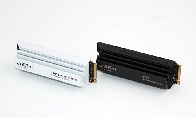
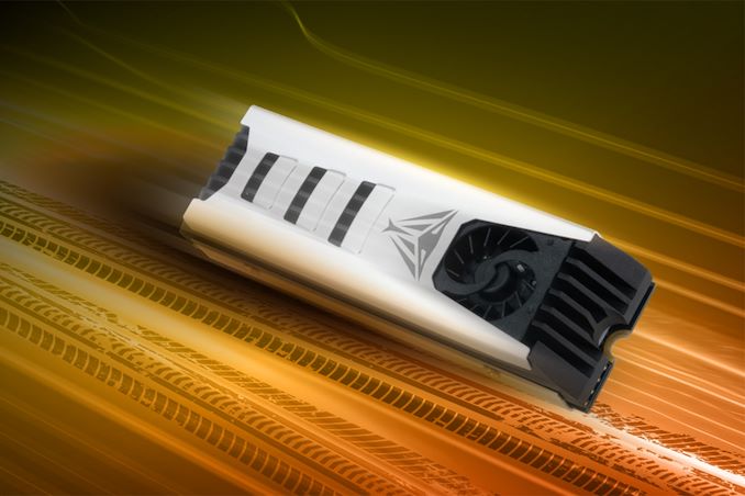
Crucial is unveiling the latest addition to its Gen5 consumer NVMe SSD lineup today - the T705 PCIe 5.0 M.2 2280 NVMe SSD. It takes over flagship duties from the Crucial T700 released last year. The company has been putting focus on the high-end consumer SSD segment in the last few quarters. The T700 was one of the first to offer more than 12 GBps read speeds, and the T705 being launched today is one of the first drives available for purchase in the 14+ GBps read speeds category.

The Crucial T705 utilizes the same platform as the T700 from last year - Phison's E26 controller with Micron's B58R 232L 3D TLC NAND. The key difference is the B58R NAND operating at 2400 MT/s in the new T705 (compared to the 2000 MT/s in the T700). Micron's 232L NAND process has now matured enough for the company to put out 2400 MT/s versions with enough margins. Similar to the T700, this drive is targeted towards gamers, content creators, and professional users as well as data-heavy AI use-cases.

The move to 2400 MT/s NAND has allowed Crucial to claim an increase in the performance of the drive in all four corners - up to 20% faster random writes, and 18% higher sequential reads. Additionally, Crucial also claims more bandwidth in a similar power window for the new drive.

The T705 is launching in three capacities - 1TB, 2TB, and 4TB. Both heatsink and non-heatsink versions are available. Crucial is also offering a white heatsink limited edition for the 2TB version. This caters to users with white-themed motherboards that are increasingly gaining market presence.

Phison has been pushing DirectStorage optimizations in its high-end controllers, and it is no surprise that the T705 advertises the use of Phison's 'I/O+ Technology' to appeal to gamers. Given its high-performance nature, it is no surprise that the E26 controller needs to be equipped with DRAM for managing the flash translation layer (FTL). Crucial is using Micron LPDDR4 DRAM (1GB / TB of flash) in the T705 for this purpose.

Crucial T705 Gen5 NVMe SSD Specifications
Capacity 1 TB 2 TB 4 TB
Model Numbers CT1000T705SSD3 (Non-Heatsink)
CT1000T705SSD5 (Heatsink)
CT2000T705SSD3 (Non-Heatsink)
CT2000T705SSD5 (Black Heatsink)
CT2000T705SSD5A (White Heatsink)
CT4000T705SSD3 (Non-Heatsink)
CT4000T705SSD5 (Heatsink)
Controller Phison PS5026-E26
NAND Flash Micron B58R 232L 3D TLC NAND at 2400 MT/s
Form-Factor, Interface Double-Sided M.2-2280, PCIe 5.0 x4, NVMe 2.0
Sequential Read 13600 MB/s 14500 MB/s 14100 MB/s
Sequential Write 10200 MB/s 12700 MB/s 12600 MB/s
Random Read IOPS 1.4 M 1.55 M 1.5 M
Random Write IOPS 1.75 M 1.8 M 1.8 M
SLC Caching Dynamic (up to 11% of user capacity)
TCG Opal Encryption Yes
Warranty 5 years
Write Endurance 600 TBW
0.33 DWPD
1200 TBW
0.33 DWPD
2400 TBW
0.33 DWPD
MSRP $240 (24¢/GB) (Non- Heatsink)
$260 (26¢/GB) (Heatsink)
$400 (20¢/GB) (Non- Heatsink)
$440 (22¢/GB) (Black Heatsink)
$484 (24.2¢/GB) (White Heatsink)
$714 (17.85¢/GB) (Non- Heatsink)
$730 (18.25¢/GB) (Heatsink)

Crucial is confident that the supplied passive heatsink is enough to keep the T705 from heavy throttling under extended use. The firmware throttling kicks in at 81C and protective shutdown at 90C. Flash pricing is not quite as low as it was last year, and the 2400 MT/s flash allows Micron / Crucial to place a premium on the product. At the 4TB capacity point, the drive can be purchased for as low as 18¢/GB, but the traditional 1TB and 2TB ones go for 20 - 26 ¢/GB depending on the heatsink option.

There are a number of Gen5 consumer SSDs slated to appear in the market over the next few months using the same 2400 MT/s B58R 3D TLC NAND and Phison's E26 controller (Sabrent's Rocket 5 is one such drive). The Crucial / Micron vertical integration on the NAND front may offer some advantage for the T705 when it comes to the pricing aspect against such SSDs. That said, the Gen5 consumer SSD market is still in its infancy with only one mass market (Phison E26) controller in the picture. The rise in consumer demand for these high-performance SSDs may coincide with other vendors such as Innogrit (with their IG5666) and Silicon Motion (with their SM2508) gaining traction. Currently, Crucial / Micron (with their Phison partnership) is the only Tier-1 vendor with a high-performance consumer Gen5 SSD portfolio, and the T705 cements their leadership position in the category further.

  • ✇AnandTech
  • GlobalFoundries to Receive $1.5 Billion In Funding from U.S. CHIPS Act
    The United States Department of Commerce and GlobalFoundires announced on Monday that the US will be awarding GlobalFoundries with $1.5 billion in funding under the CHIPS and Science Act. The latest domestic chip fab to receive money under the act, GlobalFoundries's funding will be spent to upgrade company's New York and Vermont fabs as well as build a brand-new fab module. In addition, GlobalFoundries is set to get $600+ million funding from the state of New York to support its expansion and mo
     

GlobalFoundries to Receive $1.5 Billion In Funding from U.S. CHIPS Act

20. Únor 2024 v 13:00

The United States Department of Commerce and GlobalFoundires announced on Monday that the US will be awarding GlobalFoundries with $1.5 billion in funding under the CHIPS and Science Act. The latest domestic chip fab to receive money under the act, GlobalFoundries's funding will be spent to upgrade company's New York and Vermont fabs as well as build a brand-new fab module. In addition, GlobalFoundries is set to get $600+ million funding from the state of New York to support its expansion and modernization efforts over the next 10 years.

"These proposed investments, along with the investment tax credit (ITC) for semiconductor manufacturing, are central to the next chapter of the GlobalFoundries story and our industry," said Dr. Thomas Caulfield, president and CEO of GlobalFoundries. "They will also play an important role in making the U.S. semiconductor ecosystem more globally competitive and resilient and cements the New York Capital Region as a global semiconductor hub. With new onshore capacity and technology on the horizon, as an industry we now need to turn our attention to increasing the demand for U.S.-made chips, and to growing our talented U.S. semiconductor workforce."

There are three projects that GlobalFoundries is set to fund using the direct subsidies in the coming quarters.

First up, the company plans to expand its Fab 8 in Malta, NY, and enable it to build chips for automotive industry on technologies already adopted by its sites in Germany and Singapore. This expansion is crucial for meeting the increasing demand for chips by the transforming automotive industry. Furthermore, the project will diversify GF's flagship Malta fab into different technologies and end markets, which is something that will ensure its utilization going forward.

In addition to the Malta expansion, GlobalFoundries plans to construct a new state-of-the-art fab (or rather a module) on the same campus. This new facility aims to meet the anticipated demand for U.S.-made essential chips across a wide range of markets, including automotive, aerospace, defense, and AI. The construction of this new fab, along with the expansion of the existing production facility, is expected to triple Malta's current capacity over the next decade, with a projected increase in wafer production to one million per year.

Finally, GlobalFoundries plans modernization of its Essex Junction, Vermont facility focuses on upgrading existing infrastructure and expanding capacity. This project will also establish the first U.S. facility capable of high-volume manufacturing of next-generation gallium nitride (GaN) semiconductors. These chips are vital for various applications, including electric vehicles, datacenters. power grids, and communication technologies.

In general, GlobalFoundries's investment plan exceeds $12 billion across its two U.S. sites over the next decade, supported by public-private partnerships with federal and state governments and strategic ecosystem partners. According to the company, this investment is expected to generate over 1,500 manufacturing jobs and approximately 9,000 construction jobs, which the company is promoting as contributing significantly to the local economy.

The funding and expansion efforts by GlobalFoundries, in collaboration with the U.S. Department of Commerce and New York State, are aimed at enhancing the competitiveness and resilience of the U.S. semiconductor ecosystem. These initiatives also underscore the contract chipmaker's commitment to sustainable operations and workforce development, aligning with the company's strategic goals to strengthen the semiconductor talent pipeline and support the growing demand for U.S.-made chips.

AMD, Qualcomm, General Motors, and Lockheed Martin welcomed the grants and highlighted importance of the U.S. semiconductor supply chain for emerging applications like software defined vehicles and autonomous vehicles as well as global trends like 5G, AI, HPC, and edge computing.

Sources: U.S. Department of Commerce, GlobalFoundries

  • ✇AnandTech
  • GlobalFoundries: Clients Are Migrating to Sub-10nm Faster Than Expected
    When GlobalFoundries abandoned development of its 7 nm-class process technology in 2018 and refocused on specialty process technologies, it ceased pathfinding, research, and development of all technologies related to bleeding-edge sub-10nm nodes. At the time, this was the correct (and arguably only) move for the company, which was bleeding money and trailing behind both TSMC and Samsung in the bleeding-edge node race. But in the competitive fab market, that trade-off for reduced investment was g
     

GlobalFoundries: Clients Are Migrating to Sub-10nm Faster Than Expected

14. Únor 2024 v 23:30

When GlobalFoundries abandoned development of its 7 nm-class process technology in 2018 and refocused on specialty process technologies, it ceased pathfinding, research, and development of all technologies related to bleeding-edge sub-10nm nodes. At the time, this was the correct (and arguably only) move for the company, which was bleeding money and trailing behind both TSMC and Samsung in the bleeding-edge node race. But in the competitive fab market, that trade-off for reduced investment was going to eventually have consequences further down the road, and it looks like those consequences are finally starting to impact the company. In a recent earnings call, GlobalFoundries disclosed that some of the company's clients are leaving for other foundries, as they adopt sub-10nm technologies faster than GlobalFoundries expected.

"Our communications infrastructure and data center segment continued to show weakness through 2023, partly due to the prolonged channel digestion of wireless and wired infrastructure inventory levels across our customers, as well as the accelerated node migration of data center, and digital-centric customers to single-digit nanometers," said Tom Caulfield, chief executive of GlobalFoundries, at the company's earnings call with financial analysts and investors (via SeekingAlpha).

There are four key reasons why companies migrate to 'single-digit nanometers' (e.g., 5 nm, 7 nm): they want to get higher performance, they want to get lower power, they want to reduce their costs by reducing die size, and most often, they want a combination of all three factors. There could be other reasons too, such as support for lower voltages or necessity to reduce form-factor. For now, the best node that GlobalFoundries has to offer is its 12LP+ fabrication process which is substantially better than its 12LP and 14LPP process technologies and should be comparable to 10nm-class nodes of other foundries.

Meanwhile, based on characteristics of 12LP+ demonstrated by GlobalFoundries, it cannot really compete against 7nm-class process technologies in terms of transistor density, performance, and power. Assuming that TSMC or Samsung Foundry offer competitive prices for their 7 nm-class nodes, at least some of 12LP+ customers are probably inclined to use 7 nm fabrication technologies instead, which is what GlobalFoundries confirms.

"We are actively [watching] these industry trends and executing opportunities to remake some of our excess capacity to serve this demand in more durable and growing segments such as automotive, and smart mobile devices," Caulfield said.

Back in 2022, communication infrastructure and datacenter revenue accounted for 18% of the company's earnings, but in 2023, that share dropped to 12%. Shares of PC and smart mobile devices declined from 4% and 46% in 2022 to 3% and 41%, respectively. Meanwhile the share of automotive-related revenue increased from 5% in 2022 to 14% in 2023, which is a reason for optimism as GlobalFoundries expects automotive growth to offset declines of other applications that transit from 12LP+ to newer nodes.

"[Automotive] products span the breadth of our portfolio from 12 LP+, our FinFET platform, all the way through our expanded voltage handling capabilities at a 130 nm and a 180 nm technologies," said Caulfield. "Through these offerings, we believe that GF will play a key role in the long-term transition of the automotive industry, and our customer partnerships are central to that.

GlobalFoundries revenue topped $7.392 billion for the whole year 2023, down from $8.108 billion in 2022 due to inventory adjustments by some customers and migration of others to different foundries and nodes. Meanwhile, the company remained profitable and earned $1.018 billion, down from $1.446 billion a year before.

  • ✇AnandTech
  • ASML to Ship Multiple High-NA Tools in 2025, Expands Production Capacities
    ASML began to ship its first High-NA lithography tool to Intel late last year ,and the machine will be fully assembled in Oregon in the coming months. Shipping only a single extreme ultraviolet (EUV) system with a 0.55 numerical aperture lens may not seem like too impressive, but the company aims to ship a much larger number of such devices this year, and further production increases in the coming years. ASML did not disclose how many High-NA EUV litho tools it plans to ship this year, but the
     

ASML to Ship Multiple High-NA Tools in 2025, Expands Production Capacities

14. Únor 2024 v 14:00

ASML began to ship its first High-NA lithography tool to Intel late last year ,and the machine will be fully assembled in Oregon in the coming months. Shipping only a single extreme ultraviolet (EUV) system with a 0.55 numerical aperture lens may not seem like too impressive, but the company aims to ship a much larger number of such devices this year, and further production increases in the coming years.

ASML did not disclose how many High-NA EUV litho tools it plans to ship this year, but the company has already announced that it had obtained orders for these machines from all leading makers of logic chips (Intel, Samsung Foundry, TSMC) and memory (Micron, Samsung, SK Hynix), and that the total number currently stands between 10 and 20 systems. Essentially, this means that High-NA EUV will be widely used. But the question is when.

ASML's High-NA EUV Twinscan EXE lithography systems are the company's next-generation flagship production tools that will enable chipmakers to decrease critical dimensions of chips to 8nm in a single exposure, a substantial improvement over 13nm offered by today's Low-NA EUV Twinscan NXE. But that improvement comes at a cost. Each Twinscan EXE costs €350 million ($380 million), which is over two times more than the price of a Twinscan NXE (€170 million, $183 million).

The steep price tag of the new tools has led to debates on its immediate economic feasibility as it is still possible to print 8nm features using Low-NA tools, albeit using double patterning, which is a more expensive and yield-impacting technique. For example, Intel is expected to insert High-NA EUV lithography into its production flow for its post-18A fabrication process (1.8 nm-class) sometimes in 2026 – 2027, whereas analysts from China Renaissance believe that TSMC only intends to start using these tools for its 1 nm-class production node sometime in 2030. Other industry analysts, like Jeff Koch from Semianalysis, also believe that the broader adoption of these high-cost machines might not occur until it becomes economically sensible, anticipated around 2030-2031.

Nevertheless, ASML executives, including chief executive Peter Wennink, argue that elimination of double patterning by High-NA EUV machines will provide enough advantages — such as process simplification and potentially shorter production cycle — to deploy them sooner than analysts predict, around 2026-2027.

Having secured between 10 and 20 orders for the High NA EUV machines, ASML is preparing to increase its production capacity to meet the demand for 20 units annually by 2028. That said, the uncertainties around other chipmakers' plans to use High-NA tools in the next two or three years raises concerns about potential overcapacity in the near term as ASML ramps up production.

Sources: Bloomberg, Reuters

  • ✇AnandTech
  • The Enermax LiqMaxFlo 360mm AIO Cooler Review: A Bit Bigger, A Bit Better
    For established PC peripheral vendors, the biggest challenge in participating in the highly commoditized market is setting themselves apart from their numerous competitors. As designs for coolers and other peripherals have converged over the years into a handful of basic, highly-optimized designs, developing novel hardware for what is essentially a "solved" physics problem becomes harder and harder. So often then, we see vendors focus on adding non-core features to their hardware, such as RGB li
     

The Enermax LiqMaxFlo 360mm AIO Cooler Review: A Bit Bigger, A Bit Better

14. Únor 2024 v 13:00

For established PC peripheral vendors, the biggest challenge in participating in the highly commoditized market is setting themselves apart from their numerous competitors. As designs for coolers and other peripherals have converged over the years into a handful of basic, highly-optimized designs, developing novel hardware for what is essentially a "solved" physics problem becomes harder and harder. So often then, we see vendors focus on adding non-core features to their hardware, such as RGB lighting and other aesthetics. But every now and then, we see a vendor go a little farther off of the beaten path with the physical design of their coolers.

Underscoring this point – and the subject of today's review – is Enermax's latest all-in-one (AIO) CPU cooler, the LiqMaxFlo 360mm. Designed to compete in the top-tier segment of the cooling market, Enermax has opted to play with the physics of their 360mm cooler a bit by making it 38mm thick, about 40% thicker than the industry average of 27mm. And while Enermax is hardly the first vendor to release a thick AIO cooler, they are in much more limited company here due to the design and compatibility trade-offs that come with using a thicker cooler – trade-offs that most other vendors opt to avoid.

The net result is that the LiqMaxFlo 360mm gets to immediately start off as differentiated from so many of the other 360mm coolers on the market, employing a design that can give Enermax an edge in cooling performance, at least so long as the cooler fits in a system. Otherwise, not resting on just building a bigger cooler, Enermax has also equipped the LiqMaxFlo 360mm with customizable RGB lighting, allowing it to also cater to the aesthetic preferences of modern advanced PC builders. All together, there's a little something for everyone with the LiqMaxFlo 360mm – and a lot of radiator to cram into a case. So let's get started.

  • ✇AnandTech
  • Report: NVIDIA Forms Custom Chip Unit for Cloud Computing and More
    With its highly successful A100 and H100 processors for artificial intelligence (AI) and high-performance computing (HPC) applications, NVIDIA dominates AI datacenter deployments these days. But among large cloud service providers as well as emerging devices like software defined vehicles (SDVs) there is a global trend towards custom silicon. And, according to a report from Reuters, NVIDIA is putting together a new business unit to take on the custom chip market. The new business unit will repo
     

Report: NVIDIA Forms Custom Chip Unit for Cloud Computing and More

13. Únor 2024 v 13:00

With its highly successful A100 and H100 processors for artificial intelligence (AI) and high-performance computing (HPC) applications, NVIDIA dominates AI datacenter deployments these days. But among large cloud service providers as well as emerging devices like software defined vehicles (SDVs) there is a global trend towards custom silicon. And, according to a report from Reuters, NVIDIA is putting together a new business unit to take on the custom chip market.

The new business unit will reportedly be led by vice president Dina McKinney, who has a wealth of experience from working at AMD, Marvell, and Qualcomm. The new division aims to address a wide range of sectors including automotive, gaming consoles, data centers, telecom, and others that could benefit from tailored silicon solutions. Although NVIDIA has not officially acknowledged the creation of this division, McKinney’s LinkedIn profile as VP of Silicon Engineering reveals her involvement in developing silicon for 'cloud, 5G, gaming, and automotive,' hinting at the broad scope of her alleged business division.

Nine unofficial sources across the industry confirmed to Reuters the existence of the division, but NVIDIA has remained tight-lipped, only discussing its 2022 announcement regarding implementation of its networking technologies into third-party solutions. According to Reuters, NVIDIA has initiated discussions with leading tech companies, including Amazon, Meta, Microsoft, Google, and OpenAI, to investigate the potential for developing custom chips. This hints that NVIDIA intends to extend its offerings beyond the conventional off-the-shelf datacenter and gaming products, embracing the growing trend towards customized silicon solutions.

While using NVIDIA's A100 and H100 processors for AI and high-performance computing (HPC) instances, major cloud service providers (CSPs) like Amazon Web Services, Google, and Microsoft are also advancing their custom processors to meet specific AI and general computing needs. This strategy enables them to cut costs as well as tailor capabilities and power consumption of their hardware to their particular needs. As a result, while NVIDIA's AI and HPC GPUs remain indispensable for many applications, an increasing portion of workloads now run on custom-designed silicon, which means lost business opportunities for NVIDIA. This shift towards bespoke silicon solutions is widespread and the market is expanding quickly. Essentially, instead of fighting custom silicon trend, NVIDIA wants to join it.

Meanwhile, analysts are painting the possibility of an even bigger picture. Well-known GPU industry observer Jon Peddie Research notes that they believe that NVIDIA may be interested in addressing not only CSPs with datacenter offerings, but also consumer market due to huge volumes.

"NVIDIA made their loyal fan base in the consumer market which enabled them to establish the brand and develop ever more powerful processors that could then be used as compute accelerators," said JPR's president Jon Peddie. "But the company has made its fortune in the deep-pocked datacenter market where mission-critical projects see the cost of silicon as trivial to the overall objective. The consumer side gives NVIDIA the economy of scale so they can apply enormous resources to developing chips and the software infrastructure around those chips. It is not just CUDA, but a vast library of software tools and libraries."

Back in mid-2010s NVIDIA tried to address smartphones and tablets with its Tegra SoCs, but without much success. However, the company managed to secure a spot in supplying the application processor for the highly-successful Nintendo Switch console, and certainly would like expand this business. The consumer business allows NVIDIA to design a chip and then sell it to one client for many years without changing its design, amortizing the high costs of development over many millions of chips.

"NVIDIA is of course interested in expanding its footprint in consoles – right now they are supplying the biggest selling console supplier, and are calling on Microsoft and Sony every week to try and get back in," Peddie said. "NVIDIA was in the first Xbox, and in PlayStation 3. But AMD has a cost-performance advantage with their APUs, which NVIDIA hopes to match with Grace. And since Windows runs on Arm, NVIDIA has a shot at Microsoft. Sony's custom OS would not be much of a challenge for NVIDIA."

  • ✇AnandTech
  • Global Semiconductor Sales Hit $526.8 Billion in 2023
    The global semiconductor industry saw its sales dropped around $47 billion to nearly $527 billion in 2023, according to estimations by the Semiconductor Industry Association (SIA). This was a sharp downturn from the record 2022, but good news is that sales picked up significantly in the second half of the year, showing signs of a strong recovery and positive expectations for the future. The semiconductor industry supplied chips worth $526.8 billion in 2023, an 8.2% decrease from 2022's all-tim
     

Global Semiconductor Sales Hit $526.8 Billion in 2023

9. Únor 2024 v 20:00

The global semiconductor industry saw its sales dropped around $47 billion to nearly $527 billion in 2023, according to estimations by the Semiconductor Industry Association (SIA). This was a sharp downturn from the record 2022, but good news is that sales picked up significantly in the second half of the year, showing signs of a strong recovery and positive expectations for the future.

The semiconductor industry supplied chips worth $526.8 billion in 2023, an 8.2% decrease from 2022's all-time high of $574.1 billion. Slow sales of chips in the first half of the year was attributed to inventory corrections by client PC, consumer electronics, and server sectors. Meanwhile, chip sales in Q4 2023 jumped to $146 billion, up 11.6% compared to Q4 2022 and 8.4% higher than in Q3 2023. December also ended on a high note with sales reaching $48.6 billion, a 1.5% increase from November, according to the SIA.

In terms of product categories, logic products — CPUs, GPUs, FPGAs, and similar devices that process data — led the charge with $178.5 billion in sales, making it the industry's largest segment that outsells all three others combined. Memory followed with revenue of $92.3 billion, which was a result of declining prices of 3D NAND and DRAM in the first half of the year. In both cases, sales were down year over year.

By contrast, sales of microcontroller units (MCUs) and automotive integrated circuits (ICs) saw impressive of 11.4% and 23.7% year-over-year, respectively, with MCUs revenue reaching $27.9 billion and automotive ICs hitting a new high of $42.2 billion. Strong shipments of MCUs and automotive ICs indicate rapid chip demand growth from makers of cars as well as various smart devices as these industries now use more semiconductors than ever.

"Global semiconductor sales were sluggish early in 2023 but rebounded strongly during the second half of the year, and double-digit market growth is projected for 2024," said John Neuffer, SIA president and CEO. "With chips playing a larger and more important role in countless products the world depends on, the long-term outlook for the semiconductor market is extremely strong."

As far as sales of chips across different parts of the world are concerned, Europe was the only region that saw an increase in sales, growing by 4%. Other regions did not perform this well: sales of chips in the Americas declined by 5.2%, Japan declined by 3.1%, and China experienced the biggest drop at 14%, according to the SIA.

"Advancing government policies that invest in R&D, strengthen the semiconductor workforce, and reduce barriers to trade will help the industry continue to grow and innovate for many years to come," Neuffer said.

Graphs generated by DALL-E/OpenAI based on data from the SIA

  • ✇AnandTech
  • Recall of CableMods' 12VHPWR Adapters Estimates Failure Rate of 1.07%
    A recall on 12VHPWR angled adapters from CableMod has reached its next stage this week, with the publication of a warning document from the U.S. Consumer Product Safety Commission. Referencing the original recall for CableMods' V1.0 and V1.1 adapters, which kicked off back in December, the CPSC notice marks the first involvement of government regulators. And with that has come to light a bit more detail on just how big the recall is overall, along with an estimated failure rate for the adapters
     

Recall of CableMods' 12VHPWR Adapters Estimates Failure Rate of 1.07%

9. Únor 2024 v 14:00

A recall on 12VHPWR angled adapters from CableMod has reached its next stage this week, with the publication of a warning document from the U.S. Consumer Product Safety Commission. Referencing the original recall for CableMods' V1.0 and V1.1 adapters, which kicked off back in December, the CPSC notice marks the first involvement of government regulators. And with that has come to light a bit more detail on just how big the recall is overall, along with an estimated failure rate for the adapters of a hair over 1%.

According to the CPSC notice, CableMod is recalling 25,300 adapters, which were sold between February, 2023, and December, 2023. Of those, at least 272 adapters failed, as per reports and repair claims made to CableMod. That puts the failure rate for the angled adapters at 1.07% – if not a bit higher due to the underreporting that can happen with self-reported statistics. All told, the manufacturer has received at least $74,500 in property damage claims in the United States, accounting for the failed adapters themselves, as well as the video card and anything else damaged in the process.

As part of the recall, CableMod has asked owners of its angled 12VHPWR adapters V1.0 and V1.1 to stop using them immediately, and to destroy them to prevent future use. Buyers can opt for a full refund of $40, or a $60 store credit.

It is noteworthy that, despite the teething issues with the initial design of the 12VHPWR connector – culminating with the PCI-SIG replacing it with the upgraded 12V-2x6 standard – the issue with the CableMod adapters is seemingly distinct from those larger design flaws. Specifically, CableMod's recall cites issues with the male portion of their adapters, which was not altered in the 12V-2x6 update. Compared to 12VHPWR, 12V-2x6 only alters female plugs (such as those found on video cards themselves), calling for shorter sensing pins and longer conductor terminals. Male plugs, on the other hand, remain unchanged, which is why existing PSU cables made for the 12VHPWR remain compatible (and normally safe) with 12V-2x6 video cards. Though as cable mating is a two-way dance, it's unlikely having to plug into inadequate 12VHPWR female connectors did CableMod any favors here.

Sources: Consumer Product Safety Commission, HotHardware, CableMod

  • ✇AnandTech
  • Minisforum Unveils V3: A 2-in-1 Tablet with Ryzen 7 8840U and Windows 11 Pro
    Minisforum has formally announced its V3, one of the industry's first AMD Ryzen 7 8840U-based hybrid PCs that can serve as a tablet, a laptop, and an external display, which is why the company positions it as a '3-in-1' system. As the machine packs an eight-core CPU, it may offer the performance of some mid-range laptops. Meanwhile, despite being a 'tablet,' it has two USB4 ports and an SD card reader, a rare feature for this class of devices. The Minisforum V3 is closer to a classic laptop tha
     

Minisforum Unveils V3: A 2-in-1 Tablet with Ryzen 7 8840U and Windows 11 Pro

8. Únor 2024 v 15:30

Minisforum has formally announced its V3, one of the industry's first AMD Ryzen 7 8840U-based hybrid PCs that can serve as a tablet, a laptop, and an external display, which is why the company positions it as a '3-in-1' system. As the machine packs an eight-core CPU, it may offer the performance of some mid-range laptops. Meanwhile, despite being a 'tablet,' it has two USB4 ports and an SD card reader, a rare feature for this class of devices.

The Minisforum V3 is closer to a classic laptop than a tablet, but this happens often. The system features a 14-inch detachable multitouch display with a 2560×1600 resolution, a 500 nits brightness, a 165 Hz refresh rate (which will undoubtedly be appreciated by gamers), and a stylus support that measures 323.26×219×9.8 mm and weighs 946 grams without the keyboard. The device is made of die-cast magnesium alloy and packs all the common sensors and features for tablets, such as a 5MP rear and 2MP front camera, gyroscopes, and a fingerprint reader.

The Minisforum V3 is powered by AMD's Ryzen 7 8840U (8C/16T, 3.30 GHz – 5.10 GHz, up to 28W) with built-in Radeon 780M graphics (768 stream processors) and is mated to up to 32 GB of LPDDR5-6400 memory as well as an up to 2 TB M.2-2280 SSD with a PCIe interface. To ensure consistent performance under high loads, Minisforum squeezed a cooling system into the tablet with four copper tubes and two fans, a rare feature. 

When it comes to connectivity, the Minisforum V3 comes with a Wi-Fi 6E + Bluetooth 5.3 adapter, two USB4 ports, a V-Link connector (a USB-C that acts like a DisplayPort In), a UHS-II SD card reader, and a 3.5-mm jack for headsets. Thanks to the V-Link connector, Minisforum's V3 can act like a tablet and a laptop and as a display for another notebook.

Minisforum V3 comes with an integrated 50 Wh battery, which is more or less in line with what some other thin-and-light 14-inch laptops offer. To easily balance between a long battery life and maximum performance, V3 has three power profiles, including power-saving mode (15W), balanced mode (18W – 22W), and high-performance (28W). Meanwhile, Minisforum does not estimate the actual battery life of the device for now.

Minisforum is expected to announce the pricing of its V3 hybrid PC next month.

  • ✇AnandTech
  • The Geometric Future Eskimo Junior 36 AIO Cooler Review: Subdued Minimalism
    Today we're looking at a all-in-one closed loop cooler from a face that's new to AnandTech: Geometric Future. Founded in 2020, Geometric Future is a PC components manufacturer with a goal of setting themselves apart in the crowded PC marketplace by redefining modern aesthetics. Their approach to design emphasizes the application of geometric elements and minimalist philosophy, as reflected in their slogan, "Simplify". They regard themselves as a potential future backbone in China's design indust
     

The Geometric Future Eskimo Junior 36 AIO Cooler Review: Subdued Minimalism

8. Únor 2024 v 13:00

Today we're looking at a all-in-one closed loop cooler from a face that's new to AnandTech: Geometric Future. Founded in 2020, Geometric Future is a PC components manufacturer with a goal of setting themselves apart in the crowded PC marketplace by redefining modern aesthetics. Their approach to design emphasizes the application of geometric elements and minimalist philosophy, as reflected in their slogan, "Simplify". They regard themselves as a potential future backbone in China's design industry, starting with a small step in the IT sector.

For such a new company, Geometric Future has already made significant strides in the realm of PC power and cooling products. One of their most notable products – and what we're reviewing today – is the Eskimo Junior 36, an all-in-one CPU liquid cooler available in 240mm and 360mm sizes. This cooler is designed with a minimalist aesthetic in mind, featuring a simplistic CPU block and equipped with high-performance Squama 2503 fans. Geometric Future pitches the Eskimo Junior 36 as being engineered to provide an optimal balance of cooling efficiency and aesthetics, making it able to achieve excellent cooling capabilities while maintaining low noise levels.

But marketing claims aside, we shall see where it stands in today’s highly competitive market in this review.

  • ✇AnandTech
  • Patriot Reveals Viper PV553 SSD: 12.4 GB/s with a Blower Fan
    Patriot has formally introduced its first solid-state drives featuring a PCIe 5.0 x4 interface aimed at demanding users. The Viper PV553 SSD uses the company's all-new active cooling system boasting an aluminum radiator, a blower fan, and a special heat shield that promises to ensure the best possible cooling for consistent performance under high workloads. Set to be available in 1 TB, 2 TB, and 4 TB configurations, Patriot's Viper PV553 uses Micron's 232-layer 3D TLC NAND memory and we presume
     

Patriot Reveals Viper PV553 SSD: 12.4 GB/s with a Blower Fan

8. Únor 2024 v 00:30

Patriot has formally introduced its first solid-state drives featuring a PCIe 5.0 x4 interface aimed at demanding users. The Viper PV553 SSD uses the company's all-new active cooling system boasting an aluminum radiator, a blower fan, and a special heat shield that promises to ensure the best possible cooling for consistent performance under high workloads.

Set to be available in 1 TB, 2 TB, and 4 TB configurations, Patriot's Viper PV553 uses Micron's 232-layer 3D TLC NAND memory and we presume Phison's PS5026-E26 controller as Patriot is a loyal partner of the Taiwan-based SSD controller developer.

As for performance, Patriot rates its 2 TB and 4 TB PV553 for sequential read/write speeds of up to 12,400 MB/s and 11,800 MB/s as well as up to 1.4 million random 4K read and write IOPS. Meanwhile, the 1 TB model is slightly slower and offers read/write speeds of up to 11,700 MB/s and 9,500 MB/s as well as up to 1.3/1.4 million read/write IOPS.

The drives come in an M.2-2280 form-factor and are compatible with desktops that have sufficient space inside as Patriot's Viper PV553 SSDs are equipped with quite an extraordinary cooling system to take away 11W of thermal power that they can dissipate. The cooler (which features a 16.5 mm z-height) employs a rather big aluminum radiator that covers both the controller and memory chips, a blower fan, thermal pads on both sides of the drive, and an aluminum casing — which the company calls heat shield — that directs air produced by the fan through the radiator's fins to maximize cooling performance.

The extensive cooling is supposed to ensure that Patriot's Viper PV553 drives sustains performance even under severe workloads. In fact, Patriot says that the cooler ensures that the drive maintains temperature at about 45ºC in normal room temperature conditions.

Meanwhile, PV553 SSDs are not Patriot's fastest drives. Recently the company demonstrated its Viper PV573 SSDs that use Micron's B58R 3D TLC NAND with a 2400 MT/s data transfer rate and offer a sequential read and write speed of up to 14,000 MB/s and 12,000 MB/s, respectively. That drive will perhaps get more benefits from the new cooling system, but it will be available at a later date.

As it is always the case with Patriot's premium SSDs, the Viper PV553 drives are backed by a five-year warranty and are guaranteed to sustain 700, 1400, and 3000 terabytes to be written.

  • ✇AnandTech
  • German Court Bans Sales of Select Intel CPUs in Germany Over Patent Dispute
    A German court has sided with R2 Semiconductor against Intel, ruling that the chip giant infringed one of R2's patent. This decision could lead to sales ban of select Intel processors as well as products based on them in Germany. Intel, for its part, has accused R2 of being a patent troll wielding a low-quality patent, and has said that it will appeal the decision. The regional court in Düsseldorf, Germany, ruled that Intel infringed a patent covering an integrated voltage regulator technology
     

German Court Bans Sales of Select Intel CPUs in Germany Over Patent Dispute

7. Únor 2024 v 22:30

A German court has sided with R2 Semiconductor against Intel, ruling that the chip giant infringed one of R2's patent. This decision could lead to sales ban of select Intel processors as well as products based on them in Germany. Intel, for its part, has accused R2 of being a patent troll wielding a low-quality patent, and has said that it will appeal the decision.

The regional court in Düsseldorf, Germany, ruled that Intel infringed a patent covering an integrated voltage regulator technology that belongs to Palo Alto, California-based R2 Semiconductor. The court on Wednesday issued an injunction against sales of Intel's Core-series 'Ice Lake,' 'Tiger Lake,' 'Alder Lake,' and Xeon Scalable 'Ice Lake Server' processors as well as PCs and servers based on these CPUs. Some of these processors have already been discontinued, but there are Alder Lake chips are available in retail and inside many systems that are still on the shelves. Though the ruling does not mean that these CPUs will disappear from the German market immediately.

Meanwhile, the injunction does not cover Intel's current-generation Core 'Raptor Lake' and Core Ultra 'Meteor Lake' processors for desktops and laptops, according to The Financial Times, so the impact of the injunction is set to be fairly limited.

Intel has expressed its disappointment with the verdict and announced its intention to challenge the decision. The company criticized R2 Semiconductor's litigation strategy, accusing it of pursuing serial lawsuits against big companies, particularly after Intel managed to invalidate one of R2's U.S. patents.

"R2 files serial lawsuits to extract large sums from innovators like Intel," a statement by Intel reads. "R2 first filed suit against Intel in the U.S., but after Intel invalidated R2's low-quality U.S. patent R2 shifted its campaign against Intel to Europe. Intel believes companies like R2, which appears to be a shell company whose only business is litigation, should not be allowed to obtain injunctions on CPUs and other critical components at the expense of consumers, workers, national security, and the economy."

In its lawsuit against Intel, R2 requested the court to halt sales of infringing processors, sales of products equipped with these CPUs, and to mandate a recall of items containing these processors, as Intel revealed last September. The company contended that imposing an injunction would be an excessive response.

Meanwhile, it is important to note that in this legal battle Intel is safeguarding its customers by assuming responsibility for any legal expenses or compensations they may incur. Consequently, as of September, Intel was unable to provide a reliable estimate of the possible financial impact or the scope of potential losses that could result from the legal battle as they can be vast.

In a stark contrast with Intel, R2 welcomes the court's decisions and presents the company's own view on the legal dispute.

"We are delighted that the highly respected German court has issued an injunction and unequivocally found that Intel has infringed R2's patents for integrated voltage regulators," said David Fisher, CEO of R2. "We intend to enforce this injunction and protect our valuable intellectual property. The global patent system is here precisely for the purpose of protecting inventors like myself and R2 Semiconductor."

R2 claims that Intel planned to invest in R2 in 2015, about two years after the company first brought its Fully Integrated Voltage Regulator (FIVR) technology to market with its 4th Generation Core 'Haswell' processors, but then abandoned talks.

"R2 has been a semiconductor IP developer, similar to Arm and Rambus, for more than 15 years," Fisher said. "Intel is intimately familiar with R2's business — in fact, the companies were in the final stages of an investment by Intel into R2 in 2015 when Intel unilaterally terminated the process. R2 had asked if a technical paper Intel had just published about their approach to their FIVR technology, which had begun shipping in their chips, was accurate. The next and final communication was from Intel's patent counsel. That was when it became clear to me that Intel was using R2's patented technology in their chips without attribution or compensation."

The head of R2 states that Intel is the only company that R2 has ever sued, which contradicts Intel's R2 accusation of being a patent troll.

"That is how these lawsuits emerged, and Intel is the only entity R2 has ever accused of violating its patents," Fisher stated. "It is unsurprising but disappointing that Intel continues to peddle its false narratives rather than taking responsibility for its repeated and chronic infringement of our patents."

  • ✇AnandTech
  • TSMC to Build Second Fab in Japan: 6nm and 7nm Coming to Japan
    Taiwan Semiconductor Manufacturing Co. on Tuesday formally announced plans to build a second fab in Japan. The fab will be run by Japan Advanced Semiconductor Manufacturing (JASM), a majority-owned TSMC subsidiary, and will make chips on 6 nm and 7 nm-class process technologies, which will make it the most advanced semiconductor production facility for logic chips in Japan. JASM is currently gearing up to start operating its first fab in Japan. This semiconductor production facility — set to be
     

TSMC to Build Second Fab in Japan: 6nm and 7nm Coming to Japan

6. Únor 2024 v 22:30

Taiwan Semiconductor Manufacturing Co. on Tuesday formally announced plans to build a second fab in Japan. The fab will be run by Japan Advanced Semiconductor Manufacturing (JASM), a majority-owned TSMC subsidiary, and will make chips on 6 nm and 7 nm-class process technologies, which will make it the most advanced semiconductor production facility for logic chips in Japan.

JASM is currently gearing up to start operating its first fab in Japan. This semiconductor production facility — set to be formally opened on February 24 — will be able to process up to 55,000 300-mm wafer starts per month (WSPM) using TSMC's 40 nm, 28 nm, 22 nm, 16 nm, and 12 nm-class process technologies. This fab is set to serve needs of JASM's minor investors, such as Sony, Toyota, and Denso, and other Japanese companies, such as automakers.

The new N6 and N7-capable fab will be located adjacent to JASM's upcoming fab in Kumamoto Prefecture, Japan. This facility will increase capacity of the site to over 100,000 300-mm wafer starts per month when it begins operations by the end of calendar 2027, according to TSMC. Capacity of the fab may be adjusted based on demand and other factors.

The initial Fab 23 that is coming online in the coming weeks or months was designed to address needs of Japanese companies like Sony and Toyota and ensure that they do not run into shortages of various commodity chips vital for their products yet not requiring advanced process technologies. The second fab, which is set to adopt 6 nm and 7 nm class process technologies will be able to produce considerably more sophisticated processors and will bring these production nodes for the first time in Japan. Essentially, the announcement of the new fab indicates that JASM is poised to slowly by surely catch up with TSMC's leading-edge fabs in Japan.

To build the new fab, owners of JASM will invest additional money in the venture and their total investments in the site will exceed $20 billion with 'strong support from the Japanese government,' TSMC said. As a result, JASM will be able to produce chips for a wide range of applications, including automotive, industrial, consumer and HPC-related applications.

Under the new investment agreement JASM's ownership will be divided as follows: TSMC will hold the largest stake at 86.5%, followed by SSS at 6.0%, DENSO at 5.5%, and Toyota at 2.0%.

  • ✇AnandTech
  • AMD Unveils Their Embedded+ Architecture, Ryzen Embedded with Versal Together
    One area of AMD's product portfolio that doesn't get as much attention as the desktop and server parts is their Embedded platform. AMD's Embedded series has been important for on-the-edge devices, including industrial, automotive, healthcare, digital gaming machines, and thin client systems. Today, AMD has unveiled their latest Embedded architecture, Embedded+, which combines their Ryzen Embedded processors based on the Zen+ architecture with their Versal adaptive SoCs onto a single board. The
     

AMD Unveils Their Embedded+ Architecture, Ryzen Embedded with Versal Together

6. Únor 2024 v 14:00

One area of AMD's product portfolio that doesn't get as much attention as the desktop and server parts is their Embedded platform. AMD's Embedded series has been important for on-the-edge devices, including industrial, automotive, healthcare, digital gaming machines, and thin client systems. Today, AMD has unveiled their latest Embedded architecture, Embedded+, which combines their Ryzen Embedded processors based on the Zen+ architecture with their Versal adaptive SoCs onto a single board.

The Embedded+ architecture integrates the capabilities of their Ryzen Embedded processors with their Versal AI Edge adaptive SoCs onto one packaged board. AMD targets key areas that require good computational power and power efficiency. This synergy enables Embedded+ to handle AI inferencing and manage complex sensor data in real-time, which is crucial for applications in dynamic and demanding environments.

Giving ODMs the ability to have both Ryzen Embedded and their Versal SoCs onto a single board is particularly beneficial for industries requiring low-latency response times between hardware and software, including autonomous vehicles, diagnostic equipment in healthcare, and precision machinery in industrial automation. The AMD Embedded+ architecture can also support various workloads across different processor types, including x86 and ARM, along with AI engines and FPGA fabric, which offers flexibility and scalability of embedded computing solutions within industries.

The Embedded+ platform from AMD offers plenty of compatibility with various sensor types and their corresponding interfaces. It facilitates direct connectivity with standard peripherals and industrial sensors through Ethernet, USB, and HDMI/DP interfaces. The AMD Ryzen Embedded processors within the architecture can handle inputs from traditional image sensors such as RGB, monochrome, and even advanced neuromorphic types while supporting industry-standard image sensor interfaces like MIPI and LVDS.

Further enhancing its capability, the AMD Versal AI Edge adaptive SoCs on the Embedded+ motherboard offer adaptable I/O options for real-time sensor input and industrial networking. This includes interfacing with LiDAR, RADAR, and other delicate and sophisticated sensors necessary for modern embedded systems in the industrial, medical, and automotive sectors. The platform's support for various product-level sensor interfaces, such as GMSL and Ethernet-based vision protocols, means it is designed and ready for integration into complex, sensor-driven systems.

AMD has also announced a new pre-integrated solution, which will be available for ODMs starting today. The Sapphire Technology VPR-4616-MB platform is a compact, Mini-ITX form factor motherboard that leverages the AMD Versal AI Edge 2302 SoC combined with an AMD Ryzen Embedded R2314 processor, which is based on Zen+ and has 4C/4T with 6 Radeon Vega compute units. It features a custom expansion connector for I/O boards, supporting a wide array of connectivity options, including dual DDR4 SO-DIMM slots with up to 64 GB capacity, one PCIe 3.0 x4 M.2 slot, and one SATA port for conventional HDDs and SSDs, The VPR-4616-MB also has a good array of networking capabilities including 2.5 Gb Ethernet and an M.2 Key E 2230 PCIe x1 slot for a wireless interface. It also supports the Linux-based Ubuntu 22.04 operating system.

Also announced is a series of expansion boards that significantly broaden support for the Embedded+ architecture. The Octo GMSL Camera I/O board is particularly noteworthy for its ability to interface with multiple cameras simultaneously. It is undoubtedly suitable for high bandwidth vision-based systems, integral to sectors such as advanced driver-assistance systems (ADAS) and automated surveillance systems. These systems often require the integration of numerous image inputs for real-time processing and analysis, and the Octo GMSL board is engineered to meet this demand specifically.

Additionally, a dual Ethernet I/O board is available, capable of supporting 10/100/1000 Mb connections, catering to environments that demand high-speed network communications. The Dual 10 Gb SFP+ board has 16 GPIOs for even higher bandwidth requirements, providing ample data transfer rates for tasks like real-time video streaming and large-scale sensor data aggregation. These expansion options broaden the scope of what the Embedded+ architecture is capable of in an edge and industrial scenario.

The Sapphire VPR-4616-MB is available for customers to purchase now and in a complete system configuration, including storage, memory, power supply, and chassis.

  • ✇AnandTech
  • Sales of Client CPUs Soared in Q4 2023: Jon Peddie Research
    Global client PC CPU shipments hit 66 million units in the fourth quarter of 2024, up both sequentially and year-over-year, a notable upturn in the PC processor market, according to the latest report from Jon Peddie Research. The data indicates that PC makers have depleted their CPU stocks and returned to purchases of processors from Intel during the quarter. This might also highlight that PC makers now have an optimistic business outlook. AMD, Intel, and other suppliers shipped 66 million proc
     

Sales of Client CPUs Soared in Q4 2023: Jon Peddie Research

6. Únor 2024 v 13:30

Global client PC CPU shipments hit 66 million units in the fourth quarter of 2024, up both sequentially and year-over-year, a notable upturn in the PC processor market, according to the latest report from Jon Peddie Research. The data indicates that PC makers have depleted their CPU stocks and returned to purchases of processors from Intel during the quarter. This might also highlight that PC makers now have an optimistic business outlook.

AMD, Intel, and other suppliers shipped 66 million processors for client PCs during the fourth quarter of 2023, a 7% increase from the previous quarter (62 million) and a 22% rise from the year before (54 million). Despite a challenging global environment, the CPU market is showing signs of robust health.

70% of client PC CPUs sold in Q4 2023 were aimed at notebooks, which is up significantly from 63% represented by laptop CPUs in Q4 2022. Indeed, notebook PCs have been outselling desktop computers for years, so, unsurprisingly, the industry shipped more laptop-bound processors than desktop-bound CPUs. What is perhaps surprising is that the share of desktop CPUs in Q4 2022 shipments was 37%.

"Q4's increase in client CPU shipments from last quarter is positive news in what has been depressing news in general," said Jon Peddie, president of JPR. "The increase in upsetting news in the Middle East, combined with the ongoing war in Ukraine, the trade war with China, and the layoffs at many organizations, has been a torrent of bad news despite decreased inflation and increased GDP in the U.S. CPU shipments are showing continued gains and are a leading indicator."

Meanwhile, integrated graphics processors (iGPUs) also grew, with shipments reaching 60 million units, up by 7% quarter-to-quarter and 18% year-over-year. Because the majority of client CPUs now feature a built-in GPU in one form or another, it is reasonable to expect shipments of iGPUs to grow along with shipments of client CPUs. 

Jon Peddie Research predicts that iGPUs will dominate the PC segment, with their penetration expected to skyrocket to 98% within the next five years. This forecast may point to a future where integrated graphics become ubiquitous, though we would not expect discrete graphics cards to be extinct. 

Meanwhile, the server CPU segment painted a different picture in Q4 2023, with a modest 2.8% growth from the previous quarter but a significant 26% decline year-over-year, according to JPR. 

Despite these challenges, the overall positive momentum in the CPU market, as reported by Jon Peddie Research, suggests a sector that is adapting and thriving even amidst economic and geopolitical uncertainties.

  • ✇AnandTech
  • Palit Releases Fanless Version of NVIDIA's New GeForce RTX 3050 6GB
    NVIDIA today is quietly launching a new entry-level graphics card for the retail market, the GeForce RTX 3050 6GB. Based on a cut-down version of their budget Ampere-architecture GA107 GPU, the new card brings what was previously an OEM-only product to the retail market. Besides adding another part to NVIDIA's deep product stack, the launch of the RTX 3050 6GB also comes with another perk: lower power consumption thanks to this part targeting system installs where an external PCIe power connecto
     

Palit Releases Fanless Version of NVIDIA's New GeForce RTX 3050 6GB

2. Únor 2024 v 19:00

NVIDIA today is quietly launching a new entry-level graphics card for the retail market, the GeForce RTX 3050 6GB. Based on a cut-down version of their budget Ampere-architecture GA107 GPU, the new card brings what was previously an OEM-only product to the retail market. Besides adding another part to NVIDIA's deep product stack, the launch of the RTX 3050 6GB also comes with another perk: lower power consumption thanks to this part targeting system installs where an external PCIe power connector would not be needed. NVIDIA's partners, in turn, have not wasted any time in taking advantage of this, and today Palit is releasing its first fanless KalmX board in years: the GeForce RTX 3050 KalmX 6GB.

The GeForce RTX 3050 6GB is based on the GA107 graphics processor with 2304 CUDA cores, which is paired with 6GB of GDDR6 attached to a petite 96-bit memory bus (versus 128-bit for the full RTX 3050 8GB). Coupled with a boost clock rating of just 1470 MHz, the RTX 3050 6GB delivers tangibly lower compute performance than the fully-fledged RTX 3050 — 6.77 FP32 TFLOPS vs 9.1 FP32 TFLOPS — but these compromises offer an indisputable advantage: a 70W power target.

Palit is the first company that takes advantage of this reduced power consumption of the GeForce RTX 3050 6 GB, as the company has launched a passively cooled graphics card based on this part, the first in four years. The Palit GeForce RTX 3050 KalmX 6GB (NE63050018JE-1170H) uses a custom printed circuit board (PCB) that not only offers modern DisplayPort 1.4a and HDMI 2.1 outputs, but, as we still see in some entry-level cards, a dual-link DVI-D connector (a first for an Ampere-based graphics card).

The dual-slot passive cooling system with two heat pipes is certainly the main selling point of Palit's GeForce RTX 3050 KalmX 6GB. The product is pretty large though — it measures 166.3×137×38.3 mm — and will not fit into tiny desktops. Still, given the fact that fanless systems are usually not the most compact ones, this may not be a significant limitation of the new KalmX device.

Another advantage of Palit's GeForce RTX 3050 KalmX 6GB in particular and NVIDIA's GeForce RTX 3050 6GB in general is that it can be powered entirely via a PCIe slot, which eliminates the need for an auxiliary PCIe power connectors (which are sometimes not present in cheap systems from big OEMs).

Wccftech reports that NVIDIA's GeForce RTX 3050 6GB graphics cards will carry a recommended price tag of $169 and indeed these cards are available for $170 - $180. This looks to be a quite competitive price point as the product offers higher compute performance than that of AMD's Radeon RX 6400 ($125) and Radeon RX 6500 XT ($140). Meanwhile, it remains to be seen how much will Palit charge for its uniquely positioned GeForce RTX 3050 KalmX 6GB.

❌
❌