
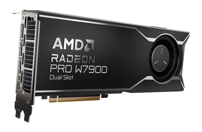
To say that the global foundry market is booming right now would be an understatement. Demand for leading-edge process technologies driven by AI and HPC applications is unprecedented, and with Intel joining the contract chipmaking game, this market segment is once again becoming rather competitive as well. Yet, this is exactly the market segment that Rapidus, a foundry startup backed by the Japanese government and several major Japanese companies, is going to enter in 2027, when its first fab comes online, just a few years from now.
In a fresh update on the status of bringing up the company's first leading-edge fab, Rapidus has revealed that they are intending to get in to the chip packaging game as well. Once complete, the ¥5 trillion ($32 billion) fab will be offering both chip lithography on a 2nm node, as well as packaging services for chips produced within the facility – a notable distinction in an industry where, even if packaging isn't outsourced entirely (OSAT), it's still normally handled at dedicated facilities.
Ultimately, while the company wants to serve the same clients as TSMC, Samsung, and Intel Foundry, the firm plans to do things almost completely differently than its competitors in a bid to speed up chipmaking from finishing design to getting a working chip out of the fab.
"We are very proud of being Japanese," said Henri Richard, general manager and president of Rapidus's subsidiary in the U.S. "[…] I know that some people may be looking at this thinking [that] Japan is known for quality, attention to detail, but not necessarily for speed, or flexibility. But I will tell you that Atsuyoshi Koike (the head of Rapidus) is a very special executive. That is, he has all the quality of Japan, with a lot of American thinking. So he is quite a unique guy, and certainly extraordinarily focused on creating a company that will be extremely flexible and extremely quick on its feet."
2nm Only, At First
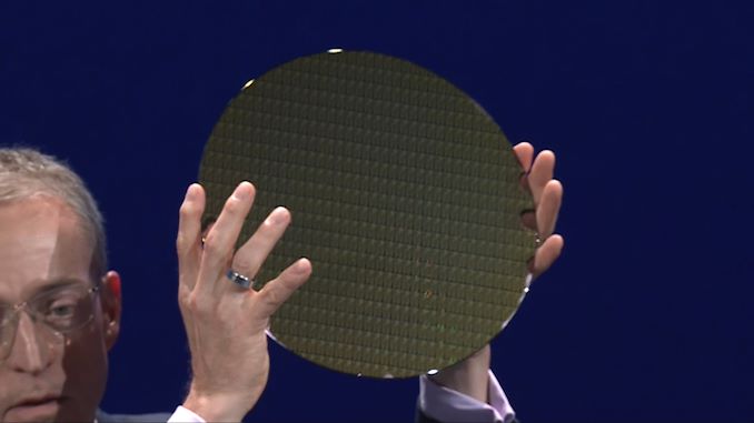
Perhaps the most significant difference between Rapidus and traditional foundries is that the company will offer only leading-edge manufacturing technologies to its clients: 2 nm in 2027 (phase 1) and then 1.4 nm in the future (phase 2). This is a stark contrast with other contract fabs, including Intel, which tend to offer their customers a full range of fabrication processes to land more clients and produce more chips. Apparently, Rapidus hopes that that there will be enough Japanese and American chip developers that are inclined to use its 2 nm fabrication process to produce their designs. With that said, the number of chip designers that are using the most advanced production node at any given time is relatively small – limited to large firms who need first-mover advantage and have the margins to justify taking the risk – so it remains to be seen whether Rapidus's business model becomes successful. The company believes it will, since the market of chips made on advanced nodes is growing rapidly.
"Until recently IDC was giving a an estimation of the 2nm and below market as about $80 billion and I think we are going to see soon a revision of the potential to $150 billion," said Richard. "[…] TSMC is the 800 pound gorilla in the space. Samsung is there and Intel is going to enter that space. But the market growth is so significant and the demand is so high, that it does not take a lot of market share for Rapidus to be successful. One of the things that gives me great comfort is that when I talk to our EDA partners, when I talk to our potential clients, it is obvious that the entire industry is looking for alternative supply from a fully independent foundry. There is a place for Samsung in this industry, there is a place for Intel in this industry, the industry is currently owned by TSMC. But another totally independent foundry is more than welcome by all of the ecosystem partners and by the customers. So, I feel really, really good about Rapidus's positioning."
Speaking of advanced process technologies, it is notable that Rapidus does not plan to use ASML's High-NA Twinscan EXE lithography scanners for 2 nm production. Instead, Rapidus is sticking to ASML's proven Low-NA scanners, which will reduce costs of Rapidus's fab, though it will entail usage of EUV double patterning, which brings up costs and lengthens the production cycle in other ways. Even with those trade-offs, SemiAnalysis analysts believe that given the cost of High-NA EUV litho tools and halved imaging field, Low-NA double patterning could be more economically viable.
"We think we are absolutely comfortable with the current [Low-NA EUV] solution for 2nm, but we might consider a different solution at 1.4 nm," said Richard.
For now, only Intel plans to use High-NA tools to make chips on its 14A (1.4 nm-class) fabrication process sometimes in the middle of the decade. TSMC and Samsung Foundry look to be more cautious, so Rapidus is not alone with its attitude towards High-NA EUV tools.
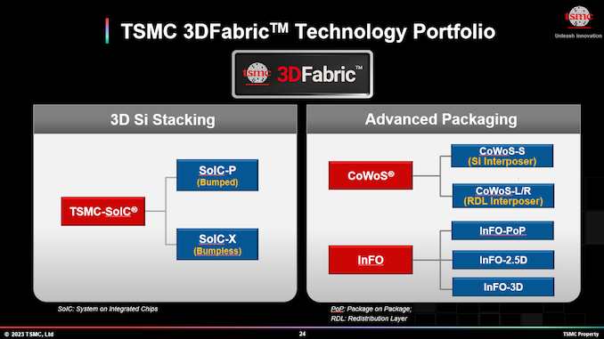
Advanced Packaging at a Leading-Edge Fab
In addition to advanced process technologies, high-end chip designers (such as those used for AI and HPC applications) also need advanced packaging technologies (e.g., for HBM integration) and Rapidus is ready to offer them as well. What sets the company apart from its industry peers is that it plans to build and package chips in the same fab.
"We intend to have the backend capability in Hokkaido [semiconductor fab] as a differentiator," Richard said. "We have the benefit of starting from scratch and be able to build probably the first fully integrated front end back end semiconductor fab in the industry, I think. Others will retrofit and modify their existing capacity, but we have a clean sheet of paper and part of the secret sauce that Koike son is bringing to Rapidus are some very interesting ideas on how to integrate both front end and back end amongst others."
Intel, Samsung, and TSMC have separate facilities for chip manufacturing and packaging, as even the most sophisticated packaging methods involving silicon interposers (which are essentially large chips) don't match the complexity of modern processors. The tools that are used to build silicon interposers and equipment used to make full logic chips are vastly different, so installing them into the same cleanroom generally makes little sense as they do not complement each other very well.
On the other hand, transporting wafers from one site to another is a time consuming and risky endeavor, so integrating everything into one campus could make sense as it greatly simplifies supply chain.
"We are going to re reinvent the way, chip design, front end and the back end are working together toward the completion of a project," Richard said. […] The whole idea is we can do it fast, with high quality, high yield, and with a very short cycle time."