Internships fabricate a microelectronics future
Nestled among the diverse labs and prototyping facilities at MIT Lincoln Laboratory, the Microelectronics Laboratory (ML) whirs away. Technicians in the ML fabricate advanced integrated circuits, which end up in systems that peer into the cosmos, observe weather from space, and power quantum computers — to name just a few uses. The ML is one of several facilities within Lincoln Laboratory’s Microsystems Prototyping Foundry (MPF) operations.
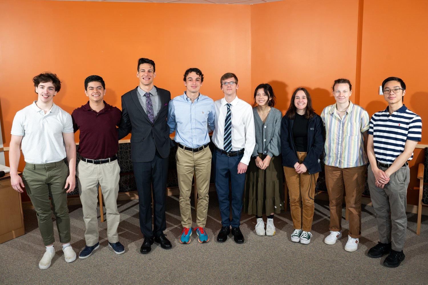
This summer, 12 students had a hand in MPF operations as part of the Massachusetts Microelectronics Internship Program. The Northeast Microelectronics Coalition started this program last year to help train the next generation of microelectronics professionals. Accepted undergraduates are placed in the region's leading microelectronics companies for 10 weeks. No prior experience is needed, only a willingness to learn.
Donning "bunny suits," the head-to-toe coverings staff wear to help keep the lab free from contaminants, the interns each conducted experiments to improve fabrication processes. The ML maintains an ultraclean certification, Class 10/ISO 4, meaning that the air contains a maximum of 10 particles (over 0.5 micron in size) per cubic foot. Even so, particles can still end up on the wafers — slices of semiconductor materials, like silicon, that form the base of circuits.
"Particles can be device killers. Cleanrooms control and reduce the amount and size of particles," says Peter Preston, an intern from Springfield Technical Community College (STCC). Over the summer, Preston assessed the number of particles present on wafers after they underwent specific processing steps and troubleshooted ways to lower that count. Fellow STCC student Travis Donelon sampled the ML's water supply to test for bacteria, which can introduce particles to the water during rinsing. He also analyzed the flow of nitrogen gas, an essential material for keeping surfaces free of moisture and particles throughout every step of the fabrication process.
In running these experiments, Preston and Donelon learned how to run each machine in the Compound Semiconductor Laboratory (CSL) within the MPF, training that could enable them to be “hired tomorrow as technicians," says Scott Eastwood, the CSL operations manager.
"Getting hands-on work with almost every tool used in the fabrication process was a great opportunity to see the big picture of what microelectronics is all about," Donelon says.
Dan Pulver, the ML group leader, says that the internships are helping the ML plot a route of growth. "We’re building skills and opportunity awareness, along with relationships, with more students who may go on to work in our group." A recent self-assessment showed that the ML has the most retirement risk of all groups at Lincoln Laboratory — a finding that mirrors the microelectronics workforce, both regionally and nationally.
Experts find that the industry's knowledge base is shrinking fast, as U.S. dominance in semiconductors has receded in recent decades. A chip shortage during the Covid-19 pandemic shone a light on the risks of relying on overseas microelectronics fabrication. The 2022 CHIPS (for Creating Helpful Incentives to Produce Semiconductors) and Science Act aims to ramp-up chip fabrication and innovation in the United States, but a new generation of workers will need the relevant knowledge to do so. This internship program was made possible, in part, by funding from CHIPS, which allocated $13.2 billion for R&D and workforce development.
Kara Stratton, a rising junior at Boston University, credits this internship with her decision to now pursue a nanotechnology concentration. Her summer project involved teasing out issues in the process of depositing platinum. In creating circuits, platinum (among other metals) is heated in a low-pressure chamber, vaporized, and deposited onto a wafer. She made changes to the platinum recipe and heat-up processes to reduce spitting, or uneven deposits.
"Having a hands-on job that taught me so much and gave me priceless experiences made me feel more confident in making the decision to pursue a career in microelectronics," Stratton says. "Lincoln Laboratory, and more specifically the ML, fosters an inclusive and innovative community of employees who were always willing to help me learn new things."
Some students will continue their work in the fall as student technical assistants. "We often see the eyes of students light up as they discuss new experiences and accomplishments — a great short-term reward. I think long term will work out, too," Pulver says. One student, Ian Pahl from Western New England University, hopes to progress his research in reducing ML energy use. One of his projects studied the impact of reducing airflow fan speeds, a change that could save the ML up to $100,000 a year along with carbon footprint reduction, according to Pulver.
Besides the time spent in the ML, each intern also gained mentorship, participated in training events, and learned more about the diverse projects undertaken at a federally funded R&D center. They received subsidized housing and transportation, as part of the many benefits Lincoln Laboratory offers through its wider Summer Research Program.
As Donelon heads back to school to study optics and photonics, he looks forward to expanding on his newfound knowledge. "My internship experience was nothing short of incredible. Coming from a switched major and community college, I was not expecting but very humbled to be working at such a prestigious laboratory. The work I have done over the summer has been both challenging and gratifying."
Students interested in applying for the Massachusetts Microelectronics Internship Program can learn more on the program’s website.

© Photo: Nicole Fandel

