FreshRSS

Normální zobrazení

Jsou dostupné nové články, klikněte pro obnovení stránky.
PředevčíremAnandTech
  • ✇AnandTech
  • The Eurocom 780W AC Power Adapter Review: Big Power For Big Laptops
    While desktop PC power supplies receive the bulk of enthusiasts’ attention for good reasons – not the least of which being the vast selection of options that comes from being a standardized part – power supplies as a whole aren’t just a concern for big PCs. With the majority of PC sales having flipped to notebook sales some years ago, notebook power supplies already lead the market in volume. And while most laptops don’t need the kind of massively powered PSUs that dominate the desktop space, ev
     

The Eurocom 780W AC Power Adapter Review: Big Power For Big Laptops

22. Duben 2024 v 15:00

While desktop PC power supplies receive the bulk of enthusiasts’ attention for good reasons – not the least of which being the vast selection of options that comes from being a standardized part – power supplies as a whole aren’t just a concern for big PCs. With the majority of PC sales having flipped to notebook sales some years ago, notebook power supplies already lead the market in volume. And while most laptops don’t need the kind of massively powered PSUs that dominate the desktop space, even that is slowly changing as desktop replacement-class laptops increasingly grow in performance and power consumption.

Perhaps the poster-child for the high-performance, high-powered laptop is Eurocom, who has a long history of developing heavy-duty DTR laptops that are all but portable desktop systems. Following recent trends in GPU power consumption and in GPU popularity for both gaming and AI workloads, the company has been selling a range of “mobile supercomputers”, which are practically large, tailor-made laptops that rival even the best of desktop computers – and have the power requirements to match.

In order to power their own high-end laptops, Eurocom has developed a rather unusual 780W AC adapter for high-performance laptops. Intended to power the most powerful of powerful laptops, their latest power adapter can supply over three-quarters of a kilowatt of DC power; a desktop-like wattage for a desktop-like device. It’s a laptop power adapter that’s unique in its scale, and with some room to scale up even further.

Eurocom 780W AC Adapter
Power specifications
RAIL +20V
MAX OUTPUT 39A
780W
DIMENSIONS 325 x 110 x 40mm, 1.38kg
AC INPUT 90 - 264 VAC, 50 - 60 Hz
MSRP PSU: $299, Cable: $129+

Eurocom has offered this adapter for a few years now. But it’s taken on a new life as more laptops have been released that use such a large adapter (or two smaller 300W-ish power adapters). And, critically, Eurocom has made additional DC cable/connector sets for other manufactuers’ laptops, significantly increasing the number of systems it’s compatible with. Currently, Eurocom offers DC cables for the following laptops:

  • Alienware M17x M18x; 1x DC Cable ; w/ barrel AW connector; 193cm/6.4ft 
  • Alienware AREA 51m; 1x DC Cable + Splitter Box w/ 2x barrel AW connectors; 152cm/5ft 
  • ASUS ROG G18 Strix; GX501V; GM501; GM501GM; GX531GM; 1x DC Cable; w/ barrel ROG connector 
  • ASUS G703GX, GZ700GX; 1x DC Cable w/ 2x ROG barrel connectors; 152cm/5ft 
  • CLEVO, OriginPC, Sager, XMG, EUROCOM laptops; 1x DC Cable; w/ 4-pin round connector; 182cm / 6ft 
  • CLEVO X370SNx; 1x DC Cable; w/ square connector; 120cm / 3.8ft 
  • CLEVO X170SM/X170KM; 1x DC Cable; w/ dual square connectors; 152cm / 5ft 
  • Dell Precision 7720/7710; 1x DC Cable; w/ barrel Dell connector; 120cm / 3.8ft 
  • MSI GE76, GT76, GT77, GE78HX Raider, Titan 18HX 1x DC Cable; w/ single square connector; 120cm / 3.8ft 
  • MSI laptops & MSI Trident AS Gaming Desktops; 1x DC Cable; w/ 4-pin round connector; 182cm / 6ft 

The Eurocom 780W AC Adapter

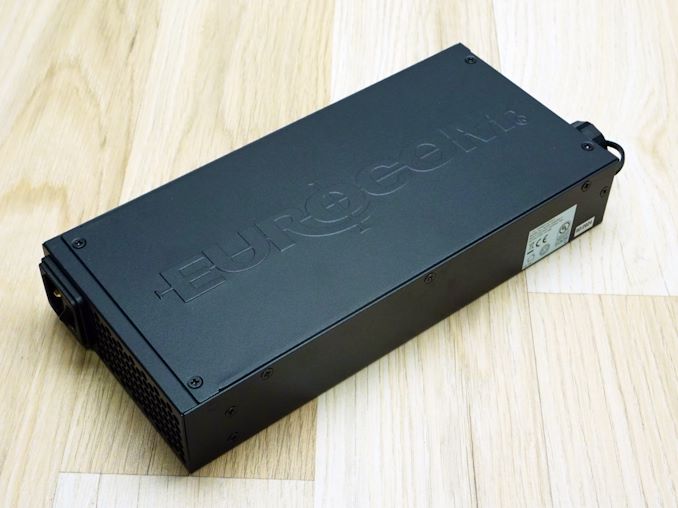
Externally, the Eurocom 780W AC adapter looks like a hybrid between a PC PSU and a laptop adapter. It is shaped like an oversized laptop AC adapter but has a metallic body and cooling vents/fans. Eurocom advertises that it weighs “only 1.34kg”, which is the weight of an entire 14-inch laptop by comparison, but is relatively lightweight for a PSU with that kind of power output. The company logo is debossed across the top side of the adapter, with four round anti-slip pads found at its bottom. Care needs to be taken while moving it around because the metallic edges and weight can spell trouble for wooden surfaces.

Eurocom installed a small information display on the AC adapter, which shows the current, voltage, and power output, as well as the temperature of the adapter. It is not perfectly accurate – we can see it was reading a 12W load without a DC cable attached to the adapter – but it works as a basic reference. Next to it, there is a heavy-duty metallic connector for the DC cable. On the other side we can find a typical three-prong C14 AC cable receptacle, as well as an on/off switch, which is not something commonly found on laptop AC adapters.


Opening up the chassis, we can see that the Eurocom 780W AC adapter is not unlike common PC PSUs – just less complex due to the need to only generate a single 20V rail. The basic layout is identical, with an AC filter at the input consisting of four Y capacitors, two X capacitors, and two substantial filtering inductors, that leads to a rectifying bridge. The GBJ1508 bridge is made by HY Electronic Cayman Ltd, a Taiwanese company we're encountering for the first time.


Then we have an APFC circuitry with a massive Aishi 450V/560μF capacitor and a large filtering coil being its passive components, with a Toshiba K31N60W regulator on the same heatsink as the two MOSFETs that form a typical half-bridge configuration. Following that we have a small transformer and two Infineon 045N10N MOSFETs to generate the 20V power output. Cooling is provided by two Protechnic Electric MGT3812XB-W20 38 mm fans, which are small but high quality products with a double-ball bearing engine.

Test Results (~25°C Ambient)

For the testing of PSUs, we are using high precision electronic loads with a maximum power draw of 2700 Watts, a Rigol DS5042M 40 MHz oscilloscope, an Extech 380803 power analyzer, two high precision UNI-T UT-325 digital thermometers, an Extech HD600 SPL meter, and various other bits and parts. 

The average efficiency of the Eurocom 780W AC adapter is very high, at 91.6% when the PSU is powered from an 230V AC source and drops down to 90.9% when powered from an 115V AC source. There is no 80Plus or similar efficiency certification covering this PSU, but there is legislation such as the Ecodesign 2019/1782 directive, and, even though the manufacturer does not fully publish its performance specs as the directive requires, the Eurocom 780W adapter seems to easily meet them. We must mention that this kind of PSU has an advantage over classic PC PSUs because it only generates a single voltage line, and conversion losses are lower, so it should not be directly compared to any multi-voltage output PSU.

The two small fans of the Eurocom 780W AC adapter seem hardwired to the power output of the unit, largely ignoring the temperature of the adapter and adjusting their speed only according to the load. Up to 40% load, which should cover the power needs of most gaming laptops anyway, the adapter is practically entirely silent. The speed of the fan gradually increases when the load is greater than 330 Watts, reaching terrifying noise figures at maximum load. Given the nature of the adapter, it is highly unlikely that it will operate at such high a load for prolonged periods of time, as even the laptops that require 2x330 Watt adapters will not continuously sustain such a high load.

Power Supply Quality 

The electrical performance of the Eurocom 780W AC adapter is surprisingly good compared to its datasheet specifications. Eurocom claims a maximum voltage ripple of 200 mV but we recorded a maximum of 116 mV, which is alright for a 20 V rail and better than we expected due to the mediocre secondary side filtering. Voltage regulation is very good, at just 1.2% across the nominal load range.

Main Output
Load (Watts) 158.03 394.68 586.46 780.78
Load (Percent) 20% Load 50% Load 75% Load 100% Load
  Amperes Volts Amperes Volts Amperes Volts Amperes Volts
20 V 7.8 20.26 19.5 20.24 29.25 20.05 39 20.02


Line Regulation
(20% to 100% load)
Voltage Ripple (mV)
20% Load 50% Load 75% Load 100% Load
20V 1.2% 44 66 82 116

During our routine evaluation, we examine the fundamental protection features of all power supply units we review, including Over Current Protection (OCP), Over Voltage Protection (OVP), Over Power Protection (OPP), and Short Circuit Protection (SCP). The Eurocom 780W AC adapter behaves quite oddly here, as it has a rated output of 39 A and a maximum output of 45 A for 25 ms. However, we were able to draw 50 A from the unit, which is nearly 1000 Watts, for several minutes without triggering the OCP/OPP protection. The PSU did not show any serious signs of stress or overheating over that time, nor poor electrical performance. The OPP protection triggers immediately once the load is greater than 50.3 A – and also immediately resets and restarts the PSU when the load drops below 50.2A. It would seem that this platform was initially designed to be significantly more powerful and the OEM “forgot” to adjust the OCP/OPP trigger points.

Conclusion

The Eurocom 780W AC adapter melds raw power with innovation, presenting a piece that's as formidable as it is intriguing. With its substantial weight and metallic edges, it demands respect and caution, especially on delicate surfaces. However, its weight is justified by the impressive power output it delivers, making it a powerhouse that somewhat overshadows its bulky, heavy-set design. The inclusion of a display for monitoring performance is a smart touch, though its accuracy leaves room for improvement.

On the inside, Eurocom doesn't skimp on quality. The adapter's internals are a testament to careful selection and engineering, closely mirroring the complexity and efficiency of high-end PC PSUs. Its cooling system, though compact, functions well and provides good performance without compromising on noise levels — at least under most loads. That said, the adapter's noise profile at maximum load might not be everyone's cup of tea, hinting at a balance yet to be perfected between power and tranquility.

Overall, Eurocom's 780W AC adapter boasts commendable efficiency and electrical performance. But as a premium-priced product – a complete unit and cable will set you back at least $429 – it could benefit from a touch more finesse, particularly in terms of user safety and operational noise at high loads. Otherwise, I'm personally a bit surprised that Eurocom isn't offering a open-ended cable for DIY enthusiasts, which could broaden its appeal and utility. Such an addition would not only cater to a wider audience but also underscore Eurocom's commitment to versatility and innovation.

In sum, while the adapter stands out for its power and performance, there's also a clear avenue for Eurocom to enhance its appeal through minor, yet impactful, improvements.

  • ✇AnandTech
  • JEDEC Extends DDR5 Memory Specification to 8800 MT/s, Adds Anti-Rowhammer Features
    When JEDEC released its DDR5 specification (JESD79) back in 2020, the standard setting organization defined precise specs for modules with speed bins of up to 6400 MT/s, while leaving the spec open to further expansions with faster memory as technology progressed. Now, a bit more than three-and-a-half years later, and the standards body and its members are gearing up to release a faster generation of DDR5 memory, which is being laid out in the newly updated JESD79-JC5 specification. The latest i
     

JEDEC Extends DDR5 Memory Specification to 8800 MT/s, Adds Anti-Rowhammer Features

22. Duben 2024 v 14:00

When JEDEC released its DDR5 specification (JESD79) back in 2020, the standard setting organization defined precise specs for modules with speed bins of up to 6400 MT/s, while leaving the spec open to further expansions with faster memory as technology progressed. Now, a bit more than three-and-a-half years later, and the standards body and its members are gearing up to release a faster generation of DDR5 memory, which is being laid out in the newly updated JESD79-JC5 specification. The latest iteration of the DDR5 spec defines official DDR timing specifications up to 8800 MT/s, as well as adding some new features when it comes to security.

Diving in, the new specification outlines settings for memory chips (on all types of memory modules) with data transfer rates up to 8800 MT/s (AKA DDR5-8800). This suggests that all members of the JESD79 committee that sets the specs for DDR5 — including memory chip makers and memory controller designers — agree that DDR5-8800 is a viable extension of the DDR5 specification both from performance and cost point of view. Meanwhile, the addition of higher speed bins is perhaps enabled by another JEDEC feature introduced in this latest specification, which is the Self-Refresh Exit Clock Sync for I/O training optimization.

JEDEC DDR5-A Specifications
AnandTech Data Rate
MT/s
CAS Latency (cycles) Absolute Latency (ns) Peak BW
GB/s
DDR5-3200 A 3200 22 22 22 13.75 25.6
DDR5-3600 A 3600 26 26 26 14.44 28.8
DDR5-4000 A 4000 28 28 28 14 32
DDR5-4400 A 4400 32 32 32 14.55 35.2
DDR5-4800 A 4800 34 34 34 14.17 38.4
DDR5-5200 A 5200 38 38 38 14.62 41.6
DDR5-5600 A 5600 40 40 40 14.29 44.8
DDR5-6000 A 6000 42 42 42 14 48
DDR5-6400 A 6400 46 46 46 14.38 51.2
DDR5-6800 A 6800 48 48 48 14.12 54.4
DDR5-7200 A 7200 52 52 52 14.44 57.6
DDR5-7600 A 7600 54 54 54 14.21 60.8
DDR5-8000 A 8000 56 56 56 14 64.0
DDR5-8400 A 8400 60 60 60 14.29 67.2
DDR5-8800 A 8800 62 62 62 14.09 70.4

When it comes to the JEDEC standard for DDR5-8800, it sets relatively loose timings of CL62 62-62 for A-grade devices and CL78 77-77 for lower-end C-grade ICs. Unfortunately, the laws of physics driving DRAM cells have not improved much over the last couple of years (or decades, for that matter), so memory chips still must operate with similar absolute latencies, driving up the relative CAS latency. In this case 14ns remains the gold standard, with CAS latencies at the new speeds being set to hold absolute latencies around that mark. But in exchange for systems willing to wait a bit longer (in terms of cycles) for a result, the new spec improves the standard's peak memory bandwidth by 37.5%.

This of course is just the timings set in the JEDEC specification, which is primarily of concern for server vendors. So we'll have to see just how much harder consumer memory manufacturers can push things for their XMP/EXPO-profiled memory. Extreme overclockers are already hitting speeds as high as 11,240 MT/s with current-generation DRAM chips and CPUs, so there may be some more headroom to play with in the next generation.

Meanwhile, on the security front, the updated spec makes a couple of changes that have been put in place seemingly to address rowhammer-style exploits. The big item here is Per-Row Activation Counting (PRAC), which true to its name, enables DDR5 to keep a count of how often a row has been activated. Using this information, memory controllers can then determine if a memory row has been excessively activated and is at risk of having its bits flipped, at which point they can back off to let the row properly refresh and the data re-stabilize.

Notably here, the JEDEC press release doesn't use the rowhammer name at any point (unfortunately, we haven't been able to see the specification itself). But based on the description alone, this is clearly intended to thwart rowhammer attacks, since these normally operate by forcing a bit flip between refreshes through a large number of activations.

Digging a bit deeper, PRAC seems to be based on a recent Intel patent, Perfect Row Hammer Tracking with Multiple Count Increments (US20220121398A1), which describes a very similar mechanism under the name "Perfect row hammer tracking" (PRHT). Notably, the Intel paper calls out that this technique has a performance cost associated with it because it increases the overall row cycle time. Ultimately, as the vulnerability underpinning rowhammer is a matter of physics (cell density) rather than logic, it's not too surprising to see that any mitigation of it comes with a cost.

The updated DDR5 specification also depreciates support for Partial Array Self Refresh (PASR) within the standard, citing security concerns. PASR is primarily aimed at power efficiency for mobile memory to begin with, and as a refresh-related technology, presumably overlaps some with rowhammer – be it a means to attack memory, or an obstruction to defending against rowhammer. Either way, with mobile devices increasingly moving to low-power optimized LPDDR technologies anyhow, the depreciation of PASR does not immediately look like a major concern for consumer devices.

  • ✇AnandTech
  • SK Hynix and TSMC Team Up for HBM4 Development
    SK hynix and TSMC announced early on Friday that they had signed a memorandum of understanding to collaborate on developing the next-generation HBM4 memory and advanced packaging technology. The initiative is designed to speed up the adoption of HBM4 memory and solidify SK hynix's and TSMC's leading positions in high-bandwidth memory and advanced processor applications. The primary focus of SK hynix's and TSMC's initial efforts will be to enhance the performance of the HBM4 stack's base die, wh
     

SK Hynix and TSMC Team Up for HBM4 Development

19. Duben 2024 v 17:00

SK hynix and TSMC announced early on Friday that they had signed a memorandum of understanding to collaborate on developing the next-generation HBM4 memory and advanced packaging technology. The initiative is designed to speed up the adoption of HBM4 memory and solidify SK hynix's and TSMC's leading positions in high-bandwidth memory and advanced processor applications.

The primary focus of SK hynix's and TSMC's initial efforts will be to enhance the performance of the HBM4 stack's base die, which (if we put it very simply) acts like an ultra-wide interface between memory devices and host processors. With HBM4, SK hynix plans to use one of TSMC's advanced logic process technologies to build base dies to pack additional features and I/O pins within the confines of existing spatial constraints. 

This collaborative approach also enables SK hynix to customize HBM solutions to satisfy diverse customer performance and energy efficiency requirements. SK hynix has been touting custom HBM solutions for a while, and teaming up with TSMC will undoubtedly help with this.

"TSMC and SK hynix have already established a strong partnership over the years. We've worked together in integrating the most advanced logic and state-of-the art HBM in providing the world's leading AI solutions," said Dr. Kevin Zhang, Senior Vice President of TSMC's Business Development and Overseas Operations Office, and Deputy Co-Chief Operating Officer. "Looking ahead to the next-generation HBM4, we're confident that we will continue to work closely in delivering the best-integrated solutions to unlock new AI innovations for our common customers."

Furthermore, the collaboration extends to optimizing the integration of SK hynix's HBM with TSMC's CoWoS advanced packaging technology. CoWoS is among the most popular specialized 2.5D packaging process technologies for integrating logic chips and stacked HBM into a unified module.

For now, it is expected that HBM4 memory will be integrated with logic processors using direct bonding. However, some of TSMC's customers might prefer to use an ultra-advanced version of CoWoS to integrate HBM4 with their processors.

"We expect a strong partnership with TSMC to help accelerate our efforts for open collaboration with our customers and develop the industry's best-performing HBM4," said Justin Kim, President and the Head of AI Infra at SK hynix. "With this cooperation in place, we will strengthen our market leadership as the total AI memory provider further by beefing up competitiveness in the space of the custom memory platform."

  • ✇AnandTech
  • AMD Announces Ryzen Pro 8000 and Ryzen Pro 8040 Series CPUs: Commercial Desktop Gets AI
    AMD is looking to drive the AI PC market with options across multiple product lines, which aren't limited to consumer processors. While primarily designed for the commercial sector, AMD has announced the Ryzen Pro 8000 'Phoenix' series of APUs for desktops, which AMD claims is the first professional-grade CPU to include an NPU designed to provide on-chip AI neural processing capabilities. AMD has also announced the Ryzen Pro 8040 'Hawk Point' series of mobile processors designed for commercial l
     

AMD Announces Ryzen Pro 8000 and Ryzen Pro 8040 Series CPUs: Commercial Desktop Gets AI

19. Duben 2024 v 16:00

AMD is looking to drive the AI PC market with options across multiple product lines, which aren't limited to consumer processors. While primarily designed for the commercial sector, AMD has announced the Ryzen Pro 8000 'Phoenix' series of APUs for desktops, which AMD claims is the first professional-grade CPU to include an NPU designed to provide on-chip AI neural processing capabilities. AMD has also announced the Ryzen Pro 8040 'Hawk Point' series of mobile processors designed for commercial laptops and notebooks.

AMD's Ryzen Pro 8000 and Ryzen Pro 8040 series processors come with support from AMD's Pro Manageability and AMD Pro Business Ready suites and are built with AMD's current generation Zen 4 cores. The Ryzen Pro 8000 and Ryzen Pro 8040 series processors are similar to their consumer-level counterparts. However, they have additional security features such as AMD Memory Guard, AMD Secure Processor, and Microsoft Pluton.

Touching on the differentiating factors between the non-Pro-consumer chips and the Ryzen Pro series, there is plenty for the commercial and enterprise market regarding security. In what is a first, the Ryzen Pro 8000 series is the first desktop platform to integrate Microsoft Pluton security features designed to protect when connecting to the cloud. Other features include AMD Memory Guard, which encrypts login credentials, keys, and text files stored in the DRAM. AMD Pro Security ties the AMD Zen 4 shadow stack and other layers in directly with the software stack, which, in this case, is Microsoft Windows 11 OS security. 

Another notable feature that AMD is hammering home is the on-chip AI capabilities of the included Ryzen AI neural processor unit (NPU), which allows enterprises to run AI workloads locally to mitigate privacy concerns by transferring data to and from the cloud. Although the current generation of NPUs embedded into processors are limited in what they can do, Ryzen AI is a driving factor within the AI PC, as manufacturers and SDVs are looking to utilize AI-accelerated features built into software, such as Microsoft with their AI-powered Copilot tool.

Although there are requirements that now must be met to ensure a PC is considered an 'AI PC,' Microsoft announced that their AI PC requirement is 45 TOPS of performance from the NPU alone, which none of the current generation of chips from AMD and Intel currently meet. In the desktop space, AMD currently has the lead as Intel has presently no offerings with an NPU, although, in the mobile space, AMD with their Ryzen 8040 (Hawk Point) and Intel with their Meteor Lake processors provide plenty of choice for users.

AMD Ryzen Pro 8000 Series (Zen 4)
AnandTech Cores
Threads
Base
Freq
Boost
Freq
L3
Cache
iGPU
 
TDP
Ryzen 7 Pro 8700G 8C / 16T 4200 5100 16 MB R780M (12 CUs) 45-65 W
Ryzen 7 Pro 8700GE 8C / 16T 3650 5100 16 MB R780M (12 CUs) 35 W
Ryzen 5 Pro 8600G 6C / 12T 4350 5000 16 MB R760M (8 CUs) 45-65 W
Ryzen 5 Pro 8500G 6C / 12T 3550 5000 16 MB R740M (4 CUs) 45-65 W
Ryzen 5 Pro 8600GE 6C / 12T 3900 5000 16 MB R760M (8 CUs) 35 W
Ryzen 5 Pro 8500GE 6C / 12T 3400 5000 16 MB R740M (4 CUs) 35 W
Ryzen 3 Pro 8300G 4C / 8T 3450 4900 8 MB R740M (4 CUs) 45-65 W
Ryzen 3 Pro 8300GE 4C / 8T 3500 4900 8 MB R740M (4 CUs) 35 W

Looking at the AMD Ryzen Pro 8000 series, AMD has announced eight new processors that include the same specifications as the non-Pro Ryzen 8000G APU counterparts. Two primary types of Ryzen Pro 8000 processors are set to be available: four with a configurable TDP of between 45 and 65 W and four with a flat TDP of 35 W for lower-powered environments. Leading the line-up is the Ryzen 7 Pro 8700G, which is identical in core specifications to the Ryzen 7 8700G APU, and has an 8C/16T (Zen 4) configuration with a base frequency of 4.2 GHz and a boost frequency of up to 5.1 GHz.

Even the Ryzen 7 Pro 8700GE, which is the 35 W version, has a 5.1 GHz boost frequency, although it has a slower base clock of 3.65 GHz. Both models have 16 MB of L3 cache, including AMD's integrated Radeon 780M (12 CUs) mobile graphics. All of the eight Ryzen Pro 8000 series models range from 4C/8T offerings with 8 MB of L3 cache and 4.9 GHz boost clocks, 6C/12T models with 5.0 GHz boost clocks and 16 MB of L3 cache, and those as mentioned above 8700/8700GE with 8C/16T.

While we take all performance figures given by manufacturers and vendors with a pinch of salt, AMD claims their Ryzen Pro 8000 series offers up to 19% better performance than Intel's 14th-gen Core series processors. AMD's match-up is the Ryzen 7 Pro 8700G vs. the Intel Core i7-14700, with AMD claiming a 47% victory in the Passmark 11 benchmark and 3X the graphics performance in 3D Mark Time Spy. This isn't entirely surprising because the Ryzen 7 Pro 8700G benefits from integrated RDNA3 graphics and AMD's Zen 4 cores.

AMD Ryzen Pro 8040 Series (Zen 4)
AnandTech Cores
Threads
Base
Freq
Boost
Freq
L3
Cache
iGPU TDP
Ryzen 9 Pro 8945HS 8C / 16T 4000 5200 16 MB 12 35-54 W
Ryzen 7 Pro 8845HS 8C / 16T 3800 5100 16 MB 12 35-54 W
Ryzen 7 Pro 8840HS 8C / 16T 3300 5100 16 MB 12 20-28 W
Ryzen 5 Pro 8645HS 6C / 12T 4300 5000 16 MB 8 35-54 W
Ryzen 5 Pro 8640HS 6C / 12T 3500 4900 16 MB 8 20-28 W
 
Ryzen 7 Pro 8840U 8C / 16T 3300 5100 16 MB 12 15-28 W
Ryzen 5 Pro 8640U 6C / 12T 3500 4900 16 MB 8 15-28 W
Ryzen 5 Pro 8540U* 6C / 12T 3200 4900 16 MB 4 15-28 W
*Ryzen 5 Pro 8540U is the only chip without AMD's Ryzen AI NPU

Moving onto AMD's latest Ryzen Pro 8040 processors for the mobile market, AMD has refreshed their Hawk Point family for the enterprise market. AMD has eight new processors, which are segmented into two families, the HS series and the U series. The HS series has five new chips, which range from 6C/12T up to 8C/16T, all with varying levels of clock speed and TDPs. At the top of the line-up is the Ryzen 9 Pro 8945HS, which is a direct replacement for the Ryzen 9 Pro 7940HS, and as such, it comes with the same 4.0 GHz base clock and 5.2 GHz boost clocks.

Pivitong to TDP, AMD offers the Ryzen 9 Pro 8945HS, Ryzen 7 Pro 8845HS, and Ryzen 5 Pro 8645HS with a configurable TDP of between 35 and 54 W. In contrast, the Ryzen 7 Pro 8840HS and the Ryzen 5 Pro 8640HS are designed for lower-powered laptops with a cTDP of 20-28 W. Regarding cache, all of the announced Ryzen Pro 8040 series models come with 16 MB of L3 Cache. At the same time, specifications such as the integrated graphics and clock speeds all correspond to the consumer line-up, the Ryzen 8040 series.

AMD's in-house performance figures show the Ryzen 7 Pro 8840U at 15 W performing better than Intel's Core Ultra 7 165H at 28 W. Still, as we always do with performance figures provided by vendors, take these with a pinch of salt. AMD claims a 30% combined increase in performance across the board in workloads, including Geekbench v6, Blender, PCMark 10, PCMark Night Raid, and UL Procyon. While there are plenty of different areas where performance gains and losses can be achieved, AMD does claim that their Ryzen 9 Pro 8945HS at 45 W vs. the Intel Core Ultra 9 185H at 45 W is 50% better in Topaz Labs Video AI Gaia 4X software; they did both use discrete graphics in this test according to AMD's slide deck.

The other notable thing is that all of the Ryzen Pro 8040 series processors, except the bottom SKU, the Ryzen 5 Pro 8540U, come with AMD's Ryzen AI NPU integrated into the silicon. While the AI PC ecosystem is still growing, AMD and over 150+ ISVs look to continue the trend that AI will power more software features in the future than we've seen so far. We are still in the infancy stage of the ecosystem despite much of the marketing targeting the AI functionality, but as we see higher-performing NPUs coming in the next generation of chips, at least ones that can match Microsoft 45 NPU TOPS requirement to run Copilot locally, much of the benefit of the NPU is currently down to how much power can be saved.

The introduction of the Ryzen Pro 8000/8040 series completes AMD's commercial client platform, along with the readily available Ryzen Threadripper Pro 7000-WX series for commercial and professional workstations. What sets these AMD Ryzen Pro series processors apart from the consumer (non-Pro) variants is support for the AMD Pro Manageability toolkit, which includes features such as cloud-based remote manageability to enable off-site IT technicians the ability to access devices remotely, as well WPA3 SAE encryption, which provides client-to-cloud protection for enterprises over shared networks.

AMD has not announced when the Ryzen Pro 8000 series APUs or the Ryzen Pro 8040 mobile chips will be available for purchase. However, we expect a wide array of OEMs, such as HP and Lenovo, to be already in the process of readying solutions that should hit the market soon.

  • ✇AnandTech
  • TSMC Posts Q1'24 Results: 3nm Revenue Share Drops Steeply, but HPC Share Rises
    Taiwan Semiconductor Manufacturing Co. this week released its financial results for Q1 2024. Due to a rebound in demand for semiconductors, the company garned $18.87 billion in revenue for the quarter, which is up 12.9% year-over-year, but a decline of 3.8% quarter-over-quarter. The company says that in increase in demand for HPC processors (which includes processors for AI, PCs, and servers) drove its revenue rebound in Q1, but surprisingly, revenue share of TSMC's flagship N3 (3nm-class) proce
     

TSMC Posts Q1'24 Results: 3nm Revenue Share Drops Steeply, but HPC Share Rises

19. Duben 2024 v 14:00

Taiwan Semiconductor Manufacturing Co. this week released its financial results for Q1 2024. Due to a rebound in demand for semiconductors, the company garned $18.87 billion in revenue for the quarter, which is up 12.9% year-over-year, but a decline of 3.8% quarter-over-quarter. The company says that in increase in demand for HPC processors (which includes processors for AI, PCs, and servers) drove its revenue rebound in Q1, but surprisingly, revenue share of TSMC's flagship N3 (3nm-class) process technology declined steeply quarter-over-quarter.

"Our business in the first quarter was impacted by smartphone seasonality, partially offset by continued HPC-related demand," said Wendell Huang, senior VP and chief financial officer of TSMC. "Moving into second quarter 2024, we expect our business to be supported by strong demand for our industry-leading 3nm and 5nm technologies, partially offset by continued smartphone seasonality."

In the first quarter of 2024, N3 wafer sales accounted for 9% of the foundry's revenue, down from 15% in Q4 2023, and up from 6% in Q3 2023. In terms of dollars, TSMC's 3nm production brought in around $1.698 billion, which is lower than $2.943 billion in the previous quarter. Meanwhile, TSMC's other advanced process technologies increased their revenue share: N5 (5 nm-class) accounted for 37% (up from 35%), and N7 (7 nm-class) commanded 19% (up from 17%). Though both remained relatively flat in terms of revenue, at $6.981 billion and $3.585 billion, respectively.

Generally, advanced technology nodes (N7, N5, N3) generated 65% of TSMC's revenue (down 2% from Q4 2023), while the broader category of FinFET-based process technologies contributed 74% to the company's total wafer revenue (down 1% from the previous quarter).

TSMC itself attributes the steep decline of N3's contribution to seasonally lower demand for smartphones in the first quarter as compared to the fourth quarter, which may indeed be the case as demand for iPhones typically slowdowns in Q1. Along those lines, there have also been reports about a drop in demand for the latest iPhones in China.

But even if A17 Pro production volumes are down, Apple remains TSMC's lead customer for N3B, as the fab also produces their M3, M3 Pro, and M3 Max processors on the same node. These SoCs are larger in terms of die sizes and resulting costs, so their contribution to TSMC's revenue should be quite substantial.

"Moving on to revenue contribution by platform. HPC increased 3% quarter-over-quarter to account for 46% of our first quarter revenue," said Huang. "Smartphone decreased 16% to account for 38%. IoT increased 5% to account for 6%. Automotive remained flat and accounted for 6%, and DCE increased 33% to account for 2%."

Meanwhile, as demand for AI and HPC processors will continue to increase in the coming years, TSMC expects its HPC platform to keep increasing its share in its revenue going forward.

"We expect several AI processors to be the strongest driver of our HPC platform growth and the largest contributor in terms of our overall incremental revenue growth in the next several years," said C.C. Wei, chief executive of TSMC.

  • ✇AnandTech
  • ASML Patterns First Wafer Using High-NA EUV Tool, Ships Second High-NA Scanner
    This week ASML is making two very important announcements related to their progress with high numerical aperature extreme ultraviolet lithography (High-NA EUV). First up, the company's High-NA EUV prototype system at its fab in Veldhoven, the Netherlands, has printed the first 10nm patterns, which is a major milestone for ASML and their next-gen tools. Second, the company has also revealed that it's second High-NA EUV system is now out the door as well, and has been shipped to an unnamed custome
     

ASML Patterns First Wafer Using High-NA EUV Tool, Ships Second High-NA Scanner

18. Duben 2024 v 15:00

This week ASML is making two very important announcements related to their progress with high numerical aperature extreme ultraviolet lithography (High-NA EUV). First up, the company's High-NA EUV prototype system at its fab in Veldhoven, the Netherlands, has printed the first 10nm patterns, which is a major milestone for ASML and their next-gen tools. Second, the company has also revealed that it's second High-NA EUV system is now out the door as well, and has been shipped to an unnamed customer.

"Our High-NA EUV system in Veldhoven printed the first-ever 10 nanometer dense lines," a statement by ASML reads. "Imaging was done after optics, sensors and stages completed coarse calibration. Next up: bringing the system to full performance. And achieving the same results in the field."

Our High NA EUV system in Veldhoven printed the first-ever 10 nanometer dense lines. ✨ Imaging was done after optics, sensors and stages completed coarse calibration.

Next up: bringing the system to full performance. And achieving the same results in the field. ⚙️ pic.twitter.com/zcA5V0ScUf

— ASML (@ASMLcompany) April 17, 2024

Alongside the system shipped to Intel at the end of 2023, ASML has retained their own Twinscan EXE:5000 scanner at their Veldhoven, Netherlands, facility, which is what the company is using for further research and development into High-NA EUV. Using that machine, the company has been able to print dense lines spaced 10 nanometers apart, which is a major milestone in photolithography development. Previously, only small-scale, experimental lab machines have been able to achieve this kind of a resolution. Eventually, High-NA EUV tools will achieve a resolution of 8 nm, which will be instrumental to build logic chips on technologies beyond 3 nm.

Intel's Twinscan EXE:5000 scanner at its D1X fab near Hillsboro, Oregon is also close behind, and its assembly is said to be nearing completion. That machine will be primarily used for Intel's own High-NA EUV R&D, with Intel slated to use its successor — the commercial-grade Twinscan EXE:5200 — to produce its chips on its Intel 14A (1.4 nm-class) in mass quantities in 2026 – 2027.

But Intel will not be the only chipmaker that gets to experiment with a High-NA EUV scanner for very long. As revealed by ASML, the company recently started shipping another Twinscan EXE:5000 machine to yet another customer. The fab tool maker is not disclosing the client, but previously it has said that all of leading logic and memory producers are in the process of procuring High-NA tools for R&D purposes, so the list of 'suspects' is pretty short.

"Regarding High-NA, or 0.55 NA EUV, we shipped our first system to a customer and this system is currently under installation," said Christophe Fouquet, chief business officer of ASML, at the company's earnings conference call with analysts and investors. "We started to ship the second system this month and its installation is also about to start."

While Intel plans to adopt High-NA EUV tools ahead of the industry, other chipmakers seem to a bit more cautious and plan to rely on risky yet already known Low-NA EUV double patterning method for production a 3 nm and 2 nm. Still, regardless of the exact timing for a transition, all of the major fabs will be relying on High-NA EUV tools in due time. So all parties have an interest in how ASML's R&D turns out.

"The customer interest for our [High-NA] system lab is high as this system will help both our Logic and Memory customers prepare for High-NA insertion into their roadmaps," said Fouquet. "Relative to 0.33 NA, the 0.55 NA system provides finer resolution enabling an almost 3x increase in transistor density, at a similar productivity, in support of sub-2nm Logic and sub-10nm DRAM nodes."

Sources: ASML/X, ASML, Reuters

  • ✇AnandTech
  • Intel and Sandia National Labs Roll Out 1.15B Neuron “Hala Point” Neuromorphic Research System
    While neuromorphic computing remains under research for the time being, efforts into the field have continued to grow over the years, as have the capabilities of the specialty chips that have been developed for this research. Following those lines, this morning Intel and Sandia National Laboratories are celebrating the deployment of the Hala Point neuromorphic system, which the two believe is the highest capacity system in the world. With 1.15 billion neurons overall, Hala Point is the largest d
     

Intel and Sandia National Labs Roll Out 1.15B Neuron “Hala Point” Neuromorphic Research System

17. Duben 2024 v 17:00

While neuromorphic computing remains under research for the time being, efforts into the field have continued to grow over the years, as have the capabilities of the specialty chips that have been developed for this research. Following those lines, this morning Intel and Sandia National Laboratories are celebrating the deployment of the Hala Point neuromorphic system, which the two believe is the highest capacity system in the world. With 1.15 billion neurons overall, Hala Point is the largest deployment yet for Intel’s Loihi 2 neuromorphic chip, which was first announced at the tail-end of 2021.

The Hala Point system incorporates 1152 Loihi 2 processors, each of which is capable of simulating a million neurons. As noted back at the time of Loihi 2’s launch, these chips are actually rather small – just 31 mm2 per chip with 2.3 billion transistors each, as they’re built on the Intel 4 process (one of the only other Intel chips to do so, besides Meteor Lake). As a result, the complete system is similarly petite, taking up just 6 rack units of space (or as Sandia likes to compare it to, about the size of a microwave), with a power consumption of 2.6 kW. Now that it’s online, Hala Point has dethroned the SpiNNaker system as the largest disclosed neuromorphic system, offering admittedly just a slightly larger number of neurons at less than 3% of the power consumption of the 100 kW British system.


A Single Loihi 2 Chip (31 mm2)

Hala Point will be replacing an older Intel neuromorphic system at Sandia, Pohoiki Springs, which is based on Intel’s first-generation Loihi chips. By comparison, Hala Point offers ten-times as many neurons, and upwards of 12x the performance overall,

Both neuromorphic systems have been procured by Sandia in order to advance the national lab’s research into neuromorphic computing, a computing paradigm that behaves like a brain. The central thought (if you’ll excuse the pun) is that by mimicking the wetware writing this article, neuromorphic chips can be used to solve problems that conventional processors cannot solve today, and that they can do so more efficiently as well.

Sandia, for its part, has said that it will be using the system to look at large-scale neuromorphic computing, with work operating on a scale well beyond Pohoiki Springs. With Hala Point offering a simulated neuron count very roughly on the level of complexity of an owl brain, the lab believes that a larger-scale system will finally enable them to properly exploit the properties of neuromorphic computing to solve real problems in fields such as device physics, computer architecture, computer science and informatics, moving well beyond the simple demonstrations initially achieved at a smaller scale.

One new focus from the lab, which in turn has caught Intel’s attention, is the applicability of neuromorphic computing towards AI inference. Because the neural networks themselves behind the current wave of AI systems are attempting to emulate the human brain, in a sense, there is an obvious degree of synergy with the brain-mimicking neuromorphic chips, even if the algorithms differ in some key respects. Still, with energy efficiency being one of the major benefits of neuromorphic computing, it’s pushed Intel to look into the matter further – and even build a second, Hala Point-sized system of their own.

According to Intel, in their research on Hala Point, the system has reached efficiencies as high as 15 TOPS-per-Watt at 8-bit precision, albeit while using 10:1 sparsity, making it more than competitive with current-generation commercial chips. As an added bonus to that efficiency, the neuromorphic systems don’t require extensive data processing and batching in advance, which is normally necessary to make efficient use of the high density ALU arrays in GPUs and GPU-like processors.

Perhaps the most interesting use case of all, however, is the potential for being able to use neuromorphic computing to enable augmenting neural networks with additional data on the fly. The idea behind this being to avoid re-training, as current LLMs require, which is extremely costly due to the extensive computing resources required. In essence, this is taking another page from how brains operate, allowing for continuous learning and dataset augmentation.

But for the moment, at least, this remains a subject of academic study. Eventually, Intel and Sandia want systems like Hala Point to lead to the development of commercial systems – and presumably, at even larger scales. But to get there, researchers at Sandia and elsewhere will first need to use the current crop of systems to better refine their algorithms, as well as better figure out how to map larger workloads to this style of computing in order to prove their utility at larger scales.

  • ✇AnandTech
  • Samsung Unveils 10.7Gbps LPDDR5X Memory - The Fastest Yet
    Samsung today has announced that they have developed an even faster generation of LPDDR5X memory that is set to top out at LPDDR5X-10700 speeds. The updated memory is slated to offer 25% better performance and 30% greater capacity compared to existing mobile DRAM devices from the company. The new chips also appear to be tangibly faster than Micron's LPDDR5X memory and SK hynix's LPDDR5T chips. Samsung's forthcoming LPDDR5X devices feature a data transfer rate of 10.7 GT/s as well as maximum cap
     

Samsung Unveils 10.7Gbps LPDDR5X Memory - The Fastest Yet

17. Duben 2024 v 16:00

Samsung today has announced that they have developed an even faster generation of LPDDR5X memory that is set to top out at LPDDR5X-10700 speeds. The updated memory is slated to offer 25% better performance and 30% greater capacity compared to existing mobile DRAM devices from the company. The new chips also appear to be tangibly faster than Micron's LPDDR5X memory and SK hynix's LPDDR5T chips.

Samsung's forthcoming LPDDR5X devices feature a data transfer rate of 10.7 GT/s as well as maximum capacity per stack of 32 GB. This allows Samsung's clients to equip their latest smartphones or laptops with 32 GB of low-power memory using just one DRAM package, which greatly simplifies their designs. Samsung says that 32 GB of memory will be particularly beneficial for on-device AI applications.

Samsung is using its latest-generation 12nm-class DRAM process technology to make its LPDDR5X-10700 devices, which allows the company to achieve the smallest LPDDR device size in the industry, the memory maker said.

In terms of power efficiency, Samsung claims that they have integrated multiple new power-saving features into the new LPDDR5X devices. These include an optimized power variation system that adjusts energy consumption based on workload, and expanded intervals for low-power mode that extend the periods of energy saving. These innovations collectively enhance power efficiency by 25% compared to earlier versions, benefiting mobile platforms by extending battery life, the company said.

“As demand for low-power, high-performance memory increases, LPDDR DRAM is expected to expand its applications from mainly mobile to other areas that traditionally require higher performance and reliability such as PCs, accelerators, servers and automobiles,” said YongCheol Bae, Executive Vice President of Memory Product Planning of the Memory Business at Samsung Electronics. “Samsung will continue to innovate and deliver optimized products for the upcoming on-device AI era through close collaboration with customers.”

Samsung plans to initiate mass production of the 10.7 GT/s LPDDR5X DRAM in the second half of this year. This follows a series of compatibility tests with mobile application processors and device manufacturers to ensure seamless integration into future products.

  • ✇AnandTech
  • The Iceberg Thermal IceFLOE Oasis 360mm AIO Cooler Review: Affordable & Effective Cooling
    Iceberg Thermal Inc. is one of the newer players in the PC cooling market. The company was founded in 2019 by an experienced team of designers and engineers setting off on their own, aiming to deliver a wide range of PC cooling products to industrial and commercial users alike. They only have a handful of retails products currently available, with the vast majority of them being CPU air coolers, but they have just launched their first liquid cooler products, the IceFLOE Oasis series. In today’s
     

The Iceberg Thermal IceFLOE Oasis 360mm AIO Cooler Review: Affordable & Effective Cooling

17. Duben 2024 v 14:00

Iceberg Thermal Inc. is one of the newer players in the PC cooling market. The company was founded in 2019 by an experienced team of designers and engineers setting off on their own, aiming to deliver a wide range of PC cooling products to industrial and commercial users alike. They only have a handful of retails products currently available, with the vast majority of them being CPU air coolers, but they have just launched their first liquid cooler products, the IceFLOE Oasis series.

In today’s review, we are having a look at the IceFLOE Oasis 360mm AIO (All-In-One) CPU cooler, the larger of the company's two recently-released liquid coolers. The IceFLOE Oasis CPU cooler targets the high-performance PC cooling market with a sub-$100 price point, aiming to deliver the performance needed to effectively cool a power-hungry processor without being a drain on the wallet in the process. This cooler features a 360mm radiator for an ample heat dissipation area, as well as housing for three high-airflow 120 mm fans. The IceFLOE Oasis supports a wide range of Intel and AMD socket types, making it compatible with a broad spectrum of CPUs. Additionally, it offers advanced RGB lighting, allowing users to customize the aesthetic of their cooling system.

  • ✇AnandTech
  • Samsung To Receive $6.4 Billion Under CHIPS Act to Build $40 Billion Fab in Texas
    Samsung Electronics this week was awarded up to $6.4 billion from the U.S. government under the CHIPS and Science Act to build its new fab complex in Taylor, Texas. This is the third major award under the act in the last month, with all three leading-edge fabs – Intel, TSMC, and now Samsung – receiving multi-billion dollar funding packages under the domestic chip production program. Overall, the final price tag on Samsung's new fab complex is expected to reach $40 billion by the time it's comple
     

Samsung To Receive $6.4 Billion Under CHIPS Act to Build $40 Billion Fab in Texas

16. Duben 2024 v 23:00

Samsung Electronics this week was awarded up to $6.4 billion from the U.S. government under the CHIPS and Science Act to build its new fab complex in Taylor, Texas. This is the third major award under the act in the last month, with all three leading-edge fabs – Intel, TSMC, and now Samsung – receiving multi-billion dollar funding packages under the domestic chip production program. Overall, the final price tag on Samsung's new fab complex is expected to reach $40 billion by the time it's completed later this decade.

Samsung's CHIPS Act funding was announced during a celebratory event attended by U.S. Secretary of Commerce Gina Raimondo and Samsung Semiconductor chief executive Kye Hyun Kyung.  During the event, Kyung outlined the strategic goals of the expansion, emphasizing that the additional funding will not only increase production capacity but also strengthen the entire local semiconductor ecosystem. Samsung plans to equip its fab near Taylor, Texas, with the latest wafer fab tools to produce advanced chips. The Financial Times reports that Samsung aims to produce semiconductors on its 2nm-class process technology starting 2026, though for now this is unofficial information.

"I am pleased to announce a preliminary agreement between Samsung and the Department of Commerce to bring Samsung's advanced semiconductor manufacturing and research and development to Texas," said Joe Biden, the U.S. president, in a statement. "This announcement will unleash over $40 billion in investment from Samsung, and cement central Texas's role as a state-of-the-art semiconductor ecosystem, creating at least 21,500 jobs and leveraging up to $40 million in CHIPS funding to train and develop the local workforce. These facilities will support the production of some of the most powerful chips in the world, which are essential to advanced technologies like artificial intelligence and will bolster U.S. national security."

Samsung has been a significant contributor to the Texas economy for decades, starting chip manufacturing in the U.S. in 1996. With previous investments totaling $18 billion in its Austin operations, Samsung's expansion into Taylor with an additional investment of at least $17 billion underscores its role as one of the largest foreign direct investors in U.S. history. The total expected investment in the new fab surpasses $40 billion, making it one of the largest for a greenfield project in the nation and transforming Taylor into a major hub for semiconductor manufacturing.

The CEO highlighted the substantial economic impact of Samsung's operations, noting a nearly double increase in regional economic output from $13.6 billion to $26.8 billion between 2022 and 2023. The ongoing expansion is projected to further stimulate economic growth, create thousands of jobs, and enhance the community's overall development.

“We are not just expanding production facilities; we’re strengthening the local semiconductor ecosystem and positioning the U.S. as a global semiconductor manufacturing destination.” said Kyung. “To meet the expected surge in demand from U.S. customers, for future products like AI chips, our fabs will be equipped for cutting-edge process technologies and help bring security to the U.S. semiconductor supply chain.”

Samsung is also committed to environmental sustainability and workforce development. The company plans to operate using 100% clean energy and incorporate advanced water management technologies. Additionally, it is investing in education and training programs to develop a new generation of semiconductor professionals. These initiatives include partnerships with educational institutions and programs tailored for military veterans.

In his remarks, Kyung expressed gratitude to President Biden, Secretary Raimondo, and other governmental and community supporters for their ongoing support. This collaborative effort between Samsung and various levels of government, as well as the local community, is pivotal in advancing America's semiconductor industry and ensuring its global competitiveness.

"Today’s announcement will help Samsung bring more semiconductor production, innovation, and jobs to U.S. shores, reinforcing America’s economy, competitiveness, and critical chip supply chains," a statememt by the Semiconductor Industry Associate reads. "We applaud Samsung for investing boldly in U.S.-based manufacturing and salute the U.S. Commerce Department for making significant headway in implementing the CHIPS Act’s manufacturing incentives and R&D programs. We look forward to continuing to work with leaders in government and industry to ensure the CHIPS Act remains on track to help reinvigorate U.S. chip manufacturing and research for many years to come."

  • ✇AnandTech
  • NVIDIA Intros RTX A1000 and A400: Entry-Level ProViz Cards Get Ray Tracing
    With NVIDIA’s Turing architecture turning six years old this year, the company has been retiring many of the remaining Turing products from its video card lineup. And today that spirit of spring cleaning is coming to the entry-level segment of NVIDIA’s professional visualization lineup, where NVIDIA is introducing a pair of new desktop cards based on their low-end Ampere hardware. The new RTX A1000 and RTX A400 cards will be replacing the T1000/T600/T400 lineup, which was released three years a
     

NVIDIA Intros RTX A1000 and A400: Entry-Level ProViz Cards Get Ray Tracing

16. Duben 2024 v 18:00

With NVIDIA’s Turing architecture turning six years old this year, the company has been retiring many of the remaining Turing products from its video card lineup. And today that spirit of spring cleaning is coming to the entry-level segment of NVIDIA’s professional visualization lineup, where NVIDIA is introducing a pair of new desktop cards based on their low-end Ampere hardware.

The new RTX A1000 and RTX A400 cards will be replacing the T1000/T600/T400 lineup, which was released three years ago in 2021. The new cards slot into the same entry-level category and finally finish fleshing out the RTX A series of proviz cards, offering NVIDIA’s Ampere-generation professional graphics technologies in the lowest-power, lowest-performance, lowest-cost configuration possible.

Notably, since the entry-level T-series were based on NVIDIA’s feature-limited TU11x silicon, which lacked ray tracing and tensor core support – the basis of NVIDIA’s RTX technologies and associated branding – this marks the first time these technologies will be available in NVIDIA’s entry-level desktop proviz cards. And accordingly, these are being promoted to RTX-branded video cards, ending the odd overlap with NVIDIA’s compute cards, which never carry RTX branding.

It goes without saying that as low-end cards, the ray tracing performance of either part is nothing to write home about, but it gives NVIDIA’s current proviz lineup a consistent set of graphics features from top to bottom.

NVIDIA Professional Visualization Card Specification Comparison
  A1000 A400 T1000 T400
CUDA Cores 2304 768 896 384
Tensor Cores 72 24 N/A N/A
Boost Clock 1460MHz 1755MHz 1395MHz 1425MHz
Memory Clock 12Gbps GDDR6 12Gbps GDDR6 10Gbps GDDR6 10Gbps
GDDR6
Memory Bus Width 128-bit 64-bit 128-bit 64-bit
VRAM 8GB 4GB 8GB 4GB
Single Precision 6.74 TFLOPS 2.7 TFLOPS 2.5 TFLOPS 1.09 TFLOPS
Tensor Performance 53.8 TFLOPS 21.7 TFLOPS N/A N/A
TDP 50W 50W 50W 30W
Cooling Active, SS Active, SS Active, SS Active, SS
Outputs 4x mDP 1.4a 4x mDP 1.4a 3x mDP 1.4a
GPU GA107 TU117
Architecture Ampere Turing
Manufacturing Process Samsung 8nm TSMC 12nm
Launch Date 04/2024 05/2024 05/2021 05/2021

Both the A1000 and A400 are based on the same board design, with NVIDIA doing away with any pretense of physical feature differentiation this time around (T400 was missing its 4th Mini DisplayPort). This means both cards are based on the GA107 GPU, sporting different core and memory configurations.

RTX A1000 is a not-quite-complete configuration of GA107, with 2304 CUDA cores and 72 tensor cores. This is paired with 8GB of GDDR6, which runs at 12Gbps, for a total of 192GB/second of memory bandwidth. The TDP of the card is 50 Watts, matching its predecessor.

Meanwhile RTX A400 is far more cut down, offering about a third of the active hardware on the GPU itself, and half the memory bandwidth. On paper this gives it around 40% of T1000’s performance, and half the memory bandwidth – or 96GB/second. Notably, despite the hardware cut-down, the official TDP is still 50 Watts, versus the 30 Watts of its predecessor. So at this point NVIDIA will soon cease offering a desktop proviz card lower than 50 Watts.

As noted before, both cards otherwise feature the same physical design, with a half-height half-length (HHHL) board with active cooling. As you’d expect from such low-TDP cards, these are single-slot cooler designs. Both cards feature a quartet of Mini DisplayPorts, with the same DP 1.4a functionality that we’ve seen across all of NVIDIA’s products for the last several years.

Finally, video-focused users will want to make note that the A1000/A400 have slightly different video capabilities. While A1000 gets access to both of GA107’s NVDEC video decode blocks, A400 only gets access to a single block – one more cutback to differentiate the two cards. Otherwise, both video cards get access to the GPU’s sole NVENC block.

According to NVIDIA, the RTX A1000 will be available starting today through its distribution partners. Meanwhile the RTX A400 will hit distribution channels in May, and with OEMs expected to begin offering the cards as part of their pre-built systems this summer.

  • ✇AnandTech
  • SK hynix Tube T31 Stick SSD Review: Bridging Solution Springs A Surprise
    SK hynix is one of the few vertically integrated manufacturers in the flash-based storage market. The company is well-established in the OEM market. A few years back, they also started exploring direct end-user products. Internal SSDs (starting with the Gold S31 and Gold P31) were the first out of the door. Late last year, the company introduced the Beetle X31 portable SSD, its first direct-attached storage product. In February, a complementary product was introduced - the Tube T31 Stick SSD. T
     

SK hynix Tube T31 Stick SSD Review: Bridging Solution Springs A Surprise

15. Duben 2024 v 14:00

SK hynix is one of the few vertically integrated manufacturers in the flash-based storage market. The company is well-established in the OEM market. A few years back, they also started exploring direct end-user products. Internal SSDs (starting with the Gold S31 and Gold P31) were the first out of the door. Late last year, the company introduced the Beetle X31 portable SSD, its first direct-attached storage product. In February, a complementary product was introduced - the Tube T31 Stick SSD.

The Beetle X31 is a portable SSD with a Type-C upstream port and a separate cable. The Tube T31 is a take on the traditional thumb drive with a male Type-A interface. The size of the Beetle X31 makes the use of a bridge solution obvious. Our investigation into the Tube T31 also revealed the use of the same internal SSD, albeit with a different bridge. Read on for a detailed look at the Tube T31, including an analysis of its internals and evaluation of its performance consistency, power consumption, and thermal profile.

  • ✇AnandTech
  • Corsair Enters Workstation Memory Market with WS Series XMP/EXPO DDR5 RDIMMs
    Corsair has introduced a family of registered memory modules with ECC that are designed for AMD's Ryzen Threadripper 7000 and Intel's Xeon W-2400/3400-series processors. The new Corsair WS DDR5 RDIMMs with AMD EXPO and Intel XMP 3.0 profiles will be available in kits of up to 256 GB capacity and at speeds of up to 6400 MT/s. Corsair's family of WS DDR5 RDIMMs includes 16 GB modules operating at up to 6400 MT/s with CL32 latency as well as 32 GB modules functioning at 5600 MT/s with CL40 latency
     

Corsair Enters Workstation Memory Market with WS Series XMP/EXPO DDR5 RDIMMs

12. Duben 2024 v 14:30

Corsair has introduced a family of registered memory modules with ECC that are designed for AMD's Ryzen Threadripper 7000 and Intel's Xeon W-2400/3400-series processors. The new Corsair WS DDR5 RDIMMs with AMD EXPO and Intel XMP 3.0 profiles will be available in kits of up to 256 GB capacity and at speeds of up to 6400 MT/s.

Corsair's family of WS DDR5 RDIMMs includes 16 GB modules operating at up to 6400 MT/s with CL32 latency as well as 32 GB modules functioning at 5600 MT/s with CL40 latency. At present, Corsair offers a quad-channel 64 GB kit (4×16GB, up to 6400 MT/s), a quad-channel 128GB kit (4×32GB, 5600 MT/s), an eight-channel 128 GB kit (8×16GB, 5600 MT/s), and an eight-channel 256 GB kit (8×32GB, 5600 MT/s) and it remains to be seen whether the company will expand the lineup.

Corsair's WS DDR5 RDIMMs are designed for AMD's TRX50 and WRX90 platforms as well as Intel's W790 platform and are therefore compatible with AMD's Ryzen Threadripper Pro 7000 and 7000WX-series as well as Intel's Xeon W-2400/3400-series CPUs. The modules feature both AMD EXPO and Intel XMP 3.0 profiles to easily set their beyond-JEDEC-spec settings and come with thin heat spreaders made of pyrolytic graphite sheet (PGS), which thermal conductivity than that of copper and aluminum of the same thickness. For now, Corsair does not disclose which RCD and memory chips its registered memory modules use.

Unlike many of its rivals among leading DIMM manufacturers, Corsair did not introduce its enthusiast-grade RDIMMs when AMD and Intel released their Ryzen Threadripper and Xeon W-series platforms for extreme workstations last year. It is hard to tell what the reason for that is, but perhaps the company wanted to gain experience working with modules featuring registered clock drivers (RCDs) as well as AMD's and Intel's platforms for extreme workstations.

The result of the delay looks to be quite rewarding: unlike modules from its competitors that either feature AMD EXPO or Intel XMP 3.0 profiles, Corsair's WS DDR5 RDIMMs come with both. While this may not be important on the DIY market where people know exactly what they are buying for their platform, this is a great feature for system integrators, which can use Corsair WS DDR5 RDIMMs both for their AMD Ryzen Threadripper and Intel Xeon W-series builds, something that greatly simplifies their inventory management.

Since Corsair's WS DDR5 RDIMMs are aimed at workstations and are tested to offer reliable performance beyond JEDEC specifications, they are quite expensive. The cheapest 64 GB DDR5-5600 CL40 kit costs $450, the fastest 64 GB DDR5-6400 CL32 kit is priced at $460, whereas the highest end 256 GB DDR5-5600 CL40 kit is priced at $1,290.

  • ✇AnandTech
  • Western Digital Previews 4 TB SD Card: World's Highest-Capacity
    Western Digital this week is previewing the industry's first 4 TB SD card. The device is being showcased at the NAB trade show for broadcasters and content creators and will be released commercially in 2025. Western Digital's SanDisk Extreme Pro SDUC 4 TB SD card complies with the Secure Digital Ultra Capacity standard (SDUC, which enables up to 128TB). The card uses the Ultra High Speed-I (UHS-I) interface and is rated for speed Class 10, therefore supporting a minimum speed of 10 MB/s and a m
     

Western Digital Previews 4 TB SD Card: World's Highest-Capacity

12. Duben 2024 v 00:30

Western Digital this week is previewing the industry's first 4 TB SD card. The device is being showcased at the NAB trade show for broadcasters and content creators and will be released commercially in 2025.

Western Digital's SanDisk Extreme Pro SDUC 4 TB SD card complies with the Secure Digital Ultra Capacity standard (SDUC, which enables up to 128TB). The card uses the Ultra High Speed-I (UHS-I) interface and is rated for speed Class 10, therefore supporting a minimum speed of 10 MB/s and a maximum data transfer rate of 104 MB/s when working in UHS104 (SDR104) mode (there is a catch about performance, but more on that later). WD's SD card is also rated to meet Video Speed Class V30, supporting a minimal sequential write speed of 30 MB/s, which is believed to be good enough for 8K video recording, above and beyond the 4K video market that Western Digital is primarily aiming the forthcoming card at.

For now, Western Digital is not disclosing what NAND is in the SanDisk Extreme Pro SDUC 4 TB SD card. Given the high capacity and relatively distant 2025 release date, WD may be targetting this as one of their first products to use their forthcoming BiCS 9 NAND.

And while not listed in WD's official press release, we would be surprised if the forthcoming card didn't also support the off-spec DDR200/DDR208 mode, which allows for higher transfer rates than the UHS-I standard normally allows via double data rate signaling. Western Digital's current-generation SanDisk Extreme Pro SDXC 1 TB SD card already supports that mode, allowing it to reach read speeds as high as 170 MB/s, so it would be surprising to see the company drop it from newer products. That said, the catch with DDR208 remains the same as always: it's a proprietary mode that requires a compatible host to make use of.

Western Digital has not disclosed how much will its SanDisk Extreme Pro SDUC 4 TB SD card cost. A 1 TB SanDisk Extreme Pro card costs $140, so one can make guesses about the price of a 4 TB SD card that uses cutting-edge NAND.

  • ✇AnandTech
  • AMD Quietly Launches Ryzen 7 8700F and Ryzen 5 8400F Processors
    AMD has recently expanded its Ryzen 8000 series by introducing the Ryzen 7 8700F and Ryzen 5 8400F processors. Initially launched in China, these chips were added to AMD's global website, signaling they are available worldwide, apparently from April 1st. Built from the recent Zen 4-based Phoenix APUs using the TSMC 4nm node as their Zen 4 mobile chips, these new CPUs lack integrated graphics. However, the Ryzen 7 8700F does include the integrated Ryzen AI NPU for added capabilities in a world cu
     

AMD Quietly Launches Ryzen 7 8700F and Ryzen 5 8400F Processors

11. Duben 2024 v 21:30

AMD has recently expanded its Ryzen 8000 series by introducing the Ryzen 7 8700F and Ryzen 5 8400F processors. Initially launched in China, these chips were added to AMD's global website, signaling they are available worldwide, apparently from April 1st. Built from the recent Zen 4-based Phoenix APUs using the TSMC 4nm node as their Zen 4 mobile chips, these new CPUs lack integrated graphics. However, the Ryzen 7 8700F does include the integrated Ryzen AI NPU for added capabilities in a world currently dominated by AI and moving it directly into the PC.

The company's decision to announce these chips in China aligns with its strategy to offer Ryzen solutions at every price point in the market. Although AMD didn't initially disclose the full specifications of these F-series models, and we did reach out to the company to ask about them, they refused to discuss them with us. Their listing on the website has now been updated with a complete list of specifications and features, with everything but the price mentioned.

AMD Ryzen 8000G vs. Ryzen 8000F Series (Desktop)
Zen 4 (Phoenix)
AnandTech Cores/Threads Base
Freq
Turbo
Freq
GPU GPU
Freq
Ryzen AI
(NPU)
L3 Cache
(MB)
TDP MSRP
Ryzen 7
Ryzen 7 8700G 8/16 4200 5100 R780M
12 CUs
2900 Y 16 65W $329
Ryzen 7 8700F 8/16 4100 5000 - - Y 16 65W ?
Ryzen 5
Ryzen 5 8600G 6/12 4300 5000 R760M
8 CUs
2800 Y 16 65W $229
Ryzen 5 8400F 6/12 4200 4700 - - N 16 65W ?

The Ryzen 7 8700F features an 8C/16T design, with 16MB of L3 cache and the same 65W TDP as the Ryzen 7 8700G. Although the base clock speed is 4.1 GHz, it boosts to 5.0 GHz; this is 100 MHz less on both base/boost clocks than the 8700G. Meanwhile, the Ryzen 5 8400F is a slightly scaled-down version of the Ryzen 8600G APU, with 6C/12, 16MB of L3 cache, and again has a 100 MHz reduction to base clocks compared to the 8600G. Unlike the Ryzen 5 8400F, the Ryzen 7 8700F keeps AMD's Ryzen AI NPU, adding additional capability for generative AI. 

The Ryzen 5 8400F can boost up to 4.7 GHz, 300 MHz slower than the Ryzen 5 8600G. AMD also allows overclocking for these new F-series chips, which means users could potentially boost the performance of these processors to match their G-series equivalents.

Pricing details are still pending, but to remain competitive, AMD will likely need to price these CPUs below the 8700G and 8600G, as well as the Ryzen 7 7700 and Ryzen 5 7600. These CPUs offer, albeit very limited, integrated graphics and have double the L3 cache capacity, along with higher boost clocks than the 8000F series chips, so pricing is something to consider whenever pricing becomes available.

  • ✇AnandTech
  • Intel Teases Lunar Lake At Intel Vision 2024: 100+ TOPS Overall, 45 TOPS From NPU Alone
    During the main keynote at Intel Vision 2024, Intel CEO Pat Gelsinger flashed a completed Lunar Lake chip off, much like EVP and General Manager of Intel's Client Computing Group (CCG) Michelle Johnston Holthaus did back at CES 2024. The contrast between the two glimpses of the Lunar Lake chip is that Pat Gelsinger gave us something juicier than just a photo op. He clarified and claimed the levels of AI performance we can expect to see when Lunar Lake launches. According to Intel's CEO Pat Gels
     

Intel Teases Lunar Lake At Intel Vision 2024: 100+ TOPS Overall, 45 TOPS From NPU Alone

11. Duben 2024 v 19:00

During the main keynote at Intel Vision 2024, Intel CEO Pat Gelsinger flashed a completed Lunar Lake chip off, much like EVP and General Manager of Intel's Client Computing Group (CCG) Michelle Johnston Holthaus did back at CES 2024. The contrast between the two glimpses of the Lunar Lake chip is that Pat Gelsinger gave us something juicier than just a photo op. He clarified and claimed the levels of AI performance we can expect to see when Lunar Lake launches.

According to Intel's CEO Pat Gelsinger, Lunar Lake, scheduled to be launched towards the end of this year, is set to raise the bar even further regarding on-chip AI capabilities and performance. At Intel's own Vision event, aptly named Intel Vision, current CEO of Intel Pat Gelsinger stated during his presentation that Lunar Lake will be the 'flagship SoC' for the next generation of AI PCs. Intel claims that Lunar Lake will have 3X the AI performance of their current Meteor Lake SoC, which is impressive as Meteor Lake is estimated to be running around 34 TOPS combined with the NPU, GPU, and CPU.

Factoring in the NPU within Meteor Lake, 11 of the 34 TOPS come solely from the NPU. Still, Intel claims that the NPU on Lunar Lake will hit a large 45 TOPs, akin to the Hailo-10 add-in card and similar to Qualcomm's Snapdragon X Elite processor. Factoring in the integrated graphics and the compute cores, Intel is claiming a combined total of over 100 TOPS, and with Microsoft's self-imposed guidelines of what constitutes an 'AI PC' coming in at 40 TOPS, Intel's NPU fits the bill.

Intel also alludes to how they are gaining a load of TOPS performance from the NPU, whether that be with new technologies; the NPU will likely be built in a more advanced node, perhaps Intel 18A. Another thing Intel didn't highlight was how they were measuring the TOPS performance, whether that be INT8 or INT4.

Still, one thing is clear: Intel wants to increase on-chip AI capabilities in desktop PCs and notebooks with each generation. Intel is also attempting to leverage more AI performance to help boost its goal to ship 100 million AI PCs by the end of 2025. Intel has already announced that it's shipped 5 million thus far and plans to sell another 40 million units by the end of the year.

  • ✇AnandTech
  • The Intel Core Ultra 7 155H Review: Meteor Lake Marks A Fresh Start To Mobile CPUs
    One of the most significant talking points of the last six months in mobile computing has been Intel and their disaggregated Meteor Lake SoC architecture. Meteor Lake, along with the new Core and Core Ultra naming scheme, also heralds the dawn of their first tiled architecture for the mobile landscape on the latest Intel 4 node with Foveros packaging. In December last year, Intel unveiled their premier Meteor lake-based Core Ultra H series, with five SKUs ranging from two with 4P+8E+2LP/18T and
     

The Intel Core Ultra 7 155H Review: Meteor Lake Marks A Fresh Start To Mobile CPUs

11. Duben 2024 v 14:30

One of the most significant talking points of the last six months in mobile computing has been Intel and their disaggregated Meteor Lake SoC architecture. Meteor Lake, along with the new Core and Core Ultra naming scheme, also heralds the dawn of their first tiled architecture for the mobile landscape on the latest Intel 4 node with Foveros packaging. In December last year, Intel unveiled their premier Meteor lake-based Core Ultra H series, with five SKUs ranging from two with 4P+8E+2LP/18T and three with 6P+8E+2LP/22T models. Since then, many vendors and manufacturers have launched notebooks capitalizing on Intel's latest multi-tiled Meteor Lake SoC architecture as the heart of power and performance, driving their latest models into 2024.

Today, we will focus on an attractive ultrabook via the ASUS Zenbook 14 OLED (UX3405MA), which features a thin and light design and is powered by Intel's latest Meteor Lake Core Ultra 7 155H processor. While much of the attention is going to come on how the Intel Core Ultra 7 155H with its 6P+8E+2LP/22T configuration and 8 Arc Xe integrated graphics cores will perform, the ASUS Zenbook 14 OLED UX3405MA has plenty of features within its sleek Ponder Blue colored shell to make it very interesting. Included is a 14" 3K (2880 x 1800) touchscreen OLED panel with a 120 Hz refresh rate, 32 GB of LPDDR5X memory (soldered), and a 1 TB NVMe M.2 SSD for storage.

  • ✇AnandTech
  • Intel To Discontinue Boxed 13th Gen Core CPUs for Enthusiasts
    In an unexpected move, Intel has announced plans to phase out the boxed versions of its enthusiasts-class 13th Generation Core 'Raptor Lake' processors. According to a product change notification (PCN) published by the company last month, Intel plans to stop shipping these desktop CPUs by late June. In its place will remain Intel's existing lineup of boxed 14th Generation Core processors, which are based on the same 'Raptor Lake' silicon and typically carry higher performance for similar prices.
     

Intel To Discontinue Boxed 13th Gen Core CPUs for Enthusiasts

11. Duben 2024 v 02:00

In an unexpected move, Intel has announced plans to phase out the boxed versions of its enthusiasts-class 13th Generation Core 'Raptor Lake' processors. According to a product change notification (PCN) published by the company last month, Intel plans to stop shipping these desktop CPUs by late June. In its place will remain Intel's existing lineup of boxed 14th Generation Core processors, which are based on the same 'Raptor Lake' silicon and typically carry higher performance for similar prices.

Intel customers and distributors interested in getting boxed versions 13th Generation Core i5-13600K/KF, Core i7-13700K/KF, and Core i9-13900K/KF/KS 'Raptor Lake' processors with unlocked multiplier should place their orders by May 24, 2024. The company will ship these units by June 28, 2024. Meanwhile, the PCN does not mention any change to the availability of tray versions of these CPUs, which are sold to OEMs and wholesalers.

The impending discontinuation of Intel's boxed 13th Generation Core processors comes as the company's current 14th Generation product line, 'Raptor Lake Refresh' is largely a rehash of the same silicon at slightly higher clockspeeds. Case in point: all of the discontinued SKUs are based on Intel's B0 Raptor Lake silicon, which is still being used for their 14th Gen counterparts. So Intel has not discontinued producing any Raptor Lake silicon; only the number of retail SKUs is getting cut-down.

As outlined in our 14th Generation Core/Raptor Lake Refresh review, the 14th Gen chips largely make their 13th Gen counterparts redundant, offering better performance at every tier for the same list price. And with virtually all current generation motherboards supporting both generation of chips, apparently Intel feels there's little reason to keep around what's essentially older, slower SKUs of the same silicon.

Interestingly, the retirement of the enthusiast-class 13th Generation Core chips is coming before Intel discontinues their even older 12th Generation Core 'Alder Lake' processors. 12th Gen chips are still available to this day in both boxed and tray versions, and the Alder Lake silicon itself is still widely in use in multiple product families. So even though Alder Lake shares the same platform as Raptor Lake, the chips based on that silicon haven't been rendered redundant in the same way that 13th Gen Core chips have.

Ultimately, it would seem that Intel is intent on consolidating and simplifying its boxed retail chip offerings by retiring their near-duplicate SKUs. Which for PC buyers could present a minor opportunity for a deal, as retailers work to sell off their remaining 13th Gen enthusiast chips.

  • ✇AnandTech
  • Report: Impact of Taiwanese Earthquake on DRAM Output to be Negligible in Q2
    Following the magnitude 7.2 earthquake that struck Taiwan on April 3, 2024, there was immediate concern over what impact this could have on chip production within the country. Even for a well-prepared country like Taiwan, the tremor was the strongest quake to hit the region in 25 years, making it no small matter. But, according to research compiled by TrendForce, the impact on the production of DRAM will not be significant. The market tracking company believes that Taiwanese DRAM industry has re
     

Report: Impact of Taiwanese Earthquake on DRAM Output to be Negligible in Q2

11. Duben 2024 v 00:00

Following the magnitude 7.2 earthquake that struck Taiwan on April 3, 2024, there was immediate concern over what impact this could have on chip production within the country. Even for a well-prepared country like Taiwan, the tremor was the strongest quake to hit the region in 25 years, making it no small matter. But, according to research compiled by TrendForce, the impact on the production of DRAM will not be significant. The market tracking company believes that Taiwanese DRAM industry has remained largely unaffected, primarily due to their robust earthquake preparedness measures.

There are four memory makers in Taiwan: Micron, the sole member of the "big three" memory manufacturers on the island, runs two fabs. Meanwhile among the smaller players is Nanya (which has one fab), Winbond (which makes specialty memory at one fab), and PSMC (which produces specialty memory at one plant). The study found that these DRAM producers quickly resumed full operations, but had to throw away some wafers. The earthquake is estimated to have a minor effect on Q2 DRAM production, with a negligible 1% impact, TrendForce claims

In fact, as Micron is ramping up production of DRAM on its 1alpha and 1beta nm process technologies, it increases bit production of memory, which will positively affect supply of commodity DRAM in Q2 2025.

Following the earthquake, there was a temporary halt in quotations for both the contract and spot DRAM markets. However, the spot market quotations have already largely resumed, while contract prices have not fully restarted. Notably, Micron and Samsung ceased issuing quotes for mobile DRAM immediately after the earthquake, with no updates provided as of April 8th. In contrast, SK hynix resumed quotations for smartphone customers on the day of the earthquake and proposed more moderate price adjustments for Q2 mobile DRAM.

TrendForce anticipates a seasonal contract price increase for Q2 mobile DRAM of between 3% and 8%. This moderate increase is partly due to SK hynix's more restrained pricing strategy, which is likely to influence overall pricing strategies across the industry. The earthquake's impact on server DRAM primarily affected Micron's advanced fabrication nodes, potentially leading to a rise in final sale prices for Micron's server DRAM, according to TrendForce. However, the exact direction of future prices remains to be seen.

Meanwhile, DRAM fabs outside of Taiwan have none been directly affected by the quake. This includes Micron's HBM production line in Hiroshima, Japan, and Samsung's and SK hynix's HBM lines in South Korea, all of which are apparently operating with business as usual.

In general, the DRAM industry has shown resilience in the face of the earthquake, with minimal disruptions and a quick recovery. The abundant inventory levels for DDR4 and DDR5, coupled with weak demand, suggest that any slight price elevations caused by the earthquake are expected to normalize quickly. The only potential outlier here is DDR3, which is nearing the end of its commercial lifetime and production is already decreasing.

  • ✇AnandTech
  • Google Develops In-House Arm 'Axion' CPU for Datacenters
    Google was among the first hyperscalers build custom silicon for its services, starting first with tensor processing units (TPUs) for its AI initiatives, and then video transcoding units (VCUs) for the YouTube service. But unlike its industry peers, the company has been slower to adopt custom CPU designs, prefering to stick to off-the-shelf chips from the major CPUs. This is finally changing at Google, with the announcement that the company has developed its own in-house datacenter CPU, the Axio
     

Google Develops In-House Arm 'Axion' CPU for Datacenters

10. Duben 2024 v 00:00

Google was among the first hyperscalers build custom silicon for its services, starting first with tensor processing units (TPUs) for its AI initiatives, and then video transcoding units (VCUs) for the YouTube service. But unlike its industry peers, the company has been slower to adopt custom CPU designs, prefering to stick to off-the-shelf chips from the major CPUs. This is finally changing at Google, with the announcement that the company has developed its own in-house datacenter CPU, the Axion.

Google's Axion processor is based on the Arm Neoverse V2 (Arm v9) platform, which is Arm's current-generation design for high-performance server CPUs, and is already employed in other chips such as NVIDIA's Grace and Amazon's Graviton4. Within Google, Axion is aimed at a wide variety of workloads, including web and app servers, data analytics, microservices, and AI training. Google claims that the Axion processors boast up to 50% higher performance and up to 60% better energy efficiency compared to current-generation x86-based processors, as well as offer a 30% higher performance compared to competing Arm-based CPUs for datacenters. Though as is increasingly common for the cryptic cloud side of Google's business, least for now the company isn't specifying what processors they're comparing Axion to in these metrics.

While Google is not disclosing core counts or the full specifications of its Axion CPUs, the company is revealing that they are incorporating their own secret sauce into the silicon in the form of the company's Titanium purpose-built microcontrollers. These microcontrollers are designed to handle basic operations like networking and security, as well as offload storage I/O processing to Hyperdisk block storage service. As a result of this offloading, virtually all of the CPU core resources should be available to actual workloads. As for the chip's memory subsystem, Axion uses conventional dual-rank DDR5 memory modules.

"Google's announcement of the new Axion CPU marks a significant milestone in delivering custom silicon that is optimized for Google's infrastructure, and built on our high-performance Arm Neoverse V2 platform," said Rene Haas, CEO of Arm. "Decades of ecosystem investment, combined with Google's ongoing innovation and open-source software contributions ensure the best experience for the workloads that matter most to customers running on Arm everywhere." 

Google has previously deployed Arm-based processors for its own services, including BigTable, Spanner, BigQuery, and YouTube Ads and is ready to offer instances based on its Armv9-based Axion CPUs to its customers that can use software developed for Arm architectures.

Sources: GoogleWall Street Journal

  • ✇AnandTech
  • Intel Unveils New Branding For 6th Generation Xeon Processors: Intel Xeon 6
    At Intel's Vision 2024 event, which is being held in Phoenix, AZ, has seen several key announcements. On the datacenter CPU front, Intel is using the show to unveil their newest branding for their venerable family of Xeon processors. Beginning with this year's sixth generation of processors, Intel is "evolving" the Xeon brand by retiring the "Xeon Scalable" branding in favor of Intel's new and simplified "Xeon 6" brand. The Xeon 6 family is set to launch later this year with two primary variant
     

Intel Unveils New Branding For 6th Generation Xeon Processors: Intel Xeon 6

9. Duben 2024 v 17:35

At Intel's Vision 2024 event, which is being held in Phoenix, AZ, has seen several key announcements. On the datacenter CPU front, Intel is using the show to unveil their newest branding for their venerable family of Xeon processors. Beginning with this year's sixth generation of processors, Intel is "evolving" the Xeon brand by retiring the "Xeon Scalable" branding in favor of Intel's new and simplified "Xeon 6" brand.

The Xeon 6 family is set to launch later this year with two primary variants: an all-performance (P) core chip codenamed Granite Rapids, and an all-efficiency (E) core chip codenamed Sierra Forest. Both of these chips will be sold under the Xeon 6 brand and sit on top of the same motherboard platform, with the Xeon 6 branding intended in part to underscore this shared platform. Though speaking of the chips themselves, at this time Intel isn't illustrating how the two sub-series of chips will be differentiated in terms of product numbers.

Over the last year, we've extensively covered Intel's Granite Rapids and Sierra Forest. For more information about Granite Rapids and Sierra Forest, here are some of our key pieces:

Intel debuted their Xeon Scalable branding in 2017 with the launch of the Xeon Platinum 8100 series, which was built using their Skylake microarchitecture. At the time Xeon Scalable replaced Intel's older Xeon E/EP/EX vX branding, resetting the generation count in the process.

Moving forward to 2024, Intel is looking to build an ecosystem befitting the current demands of technologies within key areas such as data centers, Edge, and the PC. Intel is laying the foundations for what it calls 'Intel Enterprise AI.' Using a vast array of frameworks and accelerators and working closely with partners, ISVs, and GSIs to create a large and open ecosystem, the newly branded Intel Xeon 6 platforms will be key in the enterprise market as we advance.

Intel has adopted a newer and simpler nomenclature for Granite Rapids and Sierra Forest, starting with the Intel Xeon 6 processors. Sierra Forest Xeon 6 processors are set to launch in Q2 of 2024, which include a chip featuring 288 E-cores. It will be the first product to adopt this new branding, which is designed to ease customer navigation between models. Meanwhile the Xeon 6 P-core Granite Rapids processors will come later.

Ultimately, the Xeon brand itself and what it entails (enterprise, workstation, server, and data center) isn't going anywhere. Instead, Intel is putting an increased focus on the generation number of the platform by moving it front and center, to more clearly highlight what generation of technology a part belongs to.

As mentioned, Intel's Xeon 6 processors, based on their Sierra Forest architecture, are set to launch in Q2 2024, while the Granite Rapids Xeon 6 platform is expected to come sometime in the second half of 2024.

  • ✇AnandTech
  • Intel Introduces Gaudi 3 AI Accelerator: Going Bigger and Aiming Higher In AI Market
    Intel this morning is kicking off the second day of their Vision 2024 conference, the company’s annual closed-door business and customer-focused get-together. While Vision is not typically a hotbed for new silicon announcements from Intel – that’s more of an Innovation thing in the fall – attendees of this year’s show are not coming away empty handed. With a heavy focus on AI going on across the industry, Intel is using this year’s event to formally introduce the Gaudi 3 accelerator, the next-ge
     

Intel Introduces Gaudi 3 AI Accelerator: Going Bigger and Aiming Higher In AI Market

9. Duben 2024 v 17:35

Intel this morning is kicking off the second day of their Vision 2024 conference, the company’s annual closed-door business and customer-focused get-together. While Vision is not typically a hotbed for new silicon announcements from Intel – that’s more of an Innovation thing in the fall – attendees of this year’s show are not coming away empty handed. With a heavy focus on AI going on across the industry, Intel is using this year’s event to formally introduce the Gaudi 3 accelerator, the next-generation of Gaudi high-performance AI accelerators from Intel’s Habana Labs subsidiary.

The latest iteration of Gaudi will be launching in the third quarter of 2024, and Intel is already shipping samples to customers now. The hardware itself is something of a mixed bag in some respects (more on that in a second), but with 1835 TFLOPS of FP8 compute throughput, Intel believes it’s going to be more than enough to carve off a piece of the expansive (and expensive) AI market for themselves. Based on their internal benchmarks, the company expects to be able beat NVIDIA’s flagship Hx00 Hopper architecture accelerators in at least some critical large language models, which will open the door to Intel grabbing a larger piece of the AI accelerator market at a critical time in the industry, and a moment when there simply isn’t enough NVIDIA hardware to go around.

  • ✇AnandTech
  • TSMC to Receive $6.6B Under US CHIPS Act, Set to Build 2nm Fab in Arizona
    TSMC has entered into a preliminary agreement with the U.S. Department of Commerce, securing up to $6.6 billion in direct funding and access to up to $5 billion in loans under the CHIPS and Science Act. With this latest round of support from the U.S. government, TSMC in turn will be adding a third fab to their Arizona project, with its investment in the region soaring to more than $65 billion. This move not only signifies the largest foreign direct investment in Arizona but also marks one of the
     

TSMC to Receive $6.6B Under US CHIPS Act, Set to Build 2nm Fab in Arizona

8. Duben 2024 v 22:30

TSMC has entered into a preliminary agreement with the U.S. Department of Commerce, securing up to $6.6 billion in direct funding and access to up to $5 billion in loans under the CHIPS and Science Act. With this latest round of support from the U.S. government, TSMC in turn will be adding a third fab to their Arizona project, with its investment in the region soaring to more than $65 billion. This move not only signifies the largest foreign direct investment in Arizona but also marks one of the biggest support packages that the U.S. government plans to make under the CHIPS Act, second only to Intel's $8.5 billion award last month.

TSMC is currently equipping its Fab 21 phase 1 and expects that it will start making chips using N4 and N5 (4 nm and 5 nm-class) process technologies in the first half of 2025. TSMC's Fab 21 phase 2 will commence operations in 2028, and will make chips on N3 and N2 (3 nm and 2 nm-class) production nodes. The newly-announced third fab (designation TBD) is set to manufacture chips on processes of 2 nm-class or beyond, with the start of production anticipated by the end of the decade.

TSMC has not announced a planned capacity for the new fab, only noting that it will be similar to the other two Arizona fabs, boasting a cleanroom space roughly twice as large as that of a typical "industry-standard logic fab." If it is sized similarly to the other Arizona fabs, then this strongly implies that the new fab will be another MegaFab-class facility – a mid-range fab producing around 25,000 wafer starts per month. TSMC does operate even larger fabs – the 100K WSPM GigaFab – though to date they've yet to build any of these outside of Taiwan.

“The CHIPS and Science Act provides TSMC the opportunity to make this unprecedented investment and to offer our foundry service of the most advanced manufacturing technologies in the United States,” said TSMC Chairman Dr. Mark Liu. “Our U.S. operations allow us to better support our U.S. customers, which include several of the world’s leading technology companies. Our U.S. operations will also expand our capability to trailblaze future advancements in semiconductor technology.”

The construction of three fabs in Arizona is poised to generate approximately 6,000 direct high-tech jobs, contributing significantly to the creation of a skilled workforce. This workforce is expected to play a crucial role in fostering a dynamic and competitive global semiconductor ecosystem. Moreover, the project is projected to create over 20,000 construction jobs, in addition to spawning tens of thousands of indirect jobs related to suppliers and consumer services.

AMD, Apple, and NVIDIA fully support TSMC's project and all of them expressed interest in using TSMC's capacities in the U.S.

“Today’s announcement highlights the strong commitment from Secretary Raimondo and the entire administration to ensure the U.S. plays a central role creating a more geographically diverse and resilient semiconductor supply chain,” said AMD Chair and CEO Lisa Su. “TSMC has a long track record of providing the leading-edge manufacturing capabilities that have enabled AMD to focus on what we do best, designing high-performance chips that change the world. We are committed to our partnership with TSMC and look forward to building our most advanced chips in U.S.”

TSMC's ventures in Arizona have encountered obstacles, such as setbacks caused by labor shortages and doubts about the U.S. governmental funding. As a result, production at the second facility has been postponed from 2026 to 2028. Moreover, Bloomberg has reported that at least one supplier for TSMC has called off its intended project in Arizona, attributing the decision to challenges in securing a workforce. The address the workforce issues, the TSMC grant includes a $50 million allocation for training of the local workforce.

Sources: TSMC, Bloomberg

  • ✇AnandTech
  • The be quiet! Straight Power 12 750W PSU Review: Proficient Platinum Power
    In the arena of PC components, Be quiet! is a name synonymous with excellence, known for its fusion of silent functionality and exceptional performance. The company's broad range of products, from high-end power supply units (PSUs) to sophisticated cases and cooling solutions, including both air and liquid options, is crafted with a keen eye on reducing noise while maximizing efficiency. Be quiet! has earned accolades for its dedication to achieving near-silent operation across its lineup, makin
     

The be quiet! Straight Power 12 750W PSU Review: Proficient Platinum Power

5. Duben 2024 v 14:00

In the arena of PC components, Be quiet! is a name synonymous with excellence, known for its fusion of silent functionality and exceptional performance. The company's broad range of products, from high-end power supply units (PSUs) to sophisticated cases and cooling solutions, including both air and liquid options, is crafted with a keen eye on reducing noise while maximizing efficiency. Be quiet! has earned accolades for its dedication to achieving near-silent operation across its lineup, making it a preferred choice among those in the PC enthusiast community who seek a serene computing environment. The diversity of its offerings reflects a deep understanding of the needs of tech enthusiasts and professionals alike, with each product designed to offer a blend of low noise levels and high efficiency.

Today we're looking at he Be quiet! Straight Power 12 750W PSU, a high-tier offering in Be quiet!'s PSU portfolio that exemplifies the brand's approach to product design. The Straight Power 12 series is engineered to deliver top performance and whisper-quiet operation, appealing to users who seek the optimal mix of power efficiency and sound level, without compromising on reliability and premium quality. The 750 Watt model that we are reviewing today is the weakest unit of the series, yet still enough to effortlessly power a modern gaming system with a mid-tier GPU.

  • ✇AnandTech
  • SK hynix to Build $3.87 Billion Memory Packaging Fab in the U.S. for HBM4 and Beyond
    SK hynix this week announced plans to build its advanced memory packaging facility in West Lafayette, Indiana. The move can be considered as a milestone both for the memory maker and the U.S., as this is the first advanced memory packaging facility in the country and the company's first significant manufacturing operation in America. The facility will be used to build next-generation types of high-bandwidth memory (HBM) stacks when it begins operations in 2028. Also, SK hynix agreed to work on R
     

SK hynix to Build $3.87 Billion Memory Packaging Fab in the U.S. for HBM4 and Beyond

5. Duben 2024 v 13:00

SK hynix this week announced plans to build its advanced memory packaging facility in West Lafayette, Indiana. The move can be considered as a milestone both for the memory maker and the U.S., as this is the first advanced memory packaging facility in the country and the company's first significant manufacturing operation in America. The facility will be used to build next-generation types of high-bandwidth memory (HBM) stacks when it begins operations in 2028. Also, SK hynix agreed to work on R&D projects with Purdue University.

"We are excited to become the first in the industry to build a state-of-the-art advanced packaging facility for AI products in the United States that will help strengthen supply-chain resilience and develop a local semiconductor ecosystem," said SK hynix CEO Kwak Noh-Jung.

One of The Most Advanced Chip Packaging Facility Ever

The facility will handle assembly of HBM known good stacked dies (KGSDs), which consist of multiple memory devices stacked on a base die. Furthermore, it will be used to develop next-generations of HBM and will therefore house a packaging R&D line. However, the plant will not make DRAM dies themselves, and will likely source them from SK hynix's fabs in South Korea.

The plant will require SK hynix to invest $3.87 billion, which will make it one of the most advanced semiconductor packaging facilities in the world. Meanwhile, SK hynix held the investment agreement ceremony with representatives from Indiana State, Purdue University, and the U.S. government, which indicates parties financially involved in the project, but this week's event did not disclose whether SK hynix will receive any money from the U.S. government under the CHIPS Act or other funding initiatives.

The cost of the facility significantly exceeds that of packaging facilities built by other major players in the industry, such as ASE Group, Intel, and TSMC, which highlights how significant of an investment this is for SK hnix. In fact, $3.87 billion higher than advanced packaging CapEx budgets of Intel, TSMC and Samsung in 2023, based on estimates from Yole Intelligence.

Given that the fab comes online in 2028, based on SK hynix's product roadmap we'd expect that it will be used at least in part to assemble HBM4 and HBM4E stacks. Notably, since HBM4 and HBM4E stacks are set to feature a 2048-bit interface, their packaging process will be considerably more complex than the existing 1024-bit HBM3/HBM3E packaging and will require usage of more advanced tools, which is why it is poised to be more expensive than some existing advanced packaging facilities. Due to the extremely complex 2048-bit interface, many chip designers who are going to use HBM4/HBM4E are expected to integrate it directly onto their processors using hybrid bonding and not use silicon interposers. Unfortunately, it is unclear whether the SK hynix facility will be able to offer such service.

HBM is mainly used for AI and HPC applications, so it is strategically important to have its production in the U.S. Meanwhile, actual memory dies will still need to be made elsewhere, at dedicated DRAM fabs.

Purdue University Collaboration

In addition to support set to be provided by state and local governmens, SK hynix chose to establish its new facility in West Lafayette, Indiana, to collaborate with Purdue University as well as with Purdue's Birck Nanotechnology Center on R&D projects, which includes advanced packaging and heterogeneous integration.

SK hynix intends to work in partnership with Purdue University and Ivy Tech Community College to create training programs and multidisciplinary degree courses aimed at nurturing a skilled workforce and establishing a consistent stream of emerging talent for its advanced memory packaging facility and R&D operations.

"SK hynix is the global pioneer and dominant market leader in memory chips for AI," Purdue University President Mung Chiang said. "This transformational investment reflects our state and university's tremendous strength in semiconductors, hardware AI, and hard tech corridor. It is also a monumental moment for completing the supply chain of digital economy in our country through chips advanced packaging. Located at Purdue Research Park, the largest facility of its kind at a U.S. university will grow and succeed through innovation."

  • ✇AnandTech
  • PCIe 7.0 Draft 0.5 Spec Available: 512 GB/s over PCIe x16 On Track For 2025
    PCI-SIG this week released version 0.5 of the PCI-Express 7.0 specification to its members. This is the second draft of the spec and the final call for PCI-SIG members to submit their new features to the standard. The latest update on the development of the specification comes a couple months shy of a year after the PCI-SIG published the initial Draft 0.3 specificaiton, with the PCI-SIG using the latest update to reiterate that development of the new standard remains on-track for a final release
     

PCIe 7.0 Draft 0.5 Spec Available: 512 GB/s over PCIe x16 On Track For 2025

4. Duben 2024 v 14:00

PCI-SIG this week released version 0.5 of the PCI-Express 7.0 specification to its members. This is the second draft of the spec and the final call for PCI-SIG members to submit their new features to the standard. The latest update on the development of the specification comes a couple months shy of a year after the PCI-SIG published the initial Draft 0.3 specificaiton, with the PCI-SIG using the latest update to reiterate that development of the new standard remains on-track for a final release in 2025.

PCIe 7.0 is is the next generation interconnect technology for computers that is set to increase data transfer speeds to 128 GT/s per pin, doubling the 64 GT/s of PCIe 6.0 and quadrupling the 32 GT/s of PCIe 5.0. This would allow a 16-lane (x16) connection to support 256 GB/sec of bandwidth in each direction simultaneously, excluding encoding overhead. Such speeds will be handy for future datacenters as well as artificial intelligence and high-performance computing applications that will need even faster data transfer rates, including network data transfer rates.

To achieve its impressive data transfer rates, PCIe 7.0 doubles the bus frequency at the physical layer compared to PCIe 5.0 and 6.0. Otherwise, the standard retains pulse amplitude modulation with four level signaling (PAM4), 1b/1b FLIT mode encoding, and the forward error correction (FEC) technologies that are already used for PCIe 6.0. Otherwise, PCI-SIG says that the PCIe 7.0 speicification also focuses on enhanced channel parameters and reach as well as improved power efficiency. 

Overall, the engineers behind the standard have their work cut out for them, given that PCIe 7.0 requires doubling the bus frequency at the physical layer, a major development that PCIe 6.0 sidestepped with PAM4 signaling. Nothing comes for free in regards to improving data signaling, and with PCIe 7.0, the PCI-SIG is arguably back to hard-mode development by needing to improve the physical layer once more – this time to enable it to run at around 30GHz. Though how much of this heavy lifting will be accomplished through smart signaling (and retimers) and how much will be accomplished through sheer materials improvements, such as thicker printed circuit boards (PCBs) and low-loss materials, remains to be seen.

The next major step for PCIe 7.0 is finalization of the version 0.7 of specification, which is considered the Complete Draft, where all aspects must be fully defined, and electrical specifications must be validated through test chips. After this iteration of the specification is released, no new features can be added. PCIe 6.0 eventually went through 4 major drafts – 0.3, 0.5, 0.7, and 0.9 – before finally being finalized, so PCIe 7.0 is likely on the same track.

Once finalized in 2025, it should take a few years for the first PCIe 7.0 hardware to hit the shelves. Although development work on controller IP and initial hardware is already underway, that process extends well beyond the release of the final PCIe specification.

  • ✇AnandTech
  • Samsung Unveils CXL Memory Module Box: Up to 16 TB at 60 GB/s
    Composable disaggregated data center infrastructure promises to change the way data centers for modern workloads are built. However, to fully realize the potential of new technologies, such as CXL, the industry needs brand-new hardware. Recently, Samsung introduced its CXL Memory Module Box (CMM-B), a device that can house up to eight CXL Memory Module – DRAM (CMM-D) devices and add plenty of memory connected using a PCIe/CXL interface. Samsung's CXL Memory Module Box (CMM-B) is the first devic
     

Samsung Unveils CXL Memory Module Box: Up to 16 TB at 60 GB/s

3. Duben 2024 v 14:00

Composable disaggregated data center infrastructure promises to change the way data centers for modern workloads are built. However, to fully realize the potential of new technologies, such as CXL, the industry needs brand-new hardware. Recently, Samsung introduced its CXL Memory Module Box (CMM-B), a device that can house up to eight CXL Memory Module – DRAM (CMM-D) devices and add plenty of memory connected using a PCIe/CXL interface.

Samsung's CXL Memory Module Box (CMM-B) is the first device of this type to accommodate up to eight 2 TB E3.S CMM-D memory modules and add up to 16 TB of memory to up to three modern servers with appropriate connectors. As far as performance is concerned, the box can offer up to 60 GB/s of bandwidth (which aligns with what a PCIe 5.0 x16 interface offers) and 596 ns latency. 

From a pure performance point of view, one CXL Memory Module—Box is slower than a dual-channel DDR5-4800 memory subsystem. Yet, the unit is still considerably faster than even advanced SSDs. At the same time, it provides very decent capacity, which is often just what the doctor ordered for many applications.

The Samsung CMM-B is compatible with the CXL 1.1 and CXL 2.0 protocols. It consists of a rack-scale memory bank (CMM-B), several application hosts, Samsung Cognos management console software, and a top-of-rack (ToR) switch. The device was developed in close collaboration with Supermicro, so expect this server maker to offer the product first.

Samsung's CXL Memory Module – Box is designed for applications that need a lot of memory, such as AI, data analytics, and in-memory databases, albeit not at all times. CMM-B allows the dynamic allocation of necessary memory to a system when it needs this memory and then uses DRAM with other machines. As a result, operators of datacenters can spend money on procuring expensive memory (16 TB of memory costs a lot), reduce power consumption, and add flexibility to their setups.

  • ✇AnandTech
  • Rapidus to Get $3.9 Billion in Government Aid for 2nm, Multi-Chiplet Technologies
    Rapidus, a Japan-based company developing 2nm process technology and aiming to commercialize it in 2027, will receive a huge government grant for its ongoing projects. The Japanese government will support Rapidus with subsidies totaling ¥590 billion yen ($3.89 billion). In addition to developing its 2nm production node and spending on cleanroom equipment, Rapidus will also fund the development of multi-chiplet packaging technology. This extra funding will significantly help the company's ambiti
     

Rapidus to Get $3.9 Billion in Government Aid for 2nm, Multi-Chiplet Technologies

2. Duben 2024 v 19:45

Rapidus, a Japan-based company developing 2nm process technology and aiming to commercialize it in 2027, will receive a huge government grant for its ongoing projects. The Japanese government will support Rapidus with subsidies totaling ¥590 billion yen ($3.89 billion). In addition to developing its 2nm production node and spending on cleanroom equipment, Rapidus will also fund the development of multi-chiplet packaging technology.

This extra funding will significantly help the company's ambitious plans. With the government's total support now at ¥920 billion ($6.068 billion), Rapidus is getting a solid push to become a significant player in the semiconductor industry. The whole project is expected to cost around ¥5 trillion ($32.983 billion), so the funding is not quite there yet. Meanwhile, the company may get enough financing with support from the Japanese government and large Japanese conglomerates like Toyota Motor and Nippon Telegraph and Telephone.

According to Atsuyoshi Koike, Rapidus's chief executive, the company is on track to start testing its production by April 2025 and aims to begin large-scale production by 2027. Commercial production of 2nm chips is set to commence sometime in 2025.

In addition to developing its 2nm fabrication process in collaboration with IBM and building its manufacturing facility, Rapidus is also working on advanced packaging technology for multi-chiplet system-in-packages (SiPs). The latest government subsidies include more than ¥50 billion ($329.85 million) for research and development in this area, the first time Japan has provided subsidies for such technologies.

It is noteworthy that Rapidus will use a section of Seiko Epson Corporation's Chitose Plant (located in Chitose City, Hokkaido) for its back-end packaging processes. This plant is near the company's fab, which is currently being built in Bibi World, an industrial park in Chitose City. This space will be dedicated to pilot-stage research and development activities.

Sources: RapidusNikkei

  • ✇AnandTech
  • Introspect Intros GDDR7 Test System For Fast GDDR7 GPU Design Bring Up
    Introspect this week introduced its M5512 GDDR7 memory test system, which is designed for testing GDDR7 memory controllers, physical interface, and GDDR7 SGRAM chips. The tool will enable memory and processor manufacturers to verify that their products perform as specified by the standard. One of the crucial phases of a processor design bring up is testing its standard interfaces, such as PCIe, DisplayPort, or GDDR is to ensure that they behave as specified both logically and electrically and a
     

Introspect Intros GDDR7 Test System For Fast GDDR7 GPU Design Bring Up

29. Březen 2024 v 13:00

Introspect this week introduced its M5512 GDDR7 memory test system, which is designed for testing GDDR7 memory controllers, physical interface, and GDDR7 SGRAM chips. The tool will enable memory and processor manufacturers to verify that their products perform as specified by the standard.

One of the crucial phases of a processor design bring up is testing its standard interfaces, such as PCIe, DisplayPort, or GDDR is to ensure that they behave as specified both logically and electrically and achieve designated performance. Introspect's M5512 GDDR7 memory test system is designed to do just that: test new GDDR7 memory devices, troubleshoot protocol issues, assess signal integrity, and conduct comprehensive memory read/write stress tests.

The product will be quite useful for designers of GPUs/SoCs, graphics cards, PCs, network equipment and memory chips, which will speed up development of actual products that rely on GDDR7 memory. For now, GPU and SoC designers as well as memory makers use highly-custom setups consisting of many tools to characterize signal integrity as well as conduct detailed memory read/write functional stress testing, which are important things at this phase of development. But usage of a single tool greatly speeds up all the processes and gives a more comprehensive picture to specialists.

The M5512 GDDR7 Memory Test System is a desktop testing and measurement device that is equippped with 72 pins capable of functioning at up to 40 Gbps in PAM3 mode, as well as offering a virtual GDDR7 memory controller. The device features bidirectional circuitry for executing read and write operations, and every pin is equipped with an extensive range of analog characterization features, such as skew injection with femto-second resolution, voltage control with millivolt resolution, programmable jitter injection, and various eye margining features critical for AC characterization and conformance testing. Furthermore, the system integrates device power supplies with precise power sequencing and ramping controls, providing a comprehensive solution for both AC characterization and memory functional stress testing on any GDDR7 device.

Introspects M5512 has been designed in close collaboration with JEDEC members working on the GDDR7 specification, so it promises to meet all of their requirements for compliance testing. Notably, however, the device does not eliminate need for interoperability tests and still requires companies to develop their own test algorithms, but it's still a significant tool for bootstrapping device development and getting it to the point where chips can begin interop testing.

“In its quest to support the industry on GDDR7 deployment, Introspect Technology has worked tirelessly in the last few years with JEDEC members to develop the M5512 GDDR7 Memory Test System,” said Dr. Mohamed Hafed, CEO at Introspect Technology.

  • ✇AnandTech
  • Western Digital Ships 24TB Red Pro Hard Drive For NASes [UPDATED]
    Nowadays highest-capacity hard drives are typically aimed at cloud service providers (CSPs) and enterprises, but this does not mean that creative professionals or regular users do not need them. To cater to demands of more regular consumers, Western Digital has started shipments of its Red Pro 24 TB HDDs, which are aimed at high-end NAS use for creative professionals with significant storage requirements. Western Digital's Red Pro 24 TB hard drives come approximately 20 months after their 22 TB
     

Western Digital Ships 24TB Red Pro Hard Drive For NASes [UPDATED]

28. Březen 2024 v 17:00

Nowadays highest-capacity hard drives are typically aimed at cloud service providers (CSPs) and enterprises, but this does not mean that creative professionals or regular users do not need them. To cater to demands of more regular consumers, Western Digital has started shipments of its Red Pro 24 TB HDDs, which are aimed at high-end NAS use for creative professionals with significant storage requirements.

Western Digital's Red Pro 24 TB hard drives come approximately 20 months after their 22 TB model hit retail in 2022, offering an incremental improvement to WD's highest-capacity NAS and consumer hard drive offering. The platform uses conventional magnetic recording (CMR), feature a 7200 RPM rotating speed, are equipped with a 512 MB cache, and use OptiNAND technology to improve reliability as well as optimize performance and power consumption. The HDDs are rated for an up to 287 MB/s media to cache transfer rate, which makes them some of the fastest hard drives around (albeit, still a bit slower compared to CSP and enterprise-oriented HDDs).

Just like other high-end network-attached storage-aimed HDDs, the Red Pro 24 TB hard drives use helium-filled platforms that are very similar to those designed for enterprise drives. Consequently, the Red Pro 24 TB HDD are equipped with rotation vibration sensors to anticipate and proactively counteract disturbances caused by increased vibration and multi-axis shock sensors to detect subtle shock events and automatically offset them with dynamic fly height technology to ensure that heads to not scratch disks.

UPDATE 4/2/2024: Western Digital has notified us that WD Red Pro fully support ArmorCache capability, even though it is not listed in datasheets.

What these drives lack compared Apparently, just like WD Gold and Ultraster 22 TB and 24 TB drives for enterprises and cloud datacenters, WD Red Pro HDDs fully support the ArmorCache feature that provides protection against power loss when write-cache is enabled (WCE mode) and enhances performance when write-cache is disabled (WCD mode).

On the reliability side of matters, Western Digital's Red Pro 24 TB HDDs are designed for 24/7 operation in vibrating environments, such as enterprise-grade NAS with loads of bays, and are rated for up to 550 TB/year workloads as well as up to 600,000 load/unload cycles, which is in line with what Western Digital's WD Gold and Ultrastar hard drives offer.

As for power consumption, the WD Red Pro 24 TB consumes up to 6.4W during read and write operations, up to 3.9W in idle mode, and up to 1.2W in standby/sleep mode.

Western Digital's Red Pro 24 TB (WD240KFGX) HDDs are now shipping to resellers as well as NAS makers, and are slated to be available shortly. Expect these hard drives to be slightly cheaper than the WD Gold 24 TB model.

❌
❌