Fostering research, careers, and community in materials science
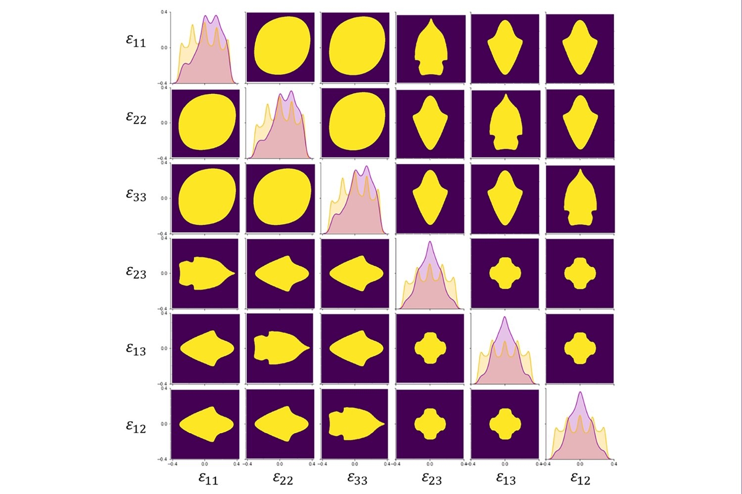
Gabrielle Wood, a junior at Howard University majoring in chemical engineering, is on a mission to improve the sustainability and life cycles of natural resources and materials. Her work in the Materials Initiative for Comprehensive Research Opportunity (MICRO) program has given her hands-on experience with many different aspects of research, including MATLAB programming, experimental design, data analysis, figure-making, and scientific writing.
Wood is also one of 10 undergraduates from 10 universities around the United States to participate in the first MICRO Summit earlier this year. The internship program, developed by the MIT Department of Materials Science and Engineering (DMSE), first launched in fall 2021. Now in its third year, the program continues to grow, providing even more opportunities for non-MIT undergraduate students — including the MICRO Summit and the program’s expansion to include Northwestern University.
“I think one of the most valuable aspects of the MICRO program is the ability to do research long term with an experienced professor in materials science and engineering,” says Wood. “My school has limited opportunities for undergraduate research in sustainable polymers, so the MICRO program allowed me to gain valuable experience in this field, which I would not otherwise have.”
Like Wood, Griheydi Garcia, a senior chemistry major at Manhattan College, values the exposure to materials science, especially since she is not able to learn as much about it at her home institution.
“I learned a lot about crystallography and defects in materials through the MICRO curriculum, especially through videos,” says Garcia. “The research itself is very valuable, as well, because we get to apply what we’ve learned through the videos in the research we do remotely.”
Expanding research opportunities
From the beginning, the MICRO program was designed as a fully remote, rigorous education and mentoring program targeted toward students from underserved backgrounds interested in pursuing graduate school in materials science or related fields. Interns are matched with faculty to work on their specific research interests.
Jessica Sandland ’99, PhD ’05, principal lecturer in DMSE and co-founder of MICRO, says that research projects for the interns are designed to be work that they can do remotely, such as developing a machine-learning algorithm or a data analysis approach.
“It’s important to note that it’s not just about what the program and faculty are bringing to the student interns,” says Sandland, a member of the MIT Digital Learning Lab, a joint program between MIT Open Learning and the Institute’s academic departments. “The students are doing real research and work, and creating things of real value. It’s very much an exchange.”
Cécile Chazot PhD ’22, now an assistant professor of materials science and engineering at Northwestern University, had helped to establish MICRO at MIT from the very beginning. Once at Northwestern, she quickly realized that expanding MICRO to Northwestern would offer even more research opportunities to interns than by relying on MIT alone — leveraging the university’s strong materials science and engineering department, as well as offering resources for biomaterials research through Northwestern’s medical school. The program received funding from 3M and officially launched at Northwestern in fall 2023. Approximately half of the MICRO interns are now in the program with MIT and half are with Northwestern. Wood and Garcia both participate in the program via Northwestern.
“By expanding to another school, we’ve been able to have interns work with a much broader range of research projects,” says Chazot. “It has become easier for us to place students with faculty and research that match their interests.”
Building community
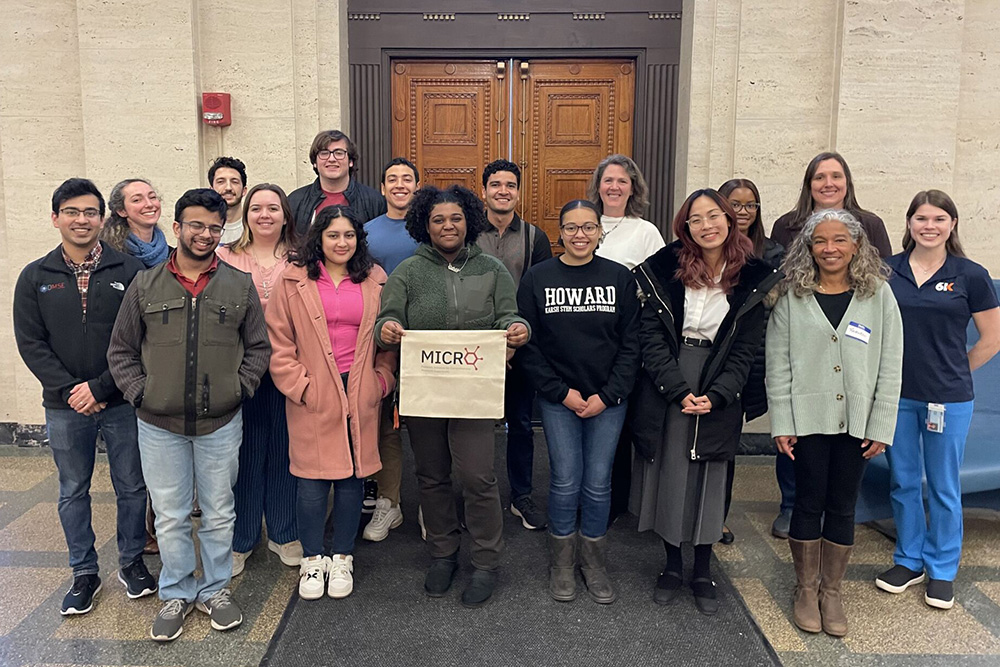
The MICRO program received a Higher Education Innovation grant from the Abdul Latif Jameel World Education Lab, part of MIT Open Learning, to develop an in-person summit. In January 2024, interns visited MIT for three days of presentations, workshops, and campus tours — including a tour of the MIT.nano building — as well as various community-building activities.
“A big part of MICRO is the community,” says Chazot. “A highlight of the summit was just seeing the students come together.”
The summit also included panel discussions that allowed interns to gain insights and advice from graduate students and professionals. The graduate panel discussion included MIT graduate students Sam Figueroa (mechanical engineering), Isabella Caruso (DMSE), and Eliana Feygin (DMSE). The career panel was led by Chazot and included Jatin Patil PhD ’23, head of product at SiTration; Maureen Reitman ’90, ScD ’93, group vice president and principal engineer at Exponent; Lucas Caretta PhD ’19, assistant professor of engineering at Brown University; Raquel D’Oyen ’90, who holds a PhD from Northwestern University and is a senior engineer at Raytheon; and Ashley Kaiser MS ’19, PhD ’21, senior process engineer at 6K.
Students also had an opportunity to share their work with each other through research presentations. Their presentations covered a wide range of topics, including: developing a computer program to calculate solubility parameters for polymers used in textile manufacturing; performing a life-cycle analysis of a photonic chip and evaluating its environmental impact in comparison to a standard silicon microchip; and applying machine learning algorithms to scanning transmission electron microscopy images of CrSBr, a two-dimensional magnetic material.
“The summit was wonderful and the best academic experience I have had as a first-year college student,” says MICRO intern Gabriella La Cour, who is pursuing a major in chemistry and dual degree biomedical engineering at Spelman College and participates in MICRO through MIT. “I got to meet so many students who were all in grades above me … and I learned a little about how to navigate college as an upperclassman.”
“I actually have an extremely close friendship with one of the students, and we keep in touch regularly,” adds La Cour. “Professor Chazot gave valuable advice about applications and recommendation letters that will be useful when I apply to REUs [Research Experiences for Undergraduates] and graduate schools.”
Looking to the future, MICRO organizers hope to continue to grow the program’s reach.
“We would love to see other schools taking on this model,” says Sandland. “There are a lot of opportunities out there. The more departments, research groups, and mentors that get involved with this program, the more impact it can have.”
![]()
© Photo courtesy of the DMSE