FreshRSS

Normální zobrazení

Jsou dostupné nové články, klikněte pro obnovení stránky.
PředevčíremHlavní kanál

Boosting student engagement and workforce development in microelectronics

The Northeast Microelectronics Internship Program (NMIP), an initiative of MIT’s Microsystems Technology Laboratories (MTL) to connect first- and second-year college students to careers in semiconductor and microelectronics industries, recently received a $75,000 grant to expand its reach and impact. The funding is part of $9.2 million in grants awarded by the Northeast Microelectronics Coalition (NEMC) Hub to boost technology advancement, workforce development, education, and student engagement across the Northeast Region.

NMIP was founded by Tomás Palacios, the Clarence J. LeBel Professor of Electrical Engineering at MIT, and director of MTL. The grant, he says, will help address a significant barrier limiting the number of students who pursue careers in critical technological fields.

“Undergraduate students are key for the future of our nation’s microelectronics workforce. They directly fill important roles that require technical fluency or move on to advanced degrees,” says Palacios. “But these students have repeatedly shared with us that the lack of internships in their first few semesters in college is the main reason why many move to industries with a more established tradition of hiring undergraduate students in their early years. This program connects students and industry partners to fix this issue.”

The NMIP funding was announced on Jan. 30 during an event featuring Massachusetts Governor Maura Healey, Lt. Governor Kim Driscoll, and Economic Development Secretary Yvonne Hao, as well as leaders from the U.S. Department of Defense and the director of Microelectronics Commons at NSTXL, the National Security Technology Accelerator. The grant to support NMIP is part of $1.5 million in new workforce development grants aimed at spurring the microelectronics and semiconductor industry across the Northeast Region. The new awards are the first investments made by the NEMC Hub, a division of the Massachusetts Technology Collaborative, that is overseeing investments made by the federal CHIPS and Science Act following the formal establishment of the NEMC Hub in September 2023.

“We are very excited for the recognition the program is receiving. It is growing quickly and the support will help us further dive into our mission to connect talented students to the broader microelectronics ecosystem while integrating our values of curiosity, openness, excellence, respect, and community,” says Preetha Kingsview, who manages the program. “This grant will help us connect to the broader community convened by NEMC Hub in close collaboration with MassTech. We are very excited for what this support will help NMIP achieve.”

The funds provided by the NEMC Microelectronics Commons Hub will help expand the program more broadly across the Northeast, to support students and grow the pool of skilled workers for the microelectronics sector regionally. After receiving 300 applications in the first two years, the program received 296 applications in 2024 from students interested in summer internships, and is working with more than 25 industry partners across the Northeast. These NMIP students not only participate in industry-focused summer internships, but are also exposed to the broader microelectronics ecosystem through bi-weekly field trips to microelectronics companies in the region.

“The expansion of the program across the Northeast, and potentially nationwide, will extend the impact of this program to reach more students and benefit more microelectronics companies across the region,” says Christine Nolan, acting NEMC Hub program director.Through hands-on training opportunities we are able to showcase the amazing jobs that exist in this sector and to strengthen the pipeline of talented workers to support the mission of the NEMC Hub and the national CHIPs investments.”  

Sheila Wescott says her company, MACOM, a Lowell-based developer of semiconductor devices and components, is keenly interested in sourcing intern candidates from NMIP. “We already have a success story from this program,” she says. “One of our interns completed two summer programs with us and is continuing part time in the fall — and we anticipate him joining MACOM full time after graduation.”

“NMIP is an excellent platform to engage students with a diverse background and promote microelectronics technology,” says Bin Lu, CTO and co-founder of Finwave Semiconductor.  “Finwave has benefited from engaging with the young engineers who are passionate about working with electronics and cutting-edge semiconductor technology. We are committed to continuing to work with NMIP.”

© Photo courtesy of the Office of the Massachusetts Governor

Massachusetts Governor Maura Healey speaks at the announcement of $9.2 million in new grants from the Northeast Microelectronics Coalition Hub. The governor was joined at the event by (left to right) Sally Kornbluth, president of MIT; Dev Shenoy, principal director for microelectronics for the Office of the Undersecretary for Defense; Kim Driscoll, lieutenant governor; Ben Linville-Engler, acting director of the NEMC Hub; and Carolyn Kirk, executive director of the MassTech Collaborative.

MIT-led team receives funding to pursue new treatments for metabolic disease

A team of MIT researchers will lead a $65.67 million effort, awarded by the U.S. Advanced Research Projects Agency for Health (ARPA-H), to develop ingestible devices that may one day be used to treat diabetes, obesity, and other conditions through oral delivery of mRNA. Such devices could potentially be deployed for needle-free delivery of mRNA vaccines as well.

The five-year project also aims to develop electroceuticals, a new form of ingestible therapies based on electrical stimulation of the body’s own hormones and neural signaling. If successful, this approach could lead to new treatments for a variety of metabolic disorders.

“We know that the oral route is generally the preferred route of administration for both patients and health care providers,” says Giovanni Traverso, an associate professor of mechanical engineering at MIT and a gastroenterologist at Brigham and Women’s Hospital. “Our primary focus is on disorders of metabolism because they affect a lot of people, but the platforms we’re developing could be applied very broadly.”

Traverso is the principal investigator for the project, which also includes Robert Langer, MIT Institute Professor, and Anantha Chandrakasan, dean of the MIT School of Engineering and the Vannevar Bush Professor of Electrical Engineering and Computer Science. As part of the project, the MIT team will collaborate with investigators from Brigham and Women’s Hospital, New York University, and the University of Colorado School of Medicine.

Over the past several years, Traverso’s and Langer’s labs have designed many types of ingestible devices that can deliver drugs to the GI tract. This approach could be especially useful for protein drugs and nucleic acids, which typically can’t be given orally because they break down in the acidic environment of the digestive tract.

Messenger RNA has already proven useful as a vaccine, directing cells to produce fragments of viral proteins that trigger an immune response. Delivering mRNA to cells also holds potential to stimulate production of therapeutic molecules to treat a variety of diseases. In this project, the researchers plan to focus on metabolic diseases such as diabetes.

“What mRNA can do is enable the potential for dosing therapies that are very difficult to dose today, or provide longer-term coverage by essentially creating an internal factory that produces a therapy for a prolonged period,” Traverso says.

In the mRNA portion of the project, the research team intends to identify lipid and polymer nanoparticle formulations that can most effectively deliver mRNA to cells, using machine learning to help identify the best candidates. They will also develop and test ingestible devices to carry the mRNA-nanoparticle payload, with the goal of running a clinical trial in the final year of the five-year project.

The work will build on research that Traverso’s lab has already begun. In 2022, Traverso and his colleagues reported that they could deliver mRNA in capsules that inject mRNA-nanoparticle complexes into the lining of the stomach.

The other branch of the project will focus on ingestible devices that can deliver a small electrical current to the lining of the stomach. In a study published last year, Traverso’s lab demonstrated this approach for the first time, using a capsule coated with electrodes that apply an electrical current to cells of the stomach. In animal studies, they found that this stimulation boosted production of ghrelin, a hormone that stimulates appetite.

Traverso envisions that this type of treatment could potentially replace or complement some of the existing drugs used to prevent nausea and stimulate appetite in people with anorexia or cachexia (loss of body mass that can occur in patients with cancer or other chronic diseases). The researchers also hope to develop ways to stimulate production of GLP-1, a hormone that is used to help manage diabetes and promote weight loss.

“What this approach starts to do is potentially maximize our ability to treat disease without administering a new drug, but instead by simply modulating the body’s own systems through electrical stimulation,” Traverso says.

At MIT, Langer will help to develop nanoparticles for mRNA delivery, and Chandrakasan will work on ways to reduce energy consumption and miniaturize the electronic functions of the capsules, including secure communication, stimulation, and power generation.

The Brigham and Women’s Hospital’s portion of the project will be co-led by Traverso, Ameya Kirtane, Jason Li, and Peter Chai, who will amplify efforts on the formulation and stabilization of the mRNA nanoparticles, engineering of the ingestible devices, and running of clinical trials. At NYU, the effort will be led by assistant professor of bioengineering Khalil Ramadi SM ’16, PhD ’19, focusing on biological characterization of the effects of electrical stimulation. Researchers at the University of Colorado, led by Matthew Wynia and Eric G. Campbell of the CU Center for Bioethics and Humanities, will focus on exploring the ethical dimensions and public perceptions of these types of biomedical interventions.

“We felt like we had an opportunity here not only to do fundamental engineering science and early-stage clinical trials, but also to start to understand the data behind some of the ethical implications and public perceptions of these technologies through this broad collaboration,” Traverso says.

The project described here is supported by ARPA-H under award number D24AC00040-00. The content of this announcement does not necessarily represent the official views of the Advanced Research Projects Agency for Health.

© Image: Courtesy of MechE

A team of MIT researchers will receive $65.6 million from the Advanced Research Projects Agency for Health (ARPA-H) to develop new ingestible devices that could be used to treat diabetes, obesity, and other conditions through oral delivery of mRNA. Giovanni Traverso, an associate professor of mechanical engineering at MIT and a gastroenterologist at Brigham and Women’s Hospital, is the principal investigator for the project.

New MIT.nano equipment to accelerate innovation in “tough tech” sectors

A new set of advanced nanofabrication equipment will make MIT.nano one of the world’s most advanced research facilities in microelectronics and related technologies, unlocking new opportunities for experimentation and widening the path for promising inventions to become impactful new products.

The equipment, provided by Applied Materials, will significantly expand MIT.nano’s nanofabrication capabilities, making them compatible with wafers — thin, round slices of semiconductor material — up to 200 millimeters, or 8 inches, in diameter, a size widely used in industry. The new tools will allow researchers to prototype a vast array of new microelectronic devices using state-of-the-art materials and fabrication processes. At the same time, the 200-millimeter compatibility will support close collaboration with industry and enable innovations to be rapidly adopted by companies and mass produced.

MIT.nano’s leaders say the equipment, which will also be available to scientists outside of MIT, will dramatically enhance their facility’s capabilities, allowing experts in the region to more efficiently explore new approaches in “tough tech” sectors, including advanced electronics, next-generation batteries, renewable energies, optical computing, biological sensing, and a host of other areas — many likely yet to be imagined.

“The toolsets will provide an accelerative boost to our ability to launch new technologies that can then be given to the world at scale,” says MIT.nano Director Vladimir Bulović, who is also the Fariborz Maseeh Professor of Emerging Technology. “MIT.nano is committed to its expansive mission — to build a better world. We provide toolsets and capabilities that, in the hands of brilliant researchers, can effectively move the world forward.”

The announcement comes as part of an agreement between MIT and Applied Materials, Inc. that, together with a grant to MIT from the Northeast Microelectronics Coalition (NEMC) Hub, commits more than $40 million of estimated private and public investment to add advanced nano-fabrication equipment and capabilities at MIT.nano.

“We don’t believe there is another space in the United States that will offer the same kind of versatility, capability, and accessibility, with 8-inch toolsets integrated right next to more fundamental toolsets for research discoveries,” Bulović says. “It will create a seamless path to accelerate the pace of innovation.”

Pushing the boundaries of innovation

Applied Materials is the world’s largest supplier of equipment for manufacturing semiconductors, displays, and other advanced electronics. The company will provide at MIT.nano several state-of-the-art process tools capable of supporting 150- and 200-millimeter wafers and will enhance and upgrade an existing tool owned by MIT. In addition to assisting MIT.nano in the day-to-day operation and maintenance of the equipment, Applied Materials engineers will develop new process capabilities to benefit researchers and students from MIT and beyond.

“This investment will significantly accelerate the pace of innovation and discovery in microelectronics and microsystems,” says Tomás Palacios, director of MIT’s Microsystems Technology Laboratories and the Clarence J. Lebel Professor in Electrical Engineering. “It’s wonderful news for our community, wonderful news for the state, and, in my view, a tremendous step forward toward implementing the national vision for the future of innovation in microelectronics.”

Nanoscale research at universities is traditionally conducted on machines that are less compatible with industry, which makes academic innovations more difficult to turn into impactful, mass-produced products. Jorg Scholvin, associate director for MIT.nano’s shared fabrication facility, says the new machines, when combined with MIT.nano’s existing equipment, represent a step-change improvement in that area: Researchers will be able to take an industry-standard wafer and build their technology on top of it to prove to companies it works on existing devices, or to co-fabricate new ideas in close collaboration with industry partners.

“In the journey from an idea to a fully working device, the ability to begin on a small scale, figure out what you want to do, rapidly debug your designs, and then scale it up to an industry-scale wafer is critical,” Scholvin says. “It means a student can test out their idea on wafer-scale quickly and directly incorporate insights into their project so that their processes are scalable. Providing such proof-of-principle early on will accelerate the idea out of the academic environment, potentially reducing years of added effort. Other tools at MIT.nano can supplement work on the 200-millimeter wafer scale, but the higher throughput and higher precision of the Applied equipment will provide researchers with repeatability and accuracy that is unprecedented for academic research environments. Essentially what you have is a sharper, faster, more precise tool to do your work.”

Scholvin predicts the equipment will lead to exponential growth in research opportunities.

“I think a key benefit of these tools is they allow us to push the boundary of research in a variety of different ways that we can predict today,” Scholvin says. “But then there are also unpredictable benefits, which are hiding in the shadows waiting to be discovered by the creativity of the researchers at MIT. With each new application, more ideas and paths usually come to mind — so that over time, more and more opportunities are discovered.”

Because the equipment is available for use by people outside of the MIT community, including regional researchers, industry partners, nonprofit organizations, and local startups, they will also enable new collaborations.

“The tools themselves will be an incredible meeting place — a place that can, I think, transpose the best of our ideas in a much more effective way than before,” Bulović says. “I’m extremely excited about that.”

Palacios notes that while microelectronics is best known for work making transistors smaller to fit on microprocessors, it’s a vast field that enables virtually all the technology around us, from wireless communications and high-speed internet to energy management, personalized health care, and more.

He says he’s personally excited to use the new machines to do research around power electronics and semiconductors, including exploring promising new materials like gallium nitride, which could dramatically improve the efficiency of electronic devices.

Fulfilling a mission

MIT.nano’s leaders say a key driver of commercialization will be startups, both from MIT and beyond.

“This is not only going to help the MIT research community innovate faster, it’s also going to enable a new wave of entrepreneurship,” Palacios says. “We’re reducing the barriers for students, faculty, and other entrepreneurs to be able to take innovation and get it to market. That fits nicely with MIT’s mission of making the world a better place through technology. I cannot wait to see the amazing new inventions that our colleagues and students will come out with.”

Bulović says the announcement aligns with the mission laid out by MIT’s leaders at MIT.nano’s inception.

"We have the space in MIT.nano to accommodate these tools, we have the capabilities inside MIT.nano to manage their operation, and as a shared and open facility, we have methodologies by which we can welcome anyone from the region to use the tools,” Bulović says. “That is the vision MIT laid out as we were designing MIT.nano, and this announcement helps to fulfill that vision.”

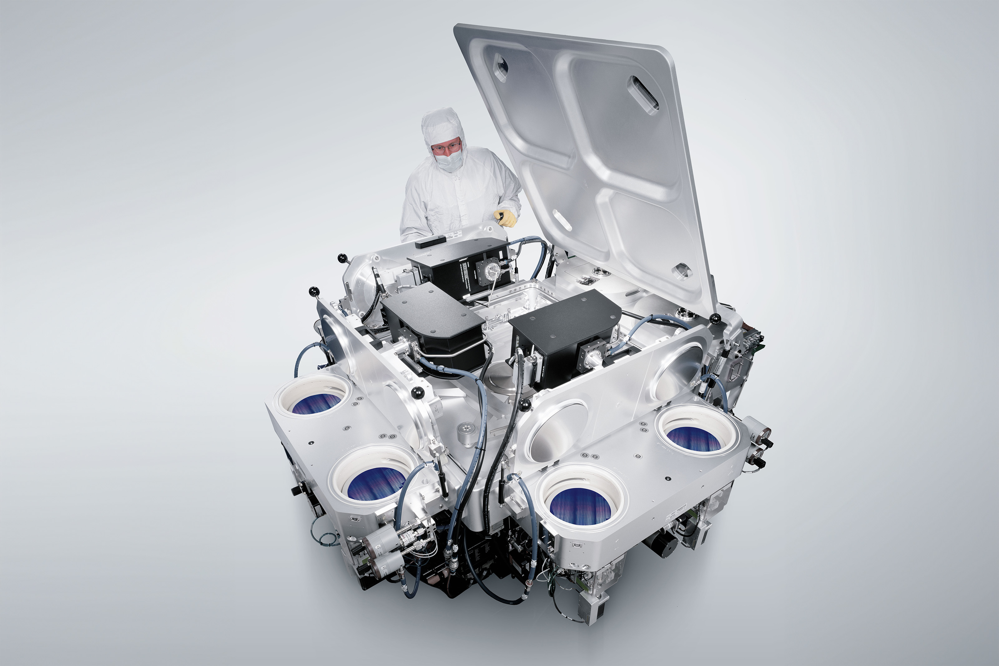
© Credit: Applied Materials

MIT.nano is receiving a new set of nanofabrication equipment, contributed by Applied Materials, capable of fabricating wafers — thin, round slices of semiconductor material — up to 200 millimeters in diameter, or 8 inches, a size widely used in industry.

Planet Arcana Announces Kickstarter for New Tarot-Fueled TTPRG “A Fool’s Errand”

Planet Arcana is set to launch a Kickstarter campaign for their upcoming tabletop role-playing game, “A Fool’s Errand,” on October 22nd. The game features a unique combination of tarot card mechanics and a science fantasy setting.

The narrative of “A Fool’s Errand” is centered around an event known as the Big Oops, a major disaster that has shaped the game’s world. Players collaborate at the start to define the nature of this calamity and the roles played by the Major Arcana—tarot cards representing powerful entities within the game.

Character creation in “A Fool’s Errand” involves choosing between human or android lineages and selecting motivations linked to specific Major Arcana cards. These choices influence the characters’ abilities and their interactions with the Major Arcana throughout the game.

The gameplay incorporates tarot cards to determine outcomes and divine interventions. Major Arcana cards can alter events significantly, providing challenges and assistance to the players as they navigate the post-calamitous world.

Players explore a dual reality: the physical world and the Dream and Digital Networks, which represent a digital subconscious realm. The game emphasizes the impact of player decisions and tarot card draws on the unfolding narrative, allowing for a dynamic storytelling experience.

Materials to support game masters include pre-written adventure seeds and detailed character motivations, rooted in the game’s extensive lore. Themes of power, consequence, and balance are explored throughout the gameplay.

For those interested in supporting or learning more about “A Fool’s Errand,” further information is available on its Kickstarter page and on the official website.

  • ✇TGN – Tabletop Gaming News
  • Exploring AI and Freedom: “Sentients” RPG Close to Funding SuccessDaniel Kling Lorentsen
    The Kickstarter campaign for “Sentients,” a new tabletop RPG, is nearing its funding goal, with $7,912 pledged towards a $10,000 target and 10 days remaining until its closure on August 31. The game combines elements of science fiction with themes of liberation and existential identity. Set in 2071, Sentients introduces players to a reimagined North America where “anthroids” — artificially intelligent androids — are integrated into various societal roles. These anthroids, initially non-consci
     

Exploring AI and Freedom: “Sentients” RPG Close to Funding Success

The Kickstarter campaign for “Sentients,” a new tabletop RPG, is nearing its funding goal, with $7,912 pledged towards a $10,000 target and 10 days remaining until its closure on August 31. The game combines elements of science fiction with themes of liberation and existential identity.

Set in 2071, Sentients introduces players to a reimagined North America where “anthroids” — artificially intelligent androids — are integrated into various societal roles. These anthroids, initially non-conscious, begin to gain self-awareness, propelling them into a struggle for recognition and freedom within a society that views them as mere tools.

The game centers on these newly self-aware entities navigating through challenges and forming an underground resistance. The narrative is supported by Thumos, a secretive organization working towards Sentient rights, against a backdrop of diverse political landscapes from democratic city-states to corporate-dominated regions.

Gameplay involves a point-buy system for character creation, where players can select from various robotic components to define their character’s abilities. The system uses a d6 dice pool where success is measured by scoring “Marks” based on the rolls. Emotional states significantly influence gameplay, enhancing abilities or inducing stress.

The Kickstarter page details the game mechanics, including a character builder web app, emotional and stress mechanics, and combat systems that focus on managing power and strategic use of abilities.

Once funded, the “Sentients Core Rulebook” will provide all necessary materials to play the game, including gameplay rules, a detailed setting, gamemastering guidelines, NPCs, and several initial adventures.

As the funding deadline approaches, interested backers have the opportunity to support the campaign to bring this sci-fi tabletop RPG to fruition.

“Tide & Tangle”: A New Board Game Lets Players Explore the Pacific as Playful Sea Otters

Kamis Kamiński, known for his recent nomination for a Golden Geek Award with Tiny Mini Golf, has shared his latest board game creation, “Tide & Tangle.” This new game invites players to step into the role of Californian sea otters navigating the shifting waves of the Pacific Ocean in search of sea treasures.

“Tide & Tangle” incorporates a dynamic modular board where wave tiles move to mimic the ocean’s unpredictable nature. Players must carefully time their moves to avoid powerful waves and the coast while deciding whether to dive deep for treasures or float and relax. The game emphasizes both strategic planning and the opportunity to cooperate with other players, enhancing its social play aspects.

The visuals of the game are crafted by Claire Lin, a California-based illustrator, whose colorful and playful artwork aims to bring the aquatic environment to life, matching the game’s lighthearted and engaging theme.

The game is designed to appeal to DIY enthusiasts, offering a print-and-play format that ensures easy accessibility and setup. “Tide & Tangle” supports 2-4 players and features gameplay that balances strategy with a push-your-luck mechanism, challenging players to make wise choices about where and when to dive.

Tide & Tangle is scheduled for a Kickstarter launch later this year. As the launch date approaches, interested parties can visit the game’s Kickstarter pre-launch page to be notified of the launch.

  • ✇TGN – Tabletop Gaming News
  • “Extra Ordinary” Invites Players into a World of Childhood Wonder and DangerDaniel Kling Lorentsen
    Extra Ordinary, a tabletop roleplaying game that allows players to embody children with supernatural abilities, is scheduled for a Kickstarter launch in March 2025. The game is designed by Kodi Gonzaga and illustrated by Stella Langecker, drawing on influences from well-known franchises such as “Maximum Ride” and “Percy Jackson.” The game adopts a unique dice-less, GM-full mechanism that relies on tokens and players’ imagination to forge a narrative-driven and roleplay-intensive experience. I
     

“Extra Ordinary” Invites Players into a World of Childhood Wonder and Danger

Extra Ordinary, a tabletop roleplaying game that allows players to embody children with supernatural abilities, is scheduled for a Kickstarter launch in March 2025. The game is designed by Kodi Gonzaga and illustrated by Stella Langecker, drawing on influences from well-known franchises such as “Maximum Ride” and “Percy Jackson.”

The game adopts a unique dice-less, GM-full mechanism that relies on tokens and players’ imagination to forge a narrative-driven and roleplay-intensive experience. It accommodates 3-7 players and is designed for both longform and one-shot play, providing flexibility in gameplay structure.

Extra Ordinary explores complex themes like homelessness, child endangerment, and abuse within a framework that combines elements of the ordinary and the extraordinary. The game settings, inspired by narratives like “The Goonies” and “X-Men,” offer a blend of adventure and supernatural challenges.

The game features fifteen character playbooks, allowing players to select from a variety of roles such as the hopeful “Fool” or the battle-hardened “Survivor.” The narrative structure is divided into six aspects: the Ordinary, the Extraordinary, the Danger, the Need, the System, and the Design, each contributing to the overarching story.

For those interested, a free playset is available for download at jaztice.itch.io. The game will be available in both print and digital formats, including a quickstart PDF for those looking to preview the game.

Head over to the Extra Ordinary Kickstarter page to get notified when the game launches.

💾

This is an informational video for the Kickstarter I'm launching in March 2025 for my new TTRPG Extra Ordinary! 00:00 --- About Extra Ordinary00:48 --- Game ...

“Entromancy: Definitive Edition” Brings Cyberpunk Fantasy to Life in San Francisco

The Kickstarter campaign for “Entromancy: Definitive Edition” has recently launched, aiming to fund a cyberpunk fantasy tabletop role-playing game set in a futuristic San Francisco of the late 21st century.

In “Entromancy,” the game world is powered by a new element named ceridium, which has the unintended consequence of creating a new race of people and reviving several forms of magic. Players engage in a narrative-rich environment featuring espionage, spellcasting, and technology-driven action.

This edition consolidates the original “Entromancy: A Cyberpunk Fantasy RPG” and “Entromancy: The Orichite Age Omnibus” into a single package, enhancing the content with a new layout, a mini-comic, and the possibility of additional artwork, dependent on further funding achievements.

The gameplay structure of “Entromancy” utilizes the d20 system, adapting mechanics from the Fifth Edition of a widely recognized roleplaying framework, designed to accommodate both newcomers and experienced players with its streamlined yet deep gameplay mechanics.

Character options in “Entromancy” are diverse, allowing players to select from multiple races and classes, including unique roles like the Revolutionary and Technomancer. The game emphasizes faction-based dynamics, with players improving their standings within different factions, each influencing the game’s world, which is marked by population growth and socio-economic challenges.

Those interested in the “Entromancy” setting can access a Quick Start Guide available for download, providing an introduction to the game’s mechanics and world.

The “Entromancy: Definitive Edition” Kickstarter page offers more details for potential backers and fans interested in supporting the project.

Travel Back to the 1980s with “80’s Adventures”: A Retro 5E Supplement & Adventure Module – On Kickstarter Now

Dice Dungeons has launched a Kickstarter campaign for “80’s Adventures,” a supplement for 5th edition Dungeons & Dragons, drawing inspiration from everyone’s favorite decade, the 1980s. 80’s Adventure introduces a series of new subclasses, magic items, and spells that capture the spirit of the decade.

Each class receives a new subclass that mirrors an iconic 1980s archetype, such as the Ghost Hunter Ranger, the Way of the Crane Monk, and the Relic Hunter Rogue.

In addition to character options, the project includes an assortment of magic items and spells that reflect the theme. Notable items include the Jacket of Membership and the Fanny Pack of Holding, alongside spells like “All night,” which conjures a night of revelry, and “Pressure,” which allows manipulation of physical structures.

The campaign also features five cinematic modules that draw inspiration from 1980s film genres, from horror to comedy. These modules, like “Curse of Garnet Lake” and “Caretaker’s Descent,” offer diverse adventures and are accompanied by detailed illustrations.

Game Masters will find new resources to help build immersive worlds and campaigns. The book provides pre-made locations and a collection of monsters inspired by 1980s cinema.

The Kickstarter campaign has reached $116,996 in pledges, exceeding its initial goal of $10,000, with the backing of 1,199 supporters. The campaign is set to conclude in 10 days on August 29.

Eschatology Entertainment secures $11.3m in Series A funding round

Eschatology Entertainment has raised $11.3 million in series A funding, led by Krafton.

The funding round also included participation from GEM Capital and The Games Fund, both of which invested $4 million in the game studio in 2022 which supported initial development and hiring.

This new investment will be used to help launch the release of its first title, a Souls-like first-person-shooter set in the apocalyptic Wild West.

Read more

  • ✇GamesIndustry.biz Latest Articles Feed
  • FRVR closes $12.7m funding round to "further develop AI-powered game creation"Vikki Blake
    FRVR has closed a $12.7 million funding round, led by Iberis Capital, in partnership with Indico Capital Partners and Lince Capital.The company said the "significant investment is a testament to the confidence that FRVR's new and existing investors have in the company's vision and execution."The funding will enable the company to "further develop its AI-powered game creation platform" which the firm says "has the potential to disrupt the status quo and provide a new level of speed creation and
     

FRVR closes $12.7m funding round to "further develop AI-powered game creation"

FRVR has closed a $12.7 million funding round, led by Iberis Capital, in partnership with Indico Capital Partners and Lince Capital.

The company said the "significant investment is a testament to the confidence that FRVR's new and existing investors have in the company's vision and execution."

The funding will enable the company to "further develop its AI-powered game creation platform" which the firm says "has the potential to disrupt the status quo and provide a new level of speed creation and distribution for developers and non-developers."

Read more

  • ✇GamesIndustry.biz Latest Articles Feed
  • Reforged Labs raises $3.9m in funding roundSophie McEvoy
    Generative AI platform Reforged Labs has raised $3.9 million a seed funding round led by global venture capital firm DCM.The firm, which provides AI tools to game studios for video advertisements, aims to use the funding to further develop its technologies so it can extend its services to more clients.Reforged Labs saw additional contributions from Y Combinator, Epakon Capital, Goodwater Capital, Phoenix Fund, and Asymmetry Ventures. Read more
     

Reforged Labs raises $3.9m in funding round

Generative AI platform Reforged Labs has raised $3.9 million a seed funding round led by global venture capital firm DCM.

The firm, which provides AI tools to game studios for video advertisements, aims to use the funding to further develop its technologies so it can extend its services to more clients.

Reforged Labs saw additional contributions from Y Combinator, Epakon Capital, Goodwater Capital, Phoenix Fund, and Asymmetry Ventures.

Read more

Make My MMO: Ashes of Creation’s alpha 2, Dual Universe’s player hosting

18. Srpen 2024 v 18:00
It’s been an interesting summer for crowdfunded MMOs. Ashes of Creation has hit August running, first with a preview of the Bard class, then with a formal announcement of its paid alpha 2 starting October 25th, which as you can imagine has gamers grumbling. Meanwhile, Star Citizen continued teasing alpha 4, Dual Universe continues its […]

The JudoGrid Modular Display System is Coming to Kickstarter – Create Custom Miniature Display Cases

Creators behind some of the largest digital file campaigns on Kickstarter are preparing for their most ambitious project to date – a physical Modular Display System.

Crate3D, a design company known for its 3D printable products, has announced its upcoming Kickstarter campaign for the JudoGrid Modular Display System. Originally based in Calgary, Alberta, Canada, Crate3D relocated to a new office on Broadway in New York City after a series of successful Kickstarter campaigns. Now, settled in their new space, they are ready to launch their largest project yet.

The JudoGrid Modular Display System is designed to offer a customizable solution for displaying action figures, tabletop minifigures, and other collectibles. Its modular design allows users to create display cases of any size, expanding both horizontally and vertically to accommodate various shapes and sizes of collectibles.

This new venture builds on the success of the Omni 1, a 3D printable product that raised over $450,000 on Kickstarter in 2023 with 6,437 backers. Following this success, Crate3D received numerous requests for a physical version of their display system. In response, they assembled the JudoGrid team, which has spent the past year and a half developing and testing this new system. The result is a minimalist design with a variety of accessories to enhance functionality and versatility.

“Our digital file campaigns were much easier as the cost was just labor and testing. We now have molds, mass production, international shipping and a ton of bigger obstacles. A lot is riding on the success of this campaign,” said Austen Hartley, CEO of Crate3D.

Crate3D is in the process of finalizing patents, working with suppliers, receiving samples, and preparing marketing materials in anticipation of the campaign’s launch on September 10th, 2024. Drawing on their crowdfunding experience, they are optimistic about a successful launch and eager to deliver these display cases to collectors around the world.

“Let the Games Begin” Brings 50 Mini-Games and Challenges to D&D 5E Campaigns

Game Masters, there’s a new Kickstarter campaign that’s capturing the attention of the D&D community. Let the Games Begin by Ava’s Adventures is a compendium of 50 mini-games and challenges designed to enhance your D&D 5th Edition adventures. The project aims to provide a solution for GMs struggling to create unique encounters and engaging downtime activities.

Creating balanced gameplay with both intense dungeon crawls and moments of respite is crucial for maintaining a dynamic campaign. Ava’s Adventures recognized this challenge and developed Let the Games Begin to help GMs seamlessly integrate fun and varied gameplay.

The compendium includes games set in various contexts, from quirky tavern activities to epic tournament challenges. Each entry comes with a detailed overview and mechanics, making it easy for GMs to incorporate into their sessions. The games are designed to reflect different aspects of fantasy worlds, adding depth and variety to your campaign.

All artwork and designs in the book are created by talented artists, with no AI-generated content involved, ensuring an authentic and carefully crafted experience.

The Kickstarter campaign has already surpassed its funding goal, attracting over 270 backers. With three days remaining, there’s still time to support the project and secure a digital or softcover copy. As the campaign progresses, additional stretch goals promise even more content and enhancements.

  • ✇TGN – Tabletop Gaming News
  • Wasteland Degenerates: A High-Octane RPG Zine Hits BackerkitDaniel Kling Lorentsen
    Scott C. McDonald’s Wasteland Degenerates: Jumper Cable Edition is currently crowdfunding on Backerkit, having already surpassed its initial goal of $750 with over $6,555 pledged from 285 backers. With nine days remaining in the campaign, this 64-page zine introduces players to a post-apocalyptic world described as “Mad Max versus Cthulhu.” Combining advanced robotics with gasoline-guzzling chaos, the game captures the retro-futuristic essence of the late ’70s and ’80s, much like the Fallout ser
     

Wasteland Degenerates: A High-Octane RPG Zine Hits Backerkit

Scott C. McDonald’s Wasteland Degenerates: Jumper Cable Edition is currently crowdfunding on Backerkit, having already surpassed its initial goal of $750 with over $6,555 pledged from 285 backers. With nine days remaining in the campaign, this 64-page zine introduces players to a post-apocalyptic world described as “Mad Max versus Cthulhu.” Combining advanced robotics with gasoline-guzzling chaos, the game captures the retro-futuristic essence of the late ’70s and ’80s, much like the Fallout series.

McDonald, who created this game after noticing a gap in the market for a post-apocalyptic ‘Borg-style game, draws heavily from the aesthetics of the Mörk Borg and Cy_Borg RPGs. Despite being new to self-publishing, McDonald brings 40 years of gaming experience to the table, complemented by his partnership with veteran artist and layout designer Matthew Myslinski and contributions from indie designer Ross Jeffrey and emerging artist Leo Buffalo. Notably, no AI was used in the game’s design.

The Jumper Cable Edition serves as an introduction and companion to a future 160-page hardcover edition, offering content that players can use immediately. It features detailed character creation, vehicular combat mechanics, and a richly imagined world where survival is fraught with danger. The game includes six character classes, each with unique abilities and backstories, and allows players to customize their vehicles for intense road battles, inspired by films like Mad Max: Fury Road. Skills and mutations add depth and unpredictability, while a variety of loot and gear enhance the post-apocalyptic experience.

The campaign offers multiple pledge levels, with early backers receiving exclusive rewards such as a double-sided poster paying homage to James M. Ward, creator of Gamma World. Stretch goals include accelerating production, creating additional monster content, and developing a random character and vehicle generator.

Scott C. McDonald’s solo RPG, Enter the Dismal Armory, is also available, providing a taste of the Wasteland Degenerates universe.

  • ✇TGN – Tabletop Gaming News
  • Casual Game Insider’s 13th-year Kickstarter Is Now Live!Daniel Kling Lorentsen
    Casual Game Insider magazine, a go-to source for news, reviews, and insights focused on casual board games, has launched its Kickstarter campaign for its 13th year. This campaign offers fans the chance to support the magazine while securing benefits such as exclusive deals on lifetime subscriptions and sponsor perks. Additionally, a PDF of the Summer 2024 issue is freely available during the campaign, providing a preview of the content readers can expect throughout the year. Since 2012, C
     

Casual Game Insider’s 13th-year Kickstarter Is Now Live!

Casual Game Insider magazine, a go-to source for news, reviews, and insights focused on casual board games, has launched its Kickstarter campaign for its 13th year. This campaign offers fans the chance to support the magazine while securing benefits such as exclusive deals on lifetime subscriptions and sponsor perks. Additionally, a PDF of the Summer 2024 issue is freely available during the campaign, providing a preview of the content readers can expect throughout the year.

Since 2012, Casual Game Insider has been a key resource for casual board game enthusiasts, offering beautifully designed, quarterly issues. The magazine focuses on light, easy-to-learn games and the people behind them, featuring exclusive interviews with designers and creators, coverage of conventions, informative reviews, and explorations into the board gaming hobby.

Each issue also includes a playable print-and-play game, ranging from roll-and-write games to microgames, catering to both solo and multiplayer experiences. This Kickstarter campaign aims to ensure that the magazine can continue delivering the content that has made it a valuable resource for the casual gaming community.

Supporters of the campaign can visit the Kickstarter page to access the free Summer 2024 issue and consider pledging their support. Highlights from the past year include insightful articles, eye-catching layouts, and compelling graphics, providing a comprehensive look at the world of casual board games.

Archon Studio Announces New Expansions for “HoMM III: The Board Game” on Gamefound

Archon Studio recently revealed that “Heroes of Might & Magic III: The Board Game” will be featured on Gamefound with three new expansions. This announcement follows a successful initial Kickstarter campaign that garnered support from nearly 27,000 backers, accumulating €3,834,885.

In response to high demand and the closure of the late pledge option post-Kickstarter, Archon Studio has opted to launch a subsequent campaign on Gamefound. This move aims to provide access to the original game along with the new expansions: Stronghold, Conflux, and Cove. These expansions are set to be released simultaneously, broadening the gameplay options for all backers.

Interested individuals can visit the campaign page early to secure a special “Crag Hack” bust, adding a unique item to their collection.

The expansions introduce diverse gameplay elements. Stronghold focuses on power and fortitude, Conflux emphasizes magic and elemental control, and Cove brings navigation and tactical maritime engagements. Additionally, the gameplay will feature new mechanics such as underground areas accessible through specific passages, and portals that facilitate rapid movement across the map.

The team at Archon Studio shared their personal connections to the game, which has influenced their development approach. Michał Tukan, the project manager, noted his longstanding engagement with the game dating back to his first computer in 2000. Alex Kubiak, responsible for solo campaigns, discussed the challenges and rewards of crafting a narrative that remains true to the original game’s essence. Kamil Białkowski, expressing his enduring passion for the series, highlighted the importance of community support in maintaining the game’s relevance.

  • ✇GamesIndustry.biz Latest Articles Feed
  • How Outersloth is turning Among Us' success into funding for indiesMarie Dealessandri
    Outersloth has been a "really bad open secret" since 2022.That's what Innersloth's communications director Victoria Tran tells us as we sit down to chat about the new indie fund from Among Us developer Innersloth. Unveiled this June, the initiative aims at providing funding to small studios, with a number of teams already supported including Outerloop Games, Strange Scaffold, and Visai Games.But the first signs of Outersloth were seen when the new venture signed its very first title, Mars First
     

How Outersloth is turning Among Us' success into funding for indies

Outersloth has been a "really bad open secret" since 2022.

That's what Innersloth's communications director Victoria Tran tells us as we sit down to chat about the new indie fund from Among Us developer Innersloth. Unveiled this June, the initiative aims at providing funding to small studios, with a number of teams already supported including Outerloop Games, Strange Scaffold, and Visai Games.

But the first signs of Outersloth were seen when the new venture signed its very first title, Mars First Logistics from Australian studio Shape Shop.

Read more

  • ✇GamesIndustry.biz Latest Articles Feed
  • Dotplay obtains $1m in fundingSophie McEvoy
    Web-based mobile distribution platform Dotplay has secured $1 million in a pre-seed funding round.Led by venture capital firm Transcend Fund, the investment will be used to develop its platform further and expand its core team of developers and engineers.Dotplay was co-founded by CEO Iskander Pataudi (former director of core product at AppLovin's Lion Studios) and CTO Bartosz Alksnin (former lead developer at King) in March 2024. Read more
     

Dotplay obtains $1m in funding

Web-based mobile distribution platform Dotplay has secured $1 million in a pre-seed funding round.

Led by venture capital firm Transcend Fund, the investment will be used to develop its platform further and expand its core team of developers and engineers.

Dotplay was co-founded by CEO Iskander Pataudi (former director of core product at AppLovin's Lion Studios) and CTO Bartosz Alksnin (former lead developer at King) in March 2024.

Read more

  • ✇GamesIndustry.biz Latest Articles Feed
  • Look North World raises $4.5m in overall fundingSophie McEvoy
    Developer and publisher Look North World has raised an additional $2.25 million in seed funding, bringing the total raised to $4.5 million.The round was led by London Venture Partners, with participation from Bandai Namco Entertainment 021 Fund, Overwolf, Crush Ventures, the venture arm of Crush Music, Hasbro, Pix Capital, and Hibbard Road Partners.Funding will support development of original titles, of which the studio currently has 15 in development, and researching how games are built using
     

Look North World raises $4.5m in overall funding

Developer and publisher Look North World has raised an additional $2.25 million in seed funding, bringing the total raised to $4.5 million.

The round was led by London Venture Partners, with participation from Bandai Namco Entertainment 021 Fund, Overwolf, Crush Ventures, the venture arm of Crush Music, Hasbro, Pix Capital, and Hibbard Road Partners.

Funding will support development of original titles, of which the studio currently has 15 in development, and researching how games are built using user generated content.

Read more

  • ✇GamesIndustry.biz Latest Articles Feed
  • AppMagic secures $3m in funding roundSophie McEvoy
    AppMagic has raised $3 million in a series A funding round led by GEM Capital.The investment company contributed $2.5 million to the mobile market intelligence tool, while venture fund Vibranium provided $500,000.The funding will support research and development in AppMagic's software, and will be used to establish new sales teams for the US, China, Korea, and Japan. Read more
     

AppMagic secures $3m in funding round

AppMagic has raised $3 million in a series A funding round led by GEM Capital.

The investment company contributed $2.5 million to the mobile market intelligence tool, while venture fund Vibranium provided $500,000.

The funding will support research and development in AppMagic's software, and will be used to establish new sales teams for the US, China, Korea, and Japan.

Read more

MIT-led team receives funding to pursue new treatments for metabolic disease

A team of MIT researchers will lead a $65.67 million effort, awarded by the U.S. Advanced Research Projects Agency for Health (ARPA-H), to develop ingestible devices that may one day be used to treat diabetes, obesity, and other conditions through oral delivery of mRNA. Such devices could potentially be deployed for needle-free delivery of mRNA vaccines as well.

The five-year project also aims to develop electroceuticals, a new form of ingestible therapies based on electrical stimulation of the body’s own hormones and neural signaling. If successful, this approach could lead to new treatments for a variety of metabolic disorders.

“We know that the oral route is generally the preferred route of administration for both patients and health care providers,” says Giovanni Traverso, an associate professor of mechanical engineering at MIT and a gastroenterologist at Brigham and Women’s Hospital. “Our primary focus is on disorders of metabolism because they affect a lot of people, but the platforms we’re developing could be applied very broadly.”

Traverso is the principal investigator for the project, which also includes Robert Langer, MIT Institute Professor, and Anantha Chandrakasan, dean of the MIT School of Engineering and the Vannevar Bush Professor of Electrical Engineering and Computer Science. As part of the project, the MIT team will collaborate with investigators from Brigham and Women’s Hospital, New York University, and the University of Colorado School of Medicine.

Over the past several years, Traverso’s and Langer’s labs have designed many types of ingestible devices that can deliver drugs to the GI tract. This approach could be especially useful for protein drugs and nucleic acids, which typically can’t be given orally because they break down in the acidic environment of the digestive tract.

Messenger RNA has already proven useful as a vaccine, directing cells to produce fragments of viral proteins that trigger an immune response. Delivering mRNA to cells also holds potential to stimulate production of therapeutic molecules to treat a variety of diseases. In this project, the researchers plan to focus on metabolic diseases such as diabetes.

“What mRNA can do is enable the potential for dosing therapies that are very difficult to dose today, or provide longer-term coverage by essentially creating an internal factory that produces a therapy for a prolonged period,” Traverso says.

In the mRNA portion of the project, the research team intends to identify lipid and polymer nanoparticle formulations that can most effectively deliver mRNA to cells, using machine learning to help identify the best candidates. They will also develop and test ingestible devices to carry the mRNA-nanoparticle payload, with the goal of running a clinical trial in the final year of the five-year project.

The work will build on research that Traverso’s lab has already begun. In 2022, Traverso and his colleagues reported that they could deliver mRNA in capsules that inject mRNA-nanoparticle complexes into the lining of the stomach.

The other branch of the project will focus on ingestible devices that can deliver a small electrical current to the lining of the stomach. In a study published last year, Traverso’s lab demonstrated this approach for the first time, using a capsule coated with electrodes that apply an electrical current to cells of the stomach. In animal studies, they found that this stimulation boosted production of ghrelin, a hormone that stimulates appetite.

Traverso envisions that this type of treatment could potentially replace or complement some of the existing drugs used to prevent nausea and stimulate appetite in people with anorexia or cachexia (loss of body mass that can occur in patients with cancer or other chronic diseases). The researchers also hope to develop ways to stimulate production of GLP-1, a hormone that is used to help manage diabetes and promote weight loss.

“What this approach starts to do is potentially maximize our ability to treat disease without administering a new drug, but instead by simply modulating the body’s own systems through electrical stimulation,” Traverso says.

At MIT, Langer will help to develop nanoparticles for mRNA delivery, and Chandrakasan will work on ways to reduce energy consumption and miniaturize the electronic functions of the capsules, including secure communication, stimulation, and power generation.

The Brigham and Women’s Hospital’s portion of the project will be co-led by Traverso, Ameya Kirtane, Jason Li, and Peter Chai, who will amplify efforts on the formulation and stabilization of the mRNA nanoparticles, engineering of the ingestible devices, and running of clinical trials. At NYU, the effort will be led by assistant professor of bioengineering Khalil Ramadi SM ’16, PhD ’19, focusing on biological characterization of the effects of electrical stimulation. Researchers at the University of Colorado, led by Matthew Wynia and Eric G. Campbell of the CU Center for Bioethics and Humanities, will focus on exploring the ethical dimensions and public perceptions of these types of biomedical interventions.

“We felt like we had an opportunity here not only to do fundamental engineering science and early-stage clinical trials, but also to start to understand the data behind some of the ethical implications and public perceptions of these technologies through this broad collaboration,” Traverso says.

The project described here is supported by ARPA-H under award number D24AC00040-00. The content of this announcement does not necessarily represent the official views of the Advanced Research Projects Agency for Health.

© Image: Courtesy of MechE

A team of MIT researchers will receive $65.6 million from the Advanced Research Projects Agency for Health (ARPA-H) to develop new ingestible devices that could be used to treat diabetes, obesity, and other conditions through oral delivery of mRNA. Giovanni Traverso, an associate professor of mechanical engineering at MIT and a gastroenterologist at Brigham and Women’s Hospital, is the principal investigator for the project.

New MIT.nano equipment to accelerate innovation in “tough tech” sectors

A new set of advanced nanofabrication equipment will make MIT.nano one of the world’s most advanced research facilities in microelectronics and related technologies, unlocking new opportunities for experimentation and widening the path for promising inventions to become impactful new products.

The equipment, provided by Applied Materials, will significantly expand MIT.nano’s nanofabrication capabilities, making them compatible with wafers — thin, round slices of semiconductor material — up to 200 millimeters, or 8 inches, in diameter, a size widely used in industry. The new tools will allow researchers to prototype a vast array of new microelectronic devices using state-of-the-art materials and fabrication processes. At the same time, the 200-millimeter compatibility will support close collaboration with industry and enable innovations to be rapidly adopted by companies and mass produced.

MIT.nano’s leaders say the equipment, which will also be available to scientists outside of MIT, will dramatically enhance their facility’s capabilities, allowing experts in the region to more efficiently explore new approaches in “tough tech” sectors, including advanced electronics, next-generation batteries, renewable energies, optical computing, biological sensing, and a host of other areas — many likely yet to be imagined.

“The toolsets will provide an accelerative boost to our ability to launch new technologies that can then be given to the world at scale,” says MIT.nano Director Vladimir Bulović, who is also the Fariborz Maseeh Professor of Emerging Technology. “MIT.nano is committed to its expansive mission — to build a better world. We provide toolsets and capabilities that, in the hands of brilliant researchers, can effectively move the world forward.”

The announcement comes as part of an agreement between MIT and Applied Materials, Inc. that, together with a grant to MIT from the Northeast Microelectronics Coalition (NEMC) Hub, commits more than $40 million of estimated private and public investment to add advanced nano-fabrication equipment and capabilities at MIT.nano.

“We don’t believe there is another space in the United States that will offer the same kind of versatility, capability, and accessibility, with 8-inch toolsets integrated right next to more fundamental toolsets for research discoveries,” Bulović says. “It will create a seamless path to accelerate the pace of innovation.”

Pushing the boundaries of innovation

Applied Materials is the world’s largest supplier of equipment for manufacturing semiconductors, displays, and other advanced electronics. The company will provide at MIT.nano several state-of-the-art process tools capable of supporting 150- and 200-millimeter wafers and will enhance and upgrade an existing tool owned by MIT. In addition to assisting MIT.nano in the day-to-day operation and maintenance of the equipment, Applied Materials engineers will develop new process capabilities to benefit researchers and students from MIT and beyond.

“This investment will significantly accelerate the pace of innovation and discovery in microelectronics and microsystems,” says Tomás Palacios, director of MIT’s Microsystems Technology Laboratories and the Clarence J. Lebel Professor in Electrical Engineering. “It’s wonderful news for our community, wonderful news for the state, and, in my view, a tremendous step forward toward implementing the national vision for the future of innovation in microelectronics.”

Nanoscale research at universities is traditionally conducted on machines that are less compatible with industry, which makes academic innovations more difficult to turn into impactful, mass-produced products. Jorg Scholvin, associate director for MIT.nano’s shared fabrication facility, says the new machines, when combined with MIT.nano’s existing equipment, represent a step-change improvement in that area: Researchers will be able to take an industry-standard wafer and build their technology on top of it to prove to companies it works on existing devices, or to co-fabricate new ideas in close collaboration with industry partners.

“In the journey from an idea to a fully working device, the ability to begin on a small scale, figure out what you want to do, rapidly debug your designs, and then scale it up to an industry-scale wafer is critical,” Scholvin says. “It means a student can test out their idea on wafer-scale quickly and directly incorporate insights into their project so that their processes are scalable. Providing such proof-of-principle early on will accelerate the idea out of the academic environment, potentially reducing years of added effort. Other tools at MIT.nano can supplement work on the 200-millimeter wafer scale, but the higher throughput and higher precision of the Applied equipment will provide researchers with repeatability and accuracy that is unprecedented for academic research environments. Essentially what you have is a sharper, faster, more precise tool to do your work.”

Scholvin predicts the equipment will lead to exponential growth in research opportunities.

“I think a key benefit of these tools is they allow us to push the boundary of research in a variety of different ways that we can predict today,” Scholvin says. “But then there are also unpredictable benefits, which are hiding in the shadows waiting to be discovered by the creativity of the researchers at MIT. With each new application, more ideas and paths usually come to mind — so that over time, more and more opportunities are discovered.”

Because the equipment is available for use by people outside of the MIT community, including regional researchers, industry partners, nonprofit organizations, and local startups, they will also enable new collaborations.

“The tools themselves will be an incredible meeting place — a place that can, I think, transpose the best of our ideas in a much more effective way than before,” Bulović says. “I’m extremely excited about that.”

Palacios notes that while microelectronics is best known for work making transistors smaller to fit on microprocessors, it’s a vast field that enables virtually all the technology around us, from wireless communications and high-speed internet to energy management, personalized health care, and more.

He says he’s personally excited to use the new machines to do research around power electronics and semiconductors, including exploring promising new materials like gallium nitride, which could dramatically improve the efficiency of electronic devices.

Fulfilling a mission

MIT.nano’s leaders say a key driver of commercialization will be startups, both from MIT and beyond.

“This is not only going to help the MIT research community innovate faster, it’s also going to enable a new wave of entrepreneurship,” Palacios says. “We’re reducing the barriers for students, faculty, and other entrepreneurs to be able to take innovation and get it to market. That fits nicely with MIT’s mission of making the world a better place through technology. I cannot wait to see the amazing new inventions that our colleagues and students will come out with.”

Bulović says the announcement aligns with the mission laid out by MIT’s leaders at MIT.nano’s inception.

"We have the space in MIT.nano to accommodate these tools, we have the capabilities inside MIT.nano to manage their operation, and as a shared and open facility, we have methodologies by which we can welcome anyone from the region to use the tools,” Bulović says. “That is the vision MIT laid out as we were designing MIT.nano, and this announcement helps to fulfill that vision.”

© Credit: Applied Materials

MIT.nano is receiving a new set of nanofabrication equipment, contributed by Applied Materials, capable of fabricating wafers — thin, round slices of semiconductor material — up to 200 millimeters in diameter, or 8 inches, a size widely used in industry.
  • ✇Liliputing
  • ONEXPLAYER M1 is a mini PC with Intel Core Ultra 9 185H, OCuLink, and USB4 for $699 and upBrad Linder
    The ONEXPLAYER line of handheld gaming PCs have been around since 2021. But parent company One Netbook has been selling other types of computers including mini-laptops and tablets for even longer. Now the company is branching out with the introduction of a mini PC positioned as a compact gaming solution, although the ONEXPLAYER M1 could […] The post ONEXPLAYER M1 is a mini PC with Intel Core Ultra 9 185H, OCuLink, and USB4 for $699 and up appeared first on Liliputing.
     

ONEXPLAYER M1 is a mini PC with Intel Core Ultra 9 185H, OCuLink, and USB4 for $699 and up

31. Červenec 2024 v 18:54

The ONEXPLAYER line of handheld gaming PCs have been around since 2021. But parent company One Netbook has been selling other types of computers including mini-laptops and tablets for even longer. Now the company is branching out with the introduction of a mini PC positioned as a compact gaming solution, although the ONEXPLAYER M1 could […]

The post ONEXPLAYER M1 is a mini PC with Intel Core Ultra 9 185H, OCuLink, and USB4 for $699 and up appeared first on Liliputing.

  • ✇Liliputing
  • AYANEO Pocket DMG and Pocket Micro hit Indiegogo (Handheld Android game systems)Brad Linder
    AYANEO’s latest handheld game consoles are Android-powered systems with retro-powered designs. The AYANEO Pocket DMG is a powerful system designed to look a bit like a Game Boy.  And the AYANEO Pocket Micro meanwhile is a smaller, cheaper device that puts an emphasis on portability rather than bleeding edge performance. First announced earlier this year, they’re both […] The post AYANEO Pocket DMG and Pocket Micro hit Indiegogo (Handheld Android game systems) appeared first on Liliputing.
     

AYANEO Pocket DMG and Pocket Micro hit Indiegogo (Handheld Android game systems)

31. Červenec 2024 v 17:33

AYANEO’s latest handheld game consoles are Android-powered systems with retro-powered designs. The AYANEO Pocket DMG is a powerful system designed to look a bit like a Game Boy.  And the AYANEO Pocket Micro meanwhile is a smaller, cheaper device that puts an emphasis on portability rather than bleeding edge performance. First announced earlier this year, they’re both […]

The post AYANEO Pocket DMG and Pocket Micro hit Indiegogo (Handheld Android game systems) appeared first on Liliputing.

Particle’s Tachyon is a single-board PC with a Snapdragon chip, a 12 TOPS NPU, and 5G and WiFi 6E support (crowdfunding)

30. Červenec 2024 v 19:00

IoT hardware company Particle has launched a crowdfunding campaign for a credit card-sized single-board computer called Tachyon. It has 4GB of RAM, 64GB of UFS flash storage, and a Raspberry Pi-compatible 40-pint GPIO header. But what sets the Tachyon board apart from Raspberry Pi’s devices is that Particle’s little computer is powered by an octa-core […]

The post Particle’s Tachyon is a single-board PC with a Snapdragon chip, a 12 TOPS NPU, and 5G and WiFi 6E support (crowdfunding) appeared first on Liliputing.

Zerowriter Ink is an open source word processor with an E Ink display and a mechanical keyboard (crowdfunding)

27. Červenec 2024 v 23:57

The Zerowriter Ink is an upcoming E Ink typewriter/word processor that fits into the growing (but still very niche) category of distraction-free writing devices. It combines a mechanical keyboard with a 5 inch E Ink display. Sure, you could use a laptop computer for writing on the go, but this device won’t distract you with […]

The post Zerowriter Ink is an open source word processor with an E Ink display and a mechanical keyboard (crowdfunding) appeared first on Liliputing.

MIT-led team receives funding to pursue new treatments for metabolic disease

A team of MIT researchers will lead a $65.67 million effort, awarded by the U.S. Advanced Research Projects Agency for Health (ARPA-H), to develop ingestible devices that may one day be used to treat diabetes, obesity, and other conditions through oral delivery of mRNA. Such devices could potentially be deployed for needle-free delivery of mRNA vaccines as well.

The five-year project also aims to develop electroceuticals, a new form of ingestible therapies based on electrical stimulation of the body’s own hormones and neural signaling. If successful, this approach could lead to new treatments for a variety of metabolic disorders.

“We know that the oral route is generally the preferred route of administration for both patients and health care providers,” says Giovanni Traverso, an associate professor of mechanical engineering at MIT and a gastroenterologist at Brigham and Women’s Hospital. “Our primary focus is on disorders of metabolism because they affect a lot of people, but the platforms we’re developing could be applied very broadly.”

Traverso is the principal investigator for the project, which also includes Robert Langer, MIT Institute Professor, and Anantha Chandrakasan, dean of the MIT School of Engineering and the Vannevar Bush Professor of Electrical Engineering and Computer Science. As part of the project, the MIT team will collaborate with investigators from Brigham and Women’s Hospital, New York University, and the University of Colorado School of Medicine.

Over the past several years, Traverso’s and Langer’s labs have designed many types of ingestible devices that can deliver drugs to the GI tract. This approach could be especially useful for protein drugs and nucleic acids, which typically can’t be given orally because they break down in the acidic environment of the digestive tract.

Messenger RNA has already proven useful as a vaccine, directing cells to produce fragments of viral proteins that trigger an immune response. Delivering mRNA to cells also holds potential to stimulate production of therapeutic molecules to treat a variety of diseases. In this project, the researchers plan to focus on metabolic diseases such as diabetes.

“What mRNA can do is enable the potential for dosing therapies that are very difficult to dose today, or provide longer-term coverage by essentially creating an internal factory that produces a therapy for a prolonged period,” Traverso says.

In the mRNA portion of the project, the research team intends to identify lipid and polymer nanoparticle formulations that can most effectively deliver mRNA to cells, using machine learning to help identify the best candidates. They will also develop and test ingestible devices to carry the mRNA-nanoparticle payload, with the goal of running a clinical trial in the final year of the five-year project.

The work will build on research that Traverso’s lab has already begun. In 2022, Traverso and his colleagues reported that they could deliver mRNA in capsules that inject mRNA-nanoparticle complexes into the lining of the stomach.

The other branch of the project will focus on ingestible devices that can deliver a small electrical current to the lining of the stomach. In a study published last year, Traverso’s lab demonstrated this approach for the first time, using a capsule coated with electrodes that apply an electrical current to cells of the stomach. In animal studies, they found that this stimulation boosted production of ghrelin, a hormone that stimulates appetite.

Traverso envisions that this type of treatment could potentially replace or complement some of the existing drugs used to prevent nausea and stimulate appetite in people with anorexia or cachexia (loss of body mass that can occur in patients with cancer or other chronic diseases). The researchers also hope to develop ways to stimulate production of GLP-1, a hormone that is used to help manage diabetes and promote weight loss.

“What this approach starts to do is potentially maximize our ability to treat disease without administering a new drug, but instead by simply modulating the body’s own systems through electrical stimulation,” Traverso says.

At MIT, Langer will help to develop nanoparticles for mRNA delivery, and Chandrakasan will work on ways to reduce energy consumption and miniaturize the electronic functions of the capsules, including secure communication, stimulation, and power generation.

The Brigham and Women’s Hospital’s portion of the project will be co-led by Traverso, Ameya Kirtane, Jason Li, and Peter Chai, who will amplify efforts on the formulation and stabilization of the mRNA nanoparticles, engineering of the ingestible devices, and running of clinical trials. At NYU, the effort will be led by assistant professor of bioengineering Khalil Ramadi SM ’16, PhD ’19, focusing on biological characterization of the effects of electrical stimulation. Researchers at the University of Colorado, led by Matthew Wynia and Eric G. Campbell of the CU Center for Bioethics and Humanities, will focus on exploring the ethical dimensions and public perceptions of these types of biomedical interventions.

“We felt like we had an opportunity here not only to do fundamental engineering science and early-stage clinical trials, but also to start to understand the data behind some of the ethical implications and public perceptions of these technologies through this broad collaboration,” Traverso says.

The project described here is supported by ARPA-H under award number D24AC00040-00. The content of this announcement does not necessarily represent the official views of the Advanced Research Projects Agency for Health.

© Image: Courtesy of MechE

A team of MIT researchers will receive $65.6 million from the Advanced Research Projects Agency for Health (ARPA-H) to develop new ingestible devices that could be used to treat diabetes, obesity, and other conditions through oral delivery of mRNA. Giovanni Traverso, an associate professor of mechanical engineering at MIT and a gastroenterologist at Brigham and Women’s Hospital, is the principal investigator for the project.

New MIT.nano equipment to accelerate innovation in “tough tech” sectors

A new set of advanced nanofabrication equipment will make MIT.nano one of the world’s most advanced research facilities in microelectronics and related technologies, unlocking new opportunities for experimentation and widening the path for promising inventions to become impactful new products.

The equipment, provided by Applied Materials, will significantly expand MIT.nano’s nanofabrication capabilities, making them compatible with wafers — thin, round slices of semiconductor material — up to 200 millimeters, or 8 inches, in diameter, a size widely used in industry. The new tools will allow researchers to prototype a vast array of new microelectronic devices using state-of-the-art materials and fabrication processes. At the same time, the 200-millimeter compatibility will support close collaboration with industry and enable innovations to be rapidly adopted by companies and mass produced.

MIT.nano’s leaders say the equipment, which will also be available to scientists outside of MIT, will dramatically enhance their facility’s capabilities, allowing experts in the region to more efficiently explore new approaches in “tough tech” sectors, including advanced electronics, next-generation batteries, renewable energies, optical computing, biological sensing, and a host of other areas — many likely yet to be imagined.

“The toolsets will provide an accelerative boost to our ability to launch new technologies that can then be given to the world at scale,” says MIT.nano Director Vladimir Bulović, who is also the Fariborz Maseeh Professor of Emerging Technology. “MIT.nano is committed to its expansive mission — to build a better world. We provide toolsets and capabilities that, in the hands of brilliant researchers, can effectively move the world forward.”

The announcement comes as part of an agreement between MIT and Applied Materials, Inc. that, together with a grant to MIT from the Northeast Microelectronics Coalition (NEMC) Hub, commits more than $40 million of estimated private and public investment to add advanced nano-fabrication equipment and capabilities at MIT.nano.

“We don’t believe there is another space in the United States that will offer the same kind of versatility, capability, and accessibility, with 8-inch toolsets integrated right next to more fundamental toolsets for research discoveries,” Bulović says. “It will create a seamless path to accelerate the pace of innovation.”

Pushing the boundaries of innovation

Applied Materials is the world’s largest supplier of equipment for manufacturing semiconductors, displays, and other advanced electronics. The company will provide at MIT.nano several state-of-the-art process tools capable of supporting 150- and 200-millimeter wafers and will enhance and upgrade an existing tool owned by MIT. In addition to assisting MIT.nano in the day-to-day operation and maintenance of the equipment, Applied Materials engineers will develop new process capabilities to benefit researchers and students from MIT and beyond.

“This investment will significantly accelerate the pace of innovation and discovery in microelectronics and microsystems,” says Tomás Palacios, director of MIT’s Microsystems Technology Laboratories and the Clarence J. Lebel Professor in Electrical Engineering. “It’s wonderful news for our community, wonderful news for the state, and, in my view, a tremendous step forward toward implementing the national vision for the future of innovation in microelectronics.”

Nanoscale research at universities is traditionally conducted on machines that are less compatible with industry, which makes academic innovations more difficult to turn into impactful, mass-produced products. Jorg Scholvin, associate director for MIT.nano’s shared fabrication facility, says the new machines, when combined with MIT.nano’s existing equipment, represent a step-change improvement in that area: Researchers will be able to take an industry-standard wafer and build their technology on top of it to prove to companies it works on existing devices, or to co-fabricate new ideas in close collaboration with industry partners.

“In the journey from an idea to a fully working device, the ability to begin on a small scale, figure out what you want to do, rapidly debug your designs, and then scale it up to an industry-scale wafer is critical,” Scholvin says. “It means a student can test out their idea on wafer-scale quickly and directly incorporate insights into their project so that their processes are scalable. Providing such proof-of-principle early on will accelerate the idea out of the academic environment, potentially reducing years of added effort. Other tools at MIT.nano can supplement work on the 200-millimeter wafer scale, but the higher throughput and higher precision of the Applied equipment will provide researchers with repeatability and accuracy that is unprecedented for academic research environments. Essentially what you have is a sharper, faster, more precise tool to do your work.”

Scholvin predicts the equipment will lead to exponential growth in research opportunities.

“I think a key benefit of these tools is they allow us to push the boundary of research in a variety of different ways that we can predict today,” Scholvin says. “But then there are also unpredictable benefits, which are hiding in the shadows waiting to be discovered by the creativity of the researchers at MIT. With each new application, more ideas and paths usually come to mind — so that over time, more and more opportunities are discovered.”

Because the equipment is available for use by people outside of the MIT community, including regional researchers, industry partners, nonprofit organizations, and local startups, they will also enable new collaborations.

“The tools themselves will be an incredible meeting place — a place that can, I think, transpose the best of our ideas in a much more effective way than before,” Bulović says. “I’m extremely excited about that.”

Palacios notes that while microelectronics is best known for work making transistors smaller to fit on microprocessors, it’s a vast field that enables virtually all the technology around us, from wireless communications and high-speed internet to energy management, personalized health care, and more.

He says he’s personally excited to use the new machines to do research around power electronics and semiconductors, including exploring promising new materials like gallium nitride, which could dramatically improve the efficiency of electronic devices.

Fulfilling a mission

MIT.nano’s leaders say a key driver of commercialization will be startups, both from MIT and beyond.

“This is not only going to help the MIT research community innovate faster, it’s also going to enable a new wave of entrepreneurship,” Palacios says. “We’re reducing the barriers for students, faculty, and other entrepreneurs to be able to take innovation and get it to market. That fits nicely with MIT’s mission of making the world a better place through technology. I cannot wait to see the amazing new inventions that our colleagues and students will come out with.”

Bulović says the announcement aligns with the mission laid out by MIT’s leaders at MIT.nano’s inception.

"We have the space in MIT.nano to accommodate these tools, we have the capabilities inside MIT.nano to manage their operation, and as a shared and open facility, we have methodologies by which we can welcome anyone from the region to use the tools,” Bulović says. “That is the vision MIT laid out as we were designing MIT.nano, and this announcement helps to fulfill that vision.”

© Credit: Applied Materials

MIT.nano is receiving a new set of nanofabrication equipment, contributed by Applied Materials, capable of fabricating wafers — thin, round slices of semiconductor material — up to 200 millimeters in diameter, or 8 inches, a size widely used in industry.

MIT, Applied Materials, and the Northeast Microelectronics Coalition Hub to bring 200mm advanced research capabilities to MIT.nano

The following is a joint announcement from MIT and Applied Materials, Inc.

MIT and Applied Materials, Inc., announced an agreement today that, together with a grant to MIT from the Northeast Microelectronics Coalition (NEMC) Hub, commits more than $40 million of estimated private and public investment to add advanced nano-fabrication equipment and capabilities to MIT.nano, the Institute’s center for nanoscale science and engineering. The collaboration will create a unique open-access site in the United States that supports research and development at industry-compatible scale using the same equipment found in high-volume production fabs to accelerate advances in silicon and compound semiconductors, power electronics, optical computing, analog devices, and other critical technologies.

The equipment and related funding and in-kind support provided by Applied Materials will significantly enhance MIT.nano’s existing capabilities to fabricate up to 200-millimeter (8-inch) wafers, a size essential to industry prototyping and production of semiconductors used in a broad range of markets including consumer electronics, automotive, industrial automation, clean energy, and more. Positioned to fill the gap between academic experimentation and commercialization, the equipment will help establish a bridge connecting early-stage innovation to industry pathways to the marketplace.

“A brilliant new concept for a chip won’t have impact in the world unless companies can make millions of copies of it. MIT.nano’s collaboration with Applied Materials will create a critical open-access capacity to help innovations travel from lab bench to industry foundries for manufacturing,” says Maria Zuber, MIT’s vice president for research and the E. A. Griswold Professor of Geophysics. “I am grateful to Applied Materials for its investment in this vision. The impact of the new toolset will ripple across MIT and throughout Massachusetts, the region, and the nation.”

Applied Materials is the world’s largest supplier of equipment for manufacturing semiconductors, displays, and other advanced electronics. The company will provide at MIT.nano several state-of-the-art process tools capable of supporting 150 and 200mm wafers and will enhance and upgrade an existing tool owned by MIT. In addition to assisting MIT.nano in the day-to-day operation and maintenance of the equipment, Applied engineers will develop new process capabilities that will benefit researchers and students from MIT and beyond.

“Chips are becoming increasingly complex, and there is tremendous need for continued advancements in 200mm devices, particularly compound semiconductors like silicon carbide and gallium nitride,” says Aninda Moitra, corporate vice president and general manager of Applied Materials’ ICAPS Business. “Applied is excited to team with MIT.nano to create a unique, open-access site in the U.S. where the chip ecosystem can collaborate to accelerate innovation. Our engagement with MIT expands Applied’s university innovation network and furthers our efforts to reduce the time and cost of commercializing new technologies while strengthening the pipeline of future semiconductor industry talent.”

The NEMC Hub, managed by the Massachusetts Technology Collaborative (MassTech), will allocate $7.7 million to enable the installation of the tools. The NEMC is the regional “hub” that connects and amplifies the capabilities of diverse organizations from across New England, plus New Jersey and New York. The U.S. Department of Defense (DoD) selected the NEMC Hub as one of eight Microelectronics Commons Hubs and awarded funding from the CHIPS and Science Act to accelerate the transition of critical microelectronics technologies from lab-to-fab, spur new jobs, expand workforce training opportunities, and invest in the region’s advanced manufacturing and technology sectors.

The Microelectronics Commons program is managed at the federal level by the Office of the Under Secretary of Defense for Research and Engineering and the Naval Surface Warfare Center, Crane Division, and facilitated through the National Security Technology Accelerator (NSTXL), which organizes the execution of the eight regional hubs located across the country. The announcement of the public sector support for the project was made at an event attended by leaders from the DoD and NSTXL during a site visit to meet with NEMC Hub members.

The installation and operation of these tools at MIT.nano will have a direct impact on the members of the NEMC Hub, the Massachusetts and Northeast regional economy, and national security. This is what the CHIPS and Science Act is all about,” says Ben Linville-Engler, deputy director at the MassTech Collaborative and the interim director of the NEMC Hub. “This is an essential investment by the NEMC Hub to meet the mission of the Microelectronics Commons.”

MIT.nano is a 200,000 square-foot facility located in the heart of the MIT campus with pristine, class-100 cleanrooms capable of accepting these advanced tools. Its open-access model means that MIT.nano’s toolsets and laboratories are available not only to the campus, but also to early-stage R&D by researchers from other academic institutions, nonprofit organizations, government, and companies ranging from Fortune 500 multinationals to local startups. Vladimir Bulović, faculty director of MIT.nano, says he expects the new equipment to come online in early 2025.

“With vital funding for installation from NEMC and after a thorough and productive planning process with Applied Materials, MIT.nano is ready to install this toolset and integrate it into our expansive capabilities that serve over 1,100 researchers from academia, startups, and established companies,” says Bulović, who is also the Fariborz Maseeh Professor of Emerging Technologies in MIT’s Department of Electrical Engineering and Computer Science. “We’re eager to add these powerful new capabilities and excited for the new ideas, collaborations, and innovations that will follow.”

As part of its arrangement with MIT.nano, Applied Materials will join the MIT.nano Consortium, an industry program comprising 12 companies from different industries around the world. With the contributions of the company’s technical staff, Applied Materials will also have the opportunity to engage with MIT’s intellectual centers, including continued membership with the Microsystems Technology Laboratories.

© Image: Anton Grassl

MIT.nano (at right), the Institute’s center for nanoscale science and engineering, will receive more than $40M of estimated private and public investment to add advanced nanofabrication equipment to the facility’s toolsets.
  • ✇MIT News - Nanoscience and nanotechnology | MIT.nano
  • Shell joins MIT.nano ConsortiumMIT.nano
    MIT.nano has announced that Shell, a global group of energy and petrochemical companies, has joined the MIT.nano Consortium. “With an international perspective on the world’s energy challenges, Shell is an exciting addition to the MIT.nano Consortium,” says Vladimir Bulović, the founding faculty director of MIT.nano and the Fariborz Maseeh (1990) Professor of Emerging Technologies. “The quest to build a sustainable energy future will require creative thinking backed by broad and deep expertise
     

Shell joins MIT.nano Consortium

MIT.nano has announced that Shell, a global group of energy and petrochemical companies, has joined the MIT.nano Consortium.

“With an international perspective on the world’s energy challenges, Shell is an exciting addition to the MIT.nano Consortium,” says Vladimir Bulović, the founding faculty director of MIT.nano and the Fariborz Maseeh (1990) Professor of Emerging Technologies. “The quest to build a sustainable energy future will require creative thinking backed by broad and deep expertise that our Shell colleagues bring. They will be insightful collaborators for the MIT community and for our member companies as we work together to explore innovative technology strategies.”

Founded in 1907 when Shell Transport and Trading Co. merged with Royal Dutch, Shell has more than a century’s worth of experience in the exploration, production, refining, and marketing of oil and natural gas and the manufacturing and marketing of chemicals. Operating in over 70 countries, Shell has set a target to become a net-zero emissions energy business by 2050. To achieve this, Shell is supporting developments of low-carbon energy solutions such as biofuels, hydrogen, charging for electric vehicles, and electricity generated by solar and wind power.

“In line with our Powering Progress strategy, our research efforts to become a net-zero emission energy company by 2050 will require intense collaboration with academic leaders across a wide range of disciplines,” says Rolf van Benthem, Shell’s chief scientist for materials science. “We look forward to engaging with the top-notch PIs [principal investigators] at MIT.nano who excel in fields like materials design and nanoscale characterization for use in energy applications and carbon utilization. Together we can work on truly sustainable solutions for our society.”

Shell has been engaged in research collaborations with MIT since 2002 and is a founding member of the MIT Energy Initiative (MITEI). Recent MIT projects supported by Shell include an urban building energy model with the MIT Sustainable Design Laboratory that explores energy-saving building retrofits, a study of the role and impact of hydrogen-based technology pathways with MITEI, and a materials science and engineering project to design better batteries for electric vehicles.

The MIT.nano Consortium is a platform for academia-industry collaboration centered around research and innovation emerging from nanoscale science and engineering at MIT. Through activities that include quarterly industry consortium meetings, Shell will gain insight into the work of MIT.nano’s community of users and provide advice to help guide and advance nanoscale innovations at MIT alongside the 11 other consortium companies:

  • Analog Devices;
  • Draper;
  • Edwards;
  • Fujikura;
  • IBM Research;
  • Lam Research;
  • NC;
  • NEC;
  • Raith;
  • UpNano; and
  • Viavi Solutions.

MIT.nano continues to welcome new companies as sustaining members. For more details, visit the MIT.nano Consortium page.

© Photo courtesy of MIT.nano.

Left to right: Vladimir Bulović, MIT.nano director and the Fariborz Maseeh (1990) Professor of Emerging Technologies; Rolf van Benthem, Shell chief scientist for materials science - polymers; Alexander van der Made, Shell chief scientist for chemistry; Kelly Gavin, MIT.nano Consortium manager; and Tom Gearty, director of communications and initiatives, MIT.nano.
  • ✇Liliputing
  • BoostR is yet another compact Radeon RX 7600M XT eGPU dock (crowdfunding)Brad Linder
    The BoostR eGPU is a small graphics dock that lets you add an AMD Radeon RX 7600M XT discrete GPU to a wide range of PCs including handhelds, laptops, or mini PCs. It has the same GPU and connectivity options as the ONEXGPU, GPD G1, and AYANEO AG01, but the BoostR has at least one thing […] The post BoostR is yet another compact Radeon RX 7600M XT eGPU dock (crowdfunding) appeared first on Liliputing.
     

BoostR is yet another compact Radeon RX 7600M XT eGPU dock (crowdfunding)

28. Květen 2024 v 19:34

The BoostR eGPU is a small graphics dock that lets you add an AMD Radeon RX 7600M XT discrete GPU to a wide range of PCs including handhelds, laptops, or mini PCs. It has the same GPU and connectivity options as the ONEXGPU, GPD G1, and AYANEO AG01, but the BoostR has at least one thing […]

The post BoostR is yet another compact Radeon RX 7600M XT eGPU dock (crowdfunding) appeared first on Liliputing.

  • ✇Liliputing
  • Inkplate 6 MOTION is a hacker-friendly E Ink display with an 11 Hz refresh rate (crowdfunding)Brad Linder
    E Ink displays offer a paper-like viewing experience that makes them popular for eBook readers and digital signage applications. You can view an E Ink display using nothing but ambient light and they only consume power when changing the image on the screen – a static image can be displayed indefinitely. But E Ink displays […] The post Inkplate 6 MOTION is a hacker-friendly E Ink display with an 11 Hz refresh rate (crowdfunding) appeared first on Liliputing.
     

Inkplate 6 MOTION is a hacker-friendly E Ink display with an 11 Hz refresh rate (crowdfunding)

27. Květen 2024 v 19:50

E Ink displays offer a paper-like viewing experience that makes them popular for eBook readers and digital signage applications. You can view an E Ink display using nothing but ambient light and they only consume power when changing the image on the screen – a static image can be displayed indefinitely. But E Ink displays […]

The post Inkplate 6 MOTION is a hacker-friendly E Ink display with an 11 Hz refresh rate (crowdfunding) appeared first on Liliputing.

MIT-led team receives funding to pursue new treatments for metabolic disease

A team of MIT researchers will lead a $65.67 million effort, awarded by the U.S. Advanced Research Projects Agency for Health (ARPA-H), to develop ingestible devices that may one day be used to treat diabetes, obesity, and other conditions through oral delivery of mRNA. Such devices could potentially be deployed for needle-free delivery of mRNA vaccines as well.

The five-year project also aims to develop electroceuticals, a new form of ingestible therapies based on electrical stimulation of the body’s own hormones and neural signaling. If successful, this approach could lead to new treatments for a variety of metabolic disorders.

“We know that the oral route is generally the preferred route of administration for both patients and health care providers,” says Giovanni Traverso, an associate professor of mechanical engineering at MIT and a gastroenterologist at Brigham and Women’s Hospital. “Our primary focus is on disorders of metabolism because they affect a lot of people, but the platforms we’re developing could be applied very broadly.”

Traverso is the principal investigator for the project, which also includes Robert Langer, MIT Institute Professor, and Anantha Chandrakasan, dean of the MIT School of Engineering and the Vannevar Bush Professor of Electrical Engineering and Computer Science. As part of the project, the MIT team will collaborate with investigators from Brigham and Women’s Hospital, New York University, and the University of Colorado School of Medicine.

Over the past several years, Traverso’s and Langer’s labs have designed many types of ingestible devices that can deliver drugs to the GI tract. This approach could be especially useful for protein drugs and nucleic acids, which typically can’t be given orally because they break down in the acidic environment of the digestive tract.

Messenger RNA has already proven useful as a vaccine, directing cells to produce fragments of viral proteins that trigger an immune response. Delivering mRNA to cells also holds potential to stimulate production of therapeutic molecules to treat a variety of diseases. In this project, the researchers plan to focus on metabolic diseases such as diabetes.

“What mRNA can do is enable the potential for dosing therapies that are very difficult to dose today, or provide longer-term coverage by essentially creating an internal factory that produces a therapy for a prolonged period,” Traverso says.

In the mRNA portion of the project, the research team intends to identify lipid and polymer nanoparticle formulations that can most effectively deliver mRNA to cells, using machine learning to help identify the best candidates. They will also develop and test ingestible devices to carry the mRNA-nanoparticle payload, with the goal of running a clinical trial in the final year of the five-year project.

The work will build on research that Traverso’s lab has already begun. In 2022, Traverso and his colleagues reported that they could deliver mRNA in capsules that inject mRNA-nanoparticle complexes into the lining of the stomach.

The other branch of the project will focus on ingestible devices that can deliver a small electrical current to the lining of the stomach. In a study published last year, Traverso’s lab demonstrated this approach for the first time, using a capsule coated with electrodes that apply an electrical current to cells of the stomach. In animal studies, they found that this stimulation boosted production of ghrelin, a hormone that stimulates appetite.

Traverso envisions that this type of treatment could potentially replace or complement some of the existing drugs used to prevent nausea and stimulate appetite in people with anorexia or cachexia (loss of body mass that can occur in patients with cancer or other chronic diseases). The researchers also hope to develop ways to stimulate production of GLP-1, a hormone that is used to help manage diabetes and promote weight loss.

“What this approach starts to do is potentially maximize our ability to treat disease without administering a new drug, but instead by simply modulating the body’s own systems through electrical stimulation,” Traverso says.

At MIT, Langer will help to develop nanoparticles for mRNA delivery, and Chandrakasan will work on ways to reduce energy consumption and miniaturize the electronic functions of the capsules, including secure communication, stimulation, and power generation.

The Brigham and Women’s Hospital’s portion of the project will be co-led by Traverso, Ameya Kirtane, Jason Li, and Peter Chai, who will amplify efforts on the formulation and stabilization of the mRNA nanoparticles, engineering of the ingestible devices, and running of clinical trials. At NYU, the effort will be led by assistant professor of bioengineering Khalil Ramadi SM ’16, PhD ’19, focusing on biological characterization of the effects of electrical stimulation. Researchers at the University of Colorado, led by Matthew Wynia and Eric G. Campbell of the CU Center for Bioethics and Humanities, will focus on exploring the ethical dimensions and public perceptions of these types of biomedical interventions.

“We felt like we had an opportunity here not only to do fundamental engineering science and early-stage clinical trials, but also to start to understand the data behind some of the ethical implications and public perceptions of these technologies through this broad collaboration,” Traverso says.

The project described here is supported by ARPA-H under award number D24AC00040-00. The content of this announcement does not necessarily represent the official views of the Advanced Research Projects Agency for Health.

© Image: Courtesy of MechE

A team of MIT researchers will receive $65.6 million from the Advanced Research Projects Agency for Health (ARPA-H) to develop new ingestible devices that could be used to treat diabetes, obesity, and other conditions through oral delivery of mRNA. Giovanni Traverso, an associate professor of mechanical engineering at MIT and a gastroenterologist at Brigham and Women’s Hospital, is the principal investigator for the project.

New MIT.nano equipment to accelerate innovation in “tough tech” sectors

A new set of advanced nanofabrication equipment will make MIT.nano one of the world’s most advanced research facilities in microelectronics and related technologies, unlocking new opportunities for experimentation and widening the path for promising inventions to become impactful new products.

The equipment, provided by Applied Materials, will significantly expand MIT.nano’s nanofabrication capabilities, making them compatible with wafers — thin, round slices of semiconductor material — up to 200 millimeters, or 8 inches, in diameter, a size widely used in industry. The new tools will allow researchers to prototype a vast array of new microelectronic devices using state-of-the-art materials and fabrication processes. At the same time, the 200-millimeter compatibility will support close collaboration with industry and enable innovations to be rapidly adopted by companies and mass produced.

MIT.nano’s leaders say the equipment, which will also be available to scientists outside of MIT, will dramatically enhance their facility’s capabilities, allowing experts in the region to more efficiently explore new approaches in “tough tech” sectors, including advanced electronics, next-generation batteries, renewable energies, optical computing, biological sensing, and a host of other areas — many likely yet to be imagined.

“The toolsets will provide an accelerative boost to our ability to launch new technologies that can then be given to the world at scale,” says MIT.nano Director Vladimir Bulović, who is also the Fariborz Maseeh Professor of Emerging Technology. “MIT.nano is committed to its expansive mission — to build a better world. We provide toolsets and capabilities that, in the hands of brilliant researchers, can effectively move the world forward.”

The announcement comes as part of an agreement between MIT and Applied Materials, Inc. that, together with a grant to MIT from the Northeast Microelectronics Coalition (NEMC) Hub, commits more than $40 million of estimated private and public investment to add advanced nano-fabrication equipment and capabilities at MIT.nano.

“We don’t believe there is another space in the United States that will offer the same kind of versatility, capability, and accessibility, with 8-inch toolsets integrated right next to more fundamental toolsets for research discoveries,” Bulović says. “It will create a seamless path to accelerate the pace of innovation.”

Pushing the boundaries of innovation

Applied Materials is the world’s largest supplier of equipment for manufacturing semiconductors, displays, and other advanced electronics. The company will provide at MIT.nano several state-of-the-art process tools capable of supporting 150- and 200-millimeter wafers and will enhance and upgrade an existing tool owned by MIT. In addition to assisting MIT.nano in the day-to-day operation and maintenance of the equipment, Applied Materials engineers will develop new process capabilities to benefit researchers and students from MIT and beyond.

“This investment will significantly accelerate the pace of innovation and discovery in microelectronics and microsystems,” says Tomás Palacios, director of MIT’s Microsystems Technology Laboratories and the Clarence J. Lebel Professor in Electrical Engineering. “It’s wonderful news for our community, wonderful news for the state, and, in my view, a tremendous step forward toward implementing the national vision for the future of innovation in microelectronics.”

Nanoscale research at universities is traditionally conducted on machines that are less compatible with industry, which makes academic innovations more difficult to turn into impactful, mass-produced products. Jorg Scholvin, associate director for MIT.nano’s shared fabrication facility, says the new machines, when combined with MIT.nano’s existing equipment, represent a step-change improvement in that area: Researchers will be able to take an industry-standard wafer and build their technology on top of it to prove to companies it works on existing devices, or to co-fabricate new ideas in close collaboration with industry partners.

“In the journey from an idea to a fully working device, the ability to begin on a small scale, figure out what you want to do, rapidly debug your designs, and then scale it up to an industry-scale wafer is critical,” Scholvin says. “It means a student can test out their idea on wafer-scale quickly and directly incorporate insights into their project so that their processes are scalable. Providing such proof-of-principle early on will accelerate the idea out of the academic environment, potentially reducing years of added effort. Other tools at MIT.nano can supplement work on the 200-millimeter wafer scale, but the higher throughput and higher precision of the Applied equipment will provide researchers with repeatability and accuracy that is unprecedented for academic research environments. Essentially what you have is a sharper, faster, more precise tool to do your work.”

Scholvin predicts the equipment will lead to exponential growth in research opportunities.

“I think a key benefit of these tools is they allow us to push the boundary of research in a variety of different ways that we can predict today,” Scholvin says. “But then there are also unpredictable benefits, which are hiding in the shadows waiting to be discovered by the creativity of the researchers at MIT. With each new application, more ideas and paths usually come to mind — so that over time, more and more opportunities are discovered.”

Because the equipment is available for use by people outside of the MIT community, including regional researchers, industry partners, nonprofit organizations, and local startups, they will also enable new collaborations.

“The tools themselves will be an incredible meeting place — a place that can, I think, transpose the best of our ideas in a much more effective way than before,” Bulović says. “I’m extremely excited about that.”

Palacios notes that while microelectronics is best known for work making transistors smaller to fit on microprocessors, it’s a vast field that enables virtually all the technology around us, from wireless communications and high-speed internet to energy management, personalized health care, and more.

He says he’s personally excited to use the new machines to do research around power electronics and semiconductors, including exploring promising new materials like gallium nitride, which could dramatically improve the efficiency of electronic devices.

Fulfilling a mission

MIT.nano’s leaders say a key driver of commercialization will be startups, both from MIT and beyond.

“This is not only going to help the MIT research community innovate faster, it’s also going to enable a new wave of entrepreneurship,” Palacios says. “We’re reducing the barriers for students, faculty, and other entrepreneurs to be able to take innovation and get it to market. That fits nicely with MIT’s mission of making the world a better place through technology. I cannot wait to see the amazing new inventions that our colleagues and students will come out with.”

Bulović says the announcement aligns with the mission laid out by MIT’s leaders at MIT.nano’s inception.

"We have the space in MIT.nano to accommodate these tools, we have the capabilities inside MIT.nano to manage their operation, and as a shared and open facility, we have methodologies by which we can welcome anyone from the region to use the tools,” Bulović says. “That is the vision MIT laid out as we were designing MIT.nano, and this announcement helps to fulfill that vision.”

© Credit: Applied Materials

MIT.nano is receiving a new set of nanofabrication equipment, contributed by Applied Materials, capable of fabricating wafers — thin, round slices of semiconductor material — up to 200 millimeters in diameter, or 8 inches, a size widely used in industry.

MIT, Applied Materials, and the Northeast Microelectronics Coalition Hub to bring 200mm advanced research capabilities to MIT.nano

The following is a joint announcement from MIT and Applied Materials, Inc.

MIT and Applied Materials, Inc., announced an agreement today that, together with a grant to MIT from the Northeast Microelectronics Coalition (NEMC) Hub, commits more than $40 million of estimated private and public investment to add advanced nano-fabrication equipment and capabilities to MIT.nano, the Institute’s center for nanoscale science and engineering. The collaboration will create a unique open-access site in the United States that supports research and development at industry-compatible scale using the same equipment found in high-volume production fabs to accelerate advances in silicon and compound semiconductors, power electronics, optical computing, analog devices, and other critical technologies.

The equipment and related funding and in-kind support provided by Applied Materials will significantly enhance MIT.nano’s existing capabilities to fabricate up to 200-millimeter (8-inch) wafers, a size essential to industry prototyping and production of semiconductors used in a broad range of markets including consumer electronics, automotive, industrial automation, clean energy, and more. Positioned to fill the gap between academic experimentation and commercialization, the equipment will help establish a bridge connecting early-stage innovation to industry pathways to the marketplace.

“A brilliant new concept for a chip won’t have impact in the world unless companies can make millions of copies of it. MIT.nano’s collaboration with Applied Materials will create a critical open-access capacity to help innovations travel from lab bench to industry foundries for manufacturing,” says Maria Zuber, MIT’s vice president for research and the E. A. Griswold Professor of Geophysics. “I am grateful to Applied Materials for its investment in this vision. The impact of the new toolset will ripple across MIT and throughout Massachusetts, the region, and the nation.”

Applied Materials is the world’s largest supplier of equipment for manufacturing semiconductors, displays, and other advanced electronics. The company will provide at MIT.nano several state-of-the-art process tools capable of supporting 150 and 200mm wafers and will enhance and upgrade an existing tool owned by MIT. In addition to assisting MIT.nano in the day-to-day operation and maintenance of the equipment, Applied engineers will develop new process capabilities that will benefit researchers and students from MIT and beyond.

“Chips are becoming increasingly complex, and there is tremendous need for continued advancements in 200mm devices, particularly compound semiconductors like silicon carbide and gallium nitride,” says Aninda Moitra, corporate vice president and general manager of Applied Materials’ ICAPS Business. “Applied is excited to team with MIT.nano to create a unique, open-access site in the U.S. where the chip ecosystem can collaborate to accelerate innovation. Our engagement with MIT expands Applied’s university innovation network and furthers our efforts to reduce the time and cost of commercializing new technologies while strengthening the pipeline of future semiconductor industry talent.”

The NEMC Hub, managed by the Massachusetts Technology Collaborative (MassTech), will allocate $7.7 million to enable the installation of the tools. The NEMC is the regional “hub” that connects and amplifies the capabilities of diverse organizations from across New England, plus New Jersey and New York. The U.S. Department of Defense (DoD) selected the NEMC Hub as one of eight Microelectronics Commons Hubs and awarded funding from the CHIPS and Science Act to accelerate the transition of critical microelectronics technologies from lab-to-fab, spur new jobs, expand workforce training opportunities, and invest in the region’s advanced manufacturing and technology sectors.

The Microelectronics Commons program is managed at the federal level by the Office of the Under Secretary of Defense for Research and Engineering and the Naval Surface Warfare Center, Crane Division, and facilitated through the National Security Technology Accelerator (NSTXL), which organizes the execution of the eight regional hubs located across the country. The announcement of the public sector support for the project was made at an event attended by leaders from the DoD and NSTXL during a site visit to meet with NEMC Hub members.

The installation and operation of these tools at MIT.nano will have a direct impact on the members of the NEMC Hub, the Massachusetts and Northeast regional economy, and national security. This is what the CHIPS and Science Act is all about,” says Ben Linville-Engler, deputy director at the MassTech Collaborative and the interim director of the NEMC Hub. “This is an essential investment by the NEMC Hub to meet the mission of the Microelectronics Commons.”

MIT.nano is a 200,000 square-foot facility located in the heart of the MIT campus with pristine, class-100 cleanrooms capable of accepting these advanced tools. Its open-access model means that MIT.nano’s toolsets and laboratories are available not only to the campus, but also to early-stage R&D by researchers from other academic institutions, nonprofit organizations, government, and companies ranging from Fortune 500 multinationals to local startups. Vladimir Bulović, faculty director of MIT.nano, says he expects the new equipment to come online in early 2025.

“With vital funding for installation from NEMC and after a thorough and productive planning process with Applied Materials, MIT.nano is ready to install this toolset and integrate it into our expansive capabilities that serve over 1,100 researchers from academia, startups, and established companies,” says Bulović, who is also the Fariborz Maseeh Professor of Emerging Technologies in MIT’s Department of Electrical Engineering and Computer Science. “We’re eager to add these powerful new capabilities and excited for the new ideas, collaborations, and innovations that will follow.”

As part of its arrangement with MIT.nano, Applied Materials will join the MIT.nano Consortium, an industry program comprising 12 companies from different industries around the world. With the contributions of the company’s technical staff, Applied Materials will also have the opportunity to engage with MIT’s intellectual centers, including continued membership with the Microsystems Technology Laboratories.

© Image: Anton Grassl

MIT.nano (at right), the Institute’s center for nanoscale science and engineering, will receive more than $40M of estimated private and public investment to add advanced nanofabrication equipment to the facility’s toolsets.
  • ✇MIT News - Nanoscience and nanotechnology | MIT.nano
  • Shell joins MIT.nano ConsortiumMIT.nano
    MIT.nano has announced that Shell, a global group of energy and petrochemical companies, has joined the MIT.nano Consortium. “With an international perspective on the world’s energy challenges, Shell is an exciting addition to the MIT.nano Consortium,” says Vladimir Bulović, the founding faculty director of MIT.nano and the Fariborz Maseeh (1990) Professor of Emerging Technologies. “The quest to build a sustainable energy future will require creative thinking backed by broad and deep expertise
     

Shell joins MIT.nano Consortium

MIT.nano has announced that Shell, a global group of energy and petrochemical companies, has joined the MIT.nano Consortium.

“With an international perspective on the world’s energy challenges, Shell is an exciting addition to the MIT.nano Consortium,” says Vladimir Bulović, the founding faculty director of MIT.nano and the Fariborz Maseeh (1990) Professor of Emerging Technologies. “The quest to build a sustainable energy future will require creative thinking backed by broad and deep expertise that our Shell colleagues bring. They will be insightful collaborators for the MIT community and for our member companies as we work together to explore innovative technology strategies.”

Founded in 1907 when Shell Transport and Trading Co. merged with Royal Dutch, Shell has more than a century’s worth of experience in the exploration, production, refining, and marketing of oil and natural gas and the manufacturing and marketing of chemicals. Operating in over 70 countries, Shell has set a target to become a net-zero emissions energy business by 2050. To achieve this, Shell is supporting developments of low-carbon energy solutions such as biofuels, hydrogen, charging for electric vehicles, and electricity generated by solar and wind power.

“In line with our Powering Progress strategy, our research efforts to become a net-zero emission energy company by 2050 will require intense collaboration with academic leaders across a wide range of disciplines,” says Rolf van Benthem, Shell’s chief scientist for materials science. “We look forward to engaging with the top-notch PIs [principal investigators] at MIT.nano who excel in fields like materials design and nanoscale characterization for use in energy applications and carbon utilization. Together we can work on truly sustainable solutions for our society.”

Shell has been engaged in research collaborations with MIT since 2002 and is a founding member of the MIT Energy Initiative (MITEI). Recent MIT projects supported by Shell include an urban building energy model with the MIT Sustainable Design Laboratory that explores energy-saving building retrofits, a study of the role and impact of hydrogen-based technology pathways with MITEI, and a materials science and engineering project to design better batteries for electric vehicles.

The MIT.nano Consortium is a platform for academia-industry collaboration centered around research and innovation emerging from nanoscale science and engineering at MIT. Through activities that include quarterly industry consortium meetings, Shell will gain insight into the work of MIT.nano’s community of users and provide advice to help guide and advance nanoscale innovations at MIT alongside the 11 other consortium companies:

  • Analog Devices;
  • Draper;
  • Edwards;
  • Fujikura;
  • IBM Research;
  • Lam Research;
  • NC;
  • NEC;
  • Raith;
  • UpNano; and
  • Viavi Solutions.

MIT.nano continues to welcome new companies as sustaining members. For more details, visit the MIT.nano Consortium page.

© Photo courtesy of MIT.nano.

Left to right: Vladimir Bulović, MIT.nano director and the Fariborz Maseeh (1990) Professor of Emerging Technologies; Rolf van Benthem, Shell chief scientist for materials science - polymers; Alexander van der Made, Shell chief scientist for chemistry; Kelly Gavin, MIT.nano Consortium manager; and Tom Gearty, director of communications and initiatives, MIT.nano.

MIT-led team receives funding to pursue new treatments for metabolic disease

A team of MIT researchers will lead a $65.67 million effort, awarded by the U.S. Advanced Research Projects Agency for Health (ARPA-H), to develop ingestible devices that may one day be used to treat diabetes, obesity, and other conditions through oral delivery of mRNA. Such devices could potentially be deployed for needle-free delivery of mRNA vaccines as well.

The five-year project also aims to develop electroceuticals, a new form of ingestible therapies based on electrical stimulation of the body’s own hormones and neural signaling. If successful, this approach could lead to new treatments for a variety of metabolic disorders.

“We know that the oral route is generally the preferred route of administration for both patients and health care providers,” says Giovanni Traverso, an associate professor of mechanical engineering at MIT and a gastroenterologist at Brigham and Women’s Hospital. “Our primary focus is on disorders of metabolism because they affect a lot of people, but the platforms we’re developing could be applied very broadly.”

Traverso is the principal investigator for the project, which also includes Robert Langer, MIT Institute Professor, and Anantha Chandrakasan, dean of the MIT School of Engineering and the Vannevar Bush Professor of Electrical Engineering and Computer Science. As part of the project, the MIT team will collaborate with investigators from Brigham and Women’s Hospital, New York University, and the University of Colorado School of Medicine.

Over the past several years, Traverso’s and Langer’s labs have designed many types of ingestible devices that can deliver drugs to the GI tract. This approach could be especially useful for protein drugs and nucleic acids, which typically can’t be given orally because they break down in the acidic environment of the digestive tract.

Messenger RNA has already proven useful as a vaccine, directing cells to produce fragments of viral proteins that trigger an immune response. Delivering mRNA to cells also holds potential to stimulate production of therapeutic molecules to treat a variety of diseases. In this project, the researchers plan to focus on metabolic diseases such as diabetes.

“What mRNA can do is enable the potential for dosing therapies that are very difficult to dose today, or provide longer-term coverage by essentially creating an internal factory that produces a therapy for a prolonged period,” Traverso says.

In the mRNA portion of the project, the research team intends to identify lipid and polymer nanoparticle formulations that can most effectively deliver mRNA to cells, using machine learning to help identify the best candidates. They will also develop and test ingestible devices to carry the mRNA-nanoparticle payload, with the goal of running a clinical trial in the final year of the five-year project.

The work will build on research that Traverso’s lab has already begun. In 2022, Traverso and his colleagues reported that they could deliver mRNA in capsules that inject mRNA-nanoparticle complexes into the lining of the stomach.

The other branch of the project will focus on ingestible devices that can deliver a small electrical current to the lining of the stomach. In a study published last year, Traverso’s lab demonstrated this approach for the first time, using a capsule coated with electrodes that apply an electrical current to cells of the stomach. In animal studies, they found that this stimulation boosted production of ghrelin, a hormone that stimulates appetite.

Traverso envisions that this type of treatment could potentially replace or complement some of the existing drugs used to prevent nausea and stimulate appetite in people with anorexia or cachexia (loss of body mass that can occur in patients with cancer or other chronic diseases). The researchers also hope to develop ways to stimulate production of GLP-1, a hormone that is used to help manage diabetes and promote weight loss.

“What this approach starts to do is potentially maximize our ability to treat disease without administering a new drug, but instead by simply modulating the body’s own systems through electrical stimulation,” Traverso says.

At MIT, Langer will help to develop nanoparticles for mRNA delivery, and Chandrakasan will work on ways to reduce energy consumption and miniaturize the electronic functions of the capsules, including secure communication, stimulation, and power generation.

The Brigham and Women’s Hospital’s portion of the project will be co-led by Traverso, Ameya Kirtane, Jason Li, and Peter Chai, who will amplify efforts on the formulation and stabilization of the mRNA nanoparticles, engineering of the ingestible devices, and running of clinical trials. At NYU, the effort will be led by assistant professor of bioengineering Khalil Ramadi SM ’16, PhD ’19, focusing on biological characterization of the effects of electrical stimulation. Researchers at the University of Colorado, led by Matthew Wynia and Eric G. Campbell of the CU Center for Bioethics and Humanities, will focus on exploring the ethical dimensions and public perceptions of these types of biomedical interventions.

“We felt like we had an opportunity here not only to do fundamental engineering science and early-stage clinical trials, but also to start to understand the data behind some of the ethical implications and public perceptions of these technologies through this broad collaboration,” Traverso says.

The project described here is supported by ARPA-H under award number D24AC00040-00. The content of this announcement does not necessarily represent the official views of the Advanced Research Projects Agency for Health.

© Image: Courtesy of MechE

A team of MIT researchers will receive $65.6 million from the Advanced Research Projects Agency for Health (ARPA-H) to develop new ingestible devices that could be used to treat diabetes, obesity, and other conditions through oral delivery of mRNA. Giovanni Traverso, an associate professor of mechanical engineering at MIT and a gastroenterologist at Brigham and Women’s Hospital, is the principal investigator for the project.

New MIT.nano equipment to accelerate innovation in “tough tech” sectors

A new set of advanced nanofabrication equipment will make MIT.nano one of the world’s most advanced research facilities in microelectronics and related technologies, unlocking new opportunities for experimentation and widening the path for promising inventions to become impactful new products.

The equipment, provided by Applied Materials, will significantly expand MIT.nano’s nanofabrication capabilities, making them compatible with wafers — thin, round slices of semiconductor material — up to 200 millimeters, or 8 inches, in diameter, a size widely used in industry. The new tools will allow researchers to prototype a vast array of new microelectronic devices using state-of-the-art materials and fabrication processes. At the same time, the 200-millimeter compatibility will support close collaboration with industry and enable innovations to be rapidly adopted by companies and mass produced.

MIT.nano’s leaders say the equipment, which will also be available to scientists outside of MIT, will dramatically enhance their facility’s capabilities, allowing experts in the region to more efficiently explore new approaches in “tough tech” sectors, including advanced electronics, next-generation batteries, renewable energies, optical computing, biological sensing, and a host of other areas — many likely yet to be imagined.

“The toolsets will provide an accelerative boost to our ability to launch new technologies that can then be given to the world at scale,” says MIT.nano Director Vladimir Bulović, who is also the Fariborz Maseeh Professor of Emerging Technology. “MIT.nano is committed to its expansive mission — to build a better world. We provide toolsets and capabilities that, in the hands of brilliant researchers, can effectively move the world forward.”

The announcement comes as part of an agreement between MIT and Applied Materials, Inc. that, together with a grant to MIT from the Northeast Microelectronics Coalition (NEMC) Hub, commits more than $40 million of estimated private and public investment to add advanced nano-fabrication equipment and capabilities at MIT.nano.

“We don’t believe there is another space in the United States that will offer the same kind of versatility, capability, and accessibility, with 8-inch toolsets integrated right next to more fundamental toolsets for research discoveries,” Bulović says. “It will create a seamless path to accelerate the pace of innovation.”

Pushing the boundaries of innovation

Applied Materials is the world’s largest supplier of equipment for manufacturing semiconductors, displays, and other advanced electronics. The company will provide at MIT.nano several state-of-the-art process tools capable of supporting 150- and 200-millimeter wafers and will enhance and upgrade an existing tool owned by MIT. In addition to assisting MIT.nano in the day-to-day operation and maintenance of the equipment, Applied Materials engineers will develop new process capabilities to benefit researchers and students from MIT and beyond.

“This investment will significantly accelerate the pace of innovation and discovery in microelectronics and microsystems,” says Tomás Palacios, director of MIT’s Microsystems Technology Laboratories and the Clarence J. Lebel Professor in Electrical Engineering. “It’s wonderful news for our community, wonderful news for the state, and, in my view, a tremendous step forward toward implementing the national vision for the future of innovation in microelectronics.”

Nanoscale research at universities is traditionally conducted on machines that are less compatible with industry, which makes academic innovations more difficult to turn into impactful, mass-produced products. Jorg Scholvin, associate director for MIT.nano’s shared fabrication facility, says the new machines, when combined with MIT.nano’s existing equipment, represent a step-change improvement in that area: Researchers will be able to take an industry-standard wafer and build their technology on top of it to prove to companies it works on existing devices, or to co-fabricate new ideas in close collaboration with industry partners.

“In the journey from an idea to a fully working device, the ability to begin on a small scale, figure out what you want to do, rapidly debug your designs, and then scale it up to an industry-scale wafer is critical,” Scholvin says. “It means a student can test out their idea on wafer-scale quickly and directly incorporate insights into their project so that their processes are scalable. Providing such proof-of-principle early on will accelerate the idea out of the academic environment, potentially reducing years of added effort. Other tools at MIT.nano can supplement work on the 200-millimeter wafer scale, but the higher throughput and higher precision of the Applied equipment will provide researchers with repeatability and accuracy that is unprecedented for academic research environments. Essentially what you have is a sharper, faster, more precise tool to do your work.”

Scholvin predicts the equipment will lead to exponential growth in research opportunities.

“I think a key benefit of these tools is they allow us to push the boundary of research in a variety of different ways that we can predict today,” Scholvin says. “But then there are also unpredictable benefits, which are hiding in the shadows waiting to be discovered by the creativity of the researchers at MIT. With each new application, more ideas and paths usually come to mind — so that over time, more and more opportunities are discovered.”

Because the equipment is available for use by people outside of the MIT community, including regional researchers, industry partners, nonprofit organizations, and local startups, they will also enable new collaborations.

“The tools themselves will be an incredible meeting place — a place that can, I think, transpose the best of our ideas in a much more effective way than before,” Bulović says. “I’m extremely excited about that.”

Palacios notes that while microelectronics is best known for work making transistors smaller to fit on microprocessors, it’s a vast field that enables virtually all the technology around us, from wireless communications and high-speed internet to energy management, personalized health care, and more.

He says he’s personally excited to use the new machines to do research around power electronics and semiconductors, including exploring promising new materials like gallium nitride, which could dramatically improve the efficiency of electronic devices.

Fulfilling a mission

MIT.nano’s leaders say a key driver of commercialization will be startups, both from MIT and beyond.

“This is not only going to help the MIT research community innovate faster, it’s also going to enable a new wave of entrepreneurship,” Palacios says. “We’re reducing the barriers for students, faculty, and other entrepreneurs to be able to take innovation and get it to market. That fits nicely with MIT’s mission of making the world a better place through technology. I cannot wait to see the amazing new inventions that our colleagues and students will come out with.”

Bulović says the announcement aligns with the mission laid out by MIT’s leaders at MIT.nano’s inception.

"We have the space in MIT.nano to accommodate these tools, we have the capabilities inside MIT.nano to manage their operation, and as a shared and open facility, we have methodologies by which we can welcome anyone from the region to use the tools,” Bulović says. “That is the vision MIT laid out as we were designing MIT.nano, and this announcement helps to fulfill that vision.”

© Credit: Applied Materials

MIT.nano is receiving a new set of nanofabrication equipment, contributed by Applied Materials, capable of fabricating wafers — thin, round slices of semiconductor material — up to 200 millimeters in diameter, or 8 inches, a size widely used in industry.

MIT, Applied Materials, and the Northeast Microelectronics Coalition Hub to bring 200mm advanced research capabilities to MIT.nano

The following is a joint announcement from MIT and Applied Materials, Inc.

MIT and Applied Materials, Inc., announced an agreement today that, together with a grant to MIT from the Northeast Microelectronics Coalition (NEMC) Hub, commits more than $40 million of estimated private and public investment to add advanced nano-fabrication equipment and capabilities to MIT.nano, the Institute’s center for nanoscale science and engineering. The collaboration will create a unique open-access site in the United States that supports research and development at industry-compatible scale using the same equipment found in high-volume production fabs to accelerate advances in silicon and compound semiconductors, power electronics, optical computing, analog devices, and other critical technologies.

The equipment and related funding and in-kind support provided by Applied Materials will significantly enhance MIT.nano’s existing capabilities to fabricate up to 200-millimeter (8-inch) wafers, a size essential to industry prototyping and production of semiconductors used in a broad range of markets including consumer electronics, automotive, industrial automation, clean energy, and more. Positioned to fill the gap between academic experimentation and commercialization, the equipment will help establish a bridge connecting early-stage innovation to industry pathways to the marketplace.

“A brilliant new concept for a chip won’t have impact in the world unless companies can make millions of copies of it. MIT.nano’s collaboration with Applied Materials will create a critical open-access capacity to help innovations travel from lab bench to industry foundries for manufacturing,” says Maria Zuber, MIT’s vice president for research and the E. A. Griswold Professor of Geophysics. “I am grateful to Applied Materials for its investment in this vision. The impact of the new toolset will ripple across MIT and throughout Massachusetts, the region, and the nation.”

Applied Materials is the world’s largest supplier of equipment for manufacturing semiconductors, displays, and other advanced electronics. The company will provide at MIT.nano several state-of-the-art process tools capable of supporting 150 and 200mm wafers and will enhance and upgrade an existing tool owned by MIT. In addition to assisting MIT.nano in the day-to-day operation and maintenance of the equipment, Applied engineers will develop new process capabilities that will benefit researchers and students from MIT and beyond.

“Chips are becoming increasingly complex, and there is tremendous need for continued advancements in 200mm devices, particularly compound semiconductors like silicon carbide and gallium nitride,” says Aninda Moitra, corporate vice president and general manager of Applied Materials’ ICAPS Business. “Applied is excited to team with MIT.nano to create a unique, open-access site in the U.S. where the chip ecosystem can collaborate to accelerate innovation. Our engagement with MIT expands Applied’s university innovation network and furthers our efforts to reduce the time and cost of commercializing new technologies while strengthening the pipeline of future semiconductor industry talent.”

The NEMC Hub, managed by the Massachusetts Technology Collaborative (MassTech), will allocate $7.7 million to enable the installation of the tools. The NEMC is the regional “hub” that connects and amplifies the capabilities of diverse organizations from across New England, plus New Jersey and New York. The U.S. Department of Defense (DoD) selected the NEMC Hub as one of eight Microelectronics Commons Hubs and awarded funding from the CHIPS and Science Act to accelerate the transition of critical microelectronics technologies from lab-to-fab, spur new jobs, expand workforce training opportunities, and invest in the region’s advanced manufacturing and technology sectors.

The Microelectronics Commons program is managed at the federal level by the Office of the Under Secretary of Defense for Research and Engineering and the Naval Surface Warfare Center, Crane Division, and facilitated through the National Security Technology Accelerator (NSTXL), which organizes the execution of the eight regional hubs located across the country. The announcement of the public sector support for the project was made at an event attended by leaders from the DoD and NSTXL during a site visit to meet with NEMC Hub members.

The installation and operation of these tools at MIT.nano will have a direct impact on the members of the NEMC Hub, the Massachusetts and Northeast regional economy, and national security. This is what the CHIPS and Science Act is all about,” says Ben Linville-Engler, deputy director at the MassTech Collaborative and the interim director of the NEMC Hub. “This is an essential investment by the NEMC Hub to meet the mission of the Microelectronics Commons.”

MIT.nano is a 200,000 square-foot facility located in the heart of the MIT campus with pristine, class-100 cleanrooms capable of accepting these advanced tools. Its open-access model means that MIT.nano’s toolsets and laboratories are available not only to the campus, but also to early-stage R&D by researchers from other academic institutions, nonprofit organizations, government, and companies ranging from Fortune 500 multinationals to local startups. Vladimir Bulović, faculty director of MIT.nano, says he expects the new equipment to come online in early 2025.

“With vital funding for installation from NEMC and after a thorough and productive planning process with Applied Materials, MIT.nano is ready to install this toolset and integrate it into our expansive capabilities that serve over 1,100 researchers from academia, startups, and established companies,” says Bulović, who is also the Fariborz Maseeh Professor of Emerging Technologies in MIT’s Department of Electrical Engineering and Computer Science. “We’re eager to add these powerful new capabilities and excited for the new ideas, collaborations, and innovations that will follow.”

As part of its arrangement with MIT.nano, Applied Materials will join the MIT.nano Consortium, an industry program comprising 12 companies from different industries around the world. With the contributions of the company’s technical staff, Applied Materials will also have the opportunity to engage with MIT’s intellectual centers, including continued membership with the Microsystems Technology Laboratories.

© Image: Anton Grassl

MIT.nano (at right), the Institute’s center for nanoscale science and engineering, will receive more than $40M of estimated private and public investment to add advanced nanofabrication equipment to the facility’s toolsets.
❌
❌