FreshRSS

Normální zobrazení

Jsou dostupné nové články, klikněte pro obnovení stránky.
PředevčíremHlavní kanál
  • ✇MIT News - Nanoscience and nanotechnology | MIT.nano
  • Propelling atomically layered magnets toward green computersMedia Lab
    Globally, computation is booming at an unprecedented rate, fueled by the boons of artificial intelligence. With this, the staggering energy demand of the world’s computing infrastructure has become a major concern, and the development of computing devices that are far more energy-efficient is a leading challenge for the scientific community.  Use of magnetic materials to build computing devices like memories and processors has emerged as a promising avenue for creating “beyond-CMOS” computers,
     

Propelling atomically layered magnets toward green computers

Globally, computation is booming at an unprecedented rate, fueled by the boons of artificial intelligence. With this, the staggering energy demand of the world’s computing infrastructure has become a major concern, and the development of computing devices that are far more energy-efficient is a leading challenge for the scientific community. 

Use of magnetic materials to build computing devices like memories and processors has emerged as a promising avenue for creating “beyond-CMOS” computers, which would use far less energy compared to traditional computers. Magnetization switching in magnets can be used in computation the same way that a transistor switches from open or closed to represent the 0s and 1s of binary code. 

While much of the research along this direction has focused on using bulk magnetic materials, a new class of magnetic materials — called two-dimensional van der Waals magnets — provides superior properties that can improve the scalability and energy efficiency of magnetic devices to make them commercially viable. 

Although the benefits of shifting to 2D magnetic materials are evident, their practical induction into computers has been hindered by some fundamental challenges. Until recently, 2D magnetic materials could operate only at very low temperatures, much like superconductors. So bringing their operating temperatures above room temperature has remained a primary goal. Additionally, for use in computers, it is important that they can be controlled electrically, without the need for magnetic fields. Bridging this fundamental gap, where 2D magnetic materials can be electrically switched above room temperature without any magnetic fields, could potentially catapult the translation of 2D magnets into the next generation of “green” computers.

A team of MIT researchers has now achieved this critical milestone by designing a “van der Waals atomically layered heterostructure” device where a 2D van der Waals magnet, iron gallium telluride, is interfaced with another 2D material, tungsten ditelluride. In an open-access paper published March 15 in Science Advances, the team shows that the magnet can be toggled between the 0 and 1 states simply by applying pulses of electrical current across their two-layer device. 

“Our device enables robust magnetization switching without the need for an external magnetic field, opening up unprecedented opportunities for ultra-low power and environmentally sustainable computing technology for big data and AI,” says lead author Deblina Sarkar, the AT&T Career Development Assistant Professor at the MIT Media Lab and Center for Neurobiological Engineering, and head of the Nano-Cybernetic Biotrek research group. “Moreover, the atomically layered structure of our device provides unique capabilities including improved interface and possibilities of gate voltage tunability, as well as flexible and transparent spintronic technologies.”

Sarkar is joined on the paper by first author Shivam Kajale, a graduate student in Sarkar’s research group at the Media Lab; Thanh Nguyen, a graduate student in the Department of Nuclear Science and Engineering (NSE); Nguyen Tuan Hung, an MIT visiting scholar in NSE and an assistant professor at Tohoku University in Japan; and Mingda Li, associate professor of NSE.

Breaking the mirror symmetries 

When electric current flows through heavy metals like platinum or tantalum, the electrons get segregated in the materials based on their spin component, a phenomenon called the spin Hall effect, says Kajale. The way this segregation happens depends on the material, and particularly its symmetries.

“The conversion of electric current to spin currents in heavy metals lies at the heart of controlling magnets electrically,” Kajale notes. “The microscopic structure of conventionally used materials, like platinum, have a kind of mirror symmetry, which restricts the spin currents only to in-plane spin polarization.”

Kajale explains that two mirror symmetries must be broken to produce an “out-of-plane” spin component that can be transferred to a magnetic layer to induce field-free switching. “Electrical current can 'break' the mirror symmetry along one plane in platinum, but its crystal structure prevents the mirror symmetry from being broken in a second plane.”

In their earlier experiments, the researchers used a small magnetic field to break the second mirror plane. To get rid of the need for a magnetic nudge, Kajale and Sarkar and colleagues looked instead for a material with a structure that could break the second mirror plane without outside help. This led them to another 2D material, tungsten ditelluride. The tungsten ditelluride that the researchers used has an orthorhombic crystal structure. The material itself has one broken mirror plane. Thus, by applying current along its low-symmetry axis (parallel to the broken mirror plane), the resulting spin current has an out-of-plane spin component that can directly induce switching in the ultra-thin magnet interfaced with the tungsten ditelluride. 

“Because it's also a 2D van der Waals material, it can also ensure that when we stack the two materials together, we get pristine interfaces and a good flow of electron spins between the materials,” says Kajale. 

Becoming more energy-efficient 

Computer memory and processors built from magnetic materials use less energy than traditional silicon-based devices. And the van der Waals magnets can offer higher energy efficiency and better scalability compared to bulk magnetic material, the researchers note. 

The electrical current density used for switching the magnet translates to how much energy is dissipated during switching. A lower density means a much more energy-efficient material. “The new design has one of the lowest current densities in van der Waals magnetic materials,” Kajale says. “This new design has an order of magnitude lower in terms of the switching current required in bulk materials. This translates to something like two orders of magnitude improvement in energy efficiency.”

The research team is now looking at similar low-symmetry van der Waals materials to see if they can reduce current density even further. They are also hoping to collaborate with other researchers to find ways to manufacture the 2D magnetic switch devices at commercial scale. 

This work was carried out, in part, using the facilities at MIT.nano. It was funded by the Media Lab, the U.S. National Science Foundation, and the U.S. Department of Energy.

© Image courtesy of the researchers.

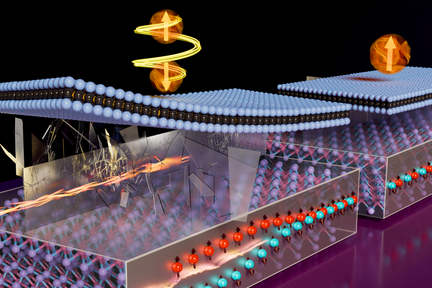
The flow of electrical current in the bottom crystalline slab (representing WTe2) breaks a mirror symmetry (shattered glass), while the material itself breaks the other mirror symmetry (cracked glass). The resulting spin current has vertical polarization that switches the magnetic state of the top 2D ferromagnet.

Creative collisions: Crossing the art-science divide

MIT has a rich history of productive collaboration between the arts and the sciences, anchored by the conviction that these two conventionally opposed ways of thinking can form a deeply generative symbiosis that serves to advance and humanize new technologies. 

This ethos was made tangible when the Bauhaus artist and educator György Kepes established the MIT Center for Advanced Visual Studies (CAVS) within the Department of Architecture in 1967. CAVS has since evolved into the Art, Culture, and Technology (ACT) program, which fosters close links to multiple other programs, centers, and labs at MIT. Class 4.373/4.374 (Creating Art, Thinking Science), open to undergraduates and master’s students of all disciplines as well as certain students from the Harvard Graduate School of Design (GSD), is one of the program’s most innovative offerings, proposing a model for how the relationship between art and science might play out at a time of exponential technological growth. 

Now in its third year, the class is supported by an Interdisciplinary Class Development Grant from the MIT Center for Art, Science and Technology (CAST) and draws upon the unparalleled resources of MIT.nano; an artist’s high-tech toolbox for investigating the hidden structures and beauty of our material universe.

High ambitions and critical thinking

The class was initiated by Tobias Putrih, lecturer in ACT, and is taught with the assistance of Ardalan SadeghiKivi MArch ’23, and Aubrie James SM ’24. Central to the success of the class has been the collaboration with co-instructor Vladimir Bulović, the founding director of MIT.nano and Fariborz Maseeh Chair in Emerging Technology, who has positioned the facility as an open-access resource for the campus at large — including MIT’s community of artists. “Creating Art, Thinking Science” unfolds the 100,000 square feet of cleanroom and lab space within the Lisa T. Su Building, inviting participating students to take advantage of cutting-edge equipment for nanoscale visualization and fabrication; in the hands of artists, devices for discovering nanostructures and manipulating atoms become tools for rendering the invisible visible and deconstructing the dynamics of perception itself. 

The expansive goals of the class are tempered by an in-built criticality. “ACT has a unique position as an art program nested within a huge scientific institute — and the challenges of that partnership should not be underestimated,” reflects Putrih. “Science and art are wholly different knowledge systems with distinct historical perspectives. So, how do we communicate? How do we locate that middle ground, that third space?”

An evolving answer, tested and developed throughout the partnership between ACT and MIT.nano, involves a combination of attentive mentorship and sharing of artistic ideas, combined with access to advanced technological resources and hands-on practical training. 

“MIT.nano currently accommodates more than 1,200 individuals to do their work, across 250 different research groups,” says Bulović. “The fact that we count artists among those is a matter of pride for us. We’ve found that the work of our scientists and technologists is enhanced by having access to the language of art as a form of expression — equally, the way that artists express themselves can be stretched beyond what could previously be imagined, simply by having access to the tools and instruments at MIT.nano.”

A playground for experimentation

True to the spirit of the scientific method and artistic iteration, the class is envisioned as a work in progress — a series of propositions and prototypes for how dialogue between scientists and artists might work in practice. The outcomes of those experiments can now be seen installed in the first and second floor galleries at MIT.nano. As part of the facility’s five-year anniversary celebration, the class premiered an exhibition showcasing works created during previous years of “Creating Art, Thinking Science.” 

Visitors to the exhibition, “zero.zerozerozerozerozerozerozerozeroone” (named for the numerical notation for one nanometer), will encounter artworks ranging from a minimalist silicon wafer produced with two-photon polymerization (2PP) technology (“Obscured Invisibility,” 2021, Hyun Woo Park), to traces of an attempt to make vegetable soup in the cleanroom using equipment such as a cryostat, a fluorescing microscope, and a Micro-CT scanner (“May I Please Make You Some Soup?,” 2022, Simone Lasser). 

These works set a precedent for the artworks produced during the fall 2023 iteration of the class. For Ryan Yang, in his senior year studying electrical engineering and computer science at MIT, the chance to engage in open discussion and experimental making has been a rare opportunity to “try something that might not work.” His project explores the possibilities of translating traditional block printing techniques to micron-scale 3D-printing in the MIT.nano labs.

Yang has taken advantage of the arts curriculum at MIT at an early stage in his academic career as an engineer; meanwhile, Ameen Kaleem started out as a filmmaker in New Delhi and is now pursuing a master’s degree in design engineering at Harvard GSD, cross-registered at MIT. 

Kaleem’s project models the process of abiogenesis (the evolution of living organisms from inorganic or inanimate substances) by bringing living moss into the MIT.nano cleanroom facilities to be examined at an atomic scale. “I was interested in the idea that, as a human being in the cleanroom, you are both the most sanitized version of yourself and the dirtiest thing in that space,” she reflects. “Drawing attention to the presence of organic life in the cleanroom is comparable to bringing art into spaces where it might not otherwise exist — a way of humanizing scientific and technological endeavors.”

Consciousness, immersion, and innovation

The students draw upon the legacies of landmark art-science initiatives — including international exhibitions such as “Cybernetic Serendipity” (London ICA, 1968), the “New Tendencies” series (Zagreb, 1961-73), and “Laboratorium” (Antwerp, 1999) — and take inspiration from the instructors’ own creative investigations of the inner workings of different knowledge systems. “In contemporary life, and at MIT in particular, we’re immersed in technology,” says Putrih. “It’s the nature of art to reveal that to us, so that we might see the implications of what we are producing and its potential impact.”

By fostering a mindset of imagination and criticality, combined with building the technical skills to address practical problems, “Creating Art, Thinking Science” seeks to create the conditions for a more expansive version of technological optimism; a culture of innovation in which social and environmental responsibility are seen as productive parameters for enriched creativity. The ripple effects of the class might be years in the making, but as Bulović observes while navigating the exhibition at MIT.nano, “The joy of the collaboration can be felt in the artworks.”

© Photo courtesy of MIT CAST.

Two students engage with an artwork created in 4.373/4.374 (Creating Art, Thinking Science).

Researchers harness 2D magnetic materials for energy-efficient computing

Experimental computer memories and processors built from magnetic materials use far less energy than traditional silicon-based devices. Two-dimensional magnetic materials, composed of layers that are only a few atoms thick, have incredible properties that could allow magnetic-based devices to achieve unprecedented speed, efficiency, and scalability.

While many hurdles must be overcome until these so-called van der Waals magnetic materials can be integrated into functioning computers, MIT researchers took an important step in this direction by demonstrating precise control of a van der Waals magnet at room temperature.

This is key, since magnets composed of atomically thin van der Waals materials can typically only be controlled at extremely cold temperatures, making them difficult to deploy outside a laboratory.

The researchers used pulses of electrical current to switch the direction of the device’s magnetization at room temperature. Magnetic switching can be used in computation, the same way a transistor switches between open and closed to represent 0s and 1s in binary code, or in computer memory, where switching enables data storage.

The team fired bursts of electrons at a magnet made of a new material that can sustain its magnetism at higher temperatures. The experiment leveraged a fundamental property of electrons known as spin, which makes the electrons behave like tiny magnets. By manipulating the spin of electrons that strike the device, the researchers can switch its magnetization.

“The heterostructure device we have developed requires an order of magnitude lower electrical current to switch the van der Waals magnet, compared to that required for bulk magnetic devices,” says Deblina Sarkar, the AT&T Career Development Assistant Professor in the MIT Media Lab and Center for Neurobiological Engineering, head of the Nano-Cybernetic Biotrek Lab, and the senior author of a paper on this technique. “Our device is also more energy efficient than other van der Waals magnets that are unable to switch at room temperature.”

In the future, such a magnet could be used to build faster computers that consume less electricity. It could also enable magnetic computer memories that are nonvolatile, which means they don’t leak information when powered off, or processors that make complex AI algorithms more energy-efficient.

“There is a lot of inertia around trying to improve materials that worked well in the past. But we have shown that if you make radical changes, starting by rethinking the materials you are using, you can potentially get much better solutions,” says Shivam Kajale, a graduate student in Sarkar’s lab and co-lead author of the paper.

Kajale and Sarkar are joined on the paper by co-lead author Thanh Nguyen, a graduate student in the Department of Nuclear Science and Engineering (NSE); Corson Chao, a graduate student in the Department of Materials Science and Engineering (DSME); David Bono, a DSME research scientist; Artittaya Boonkird, an NSE graduate student; and Mingda Li, associate professor of nuclear science and engineering. The research appears this week in Nature Communications.

An atomically thin advantage

Methods to fabricate tiny computer chips in a clean room from bulk materials like silicon can hamper devices. For instance, the layers of material may be barely 1 nanometer thick, so minuscule rough spots on the surface can be severe enough to degrade performance.

By contrast, van der Waals magnetic materials are intrinsically layered and structured in such a way that the surface remains perfectly smooth, even as researchers peel off layers to make thinner devices. In addition, atoms in one layer won’t leak into other layers, enabling the materials to retain their unique properties when stacked in devices.

“In terms of scaling and making these magnetic devices competitive for commercial applications, van der Waals materials are the way to go,” Kajale says.

But there’s a catch. This new class of magnetic materials have typically only been operated at temperatures below 60 kelvins (-351 degrees Fahrenheit). To build a magnetic computer processor or memory, researchers need to use electrical current to operate the magnet at room temperature.

To achieve this, the team focused on an emerging material called iron gallium telluride. This atomically thin material has all the properties needed for effective room temperature magnetism and doesn’t contain rare earth elements, which are undesirable because extracting them is especially destructive to the environment.

Nguyen carefully grew bulk crystals of this 2D material using a special technique. Then, Kajale fabricated a two-layer magnetic device using nanoscale flakes of iron gallium telluride underneath a six-nanometer layer of platinum.

Tiny device in hand, they used an intrinsic property of electrons known as spin to switch its magnetization at room temperature.

Electron ping-pong

While electrons don’t technically “spin” like a top, they do possess the same kind of angular momentum. That spin has a direction, either up or down. The researchers can leverage a property known as spin-orbit coupling to control the spins of electrons they fire at the magnet.

The same way momentum is transferred when one ball hits another, electrons will transfer their “spin momentum” to the 2D magnetic material when they strike it. Depending on the direction of their spins, that momentum transfer can reverse the magnetization.

In a sense, this transfer rotates the magnetization from up to down (or vice-versa), so it is called a “torque,” as in spin-orbit torque switching. Applying a negative electric pulse causes the magnetization to go downward, while a positive pulse causes it to go upward.

The researchers can do this switching at room temperature for two reasons: the special properties of iron gallium telluride and the fact that their technique uses small amounts of electrical current. Pumping too much current into the device would cause it to overheat and demagnetize.

The team faced many challenges over the two years it took to achieve this milestone, Kajale says. Finding the right magnetic material was only half the battle. Since iron gallium telluride oxidizes quickly, fabrication must be done inside a glovebox filled with nitrogen.

“The device is only exposed to air for 10 or 15 seconds, but even after that I have to do a step where I polish it to remove any oxide,” he says.

Now that they have demonstrated room-temperature switching and greater energy efficiency, the researchers plan to keep pushing the performance of magnetic van der Waals materials.

“Our next milestone is to achieve switching without the need for any external magnetic fields. Our aim is to enhance our technology and scale up to bring the versatility of van der Waals magnet to commercial applications,” Sarkar says.

This work was carried out, in part, using the facilities at MIT.Nano and the Harvard University Center for Nanoscale Systems.

© Image: Courtesy of the researchers

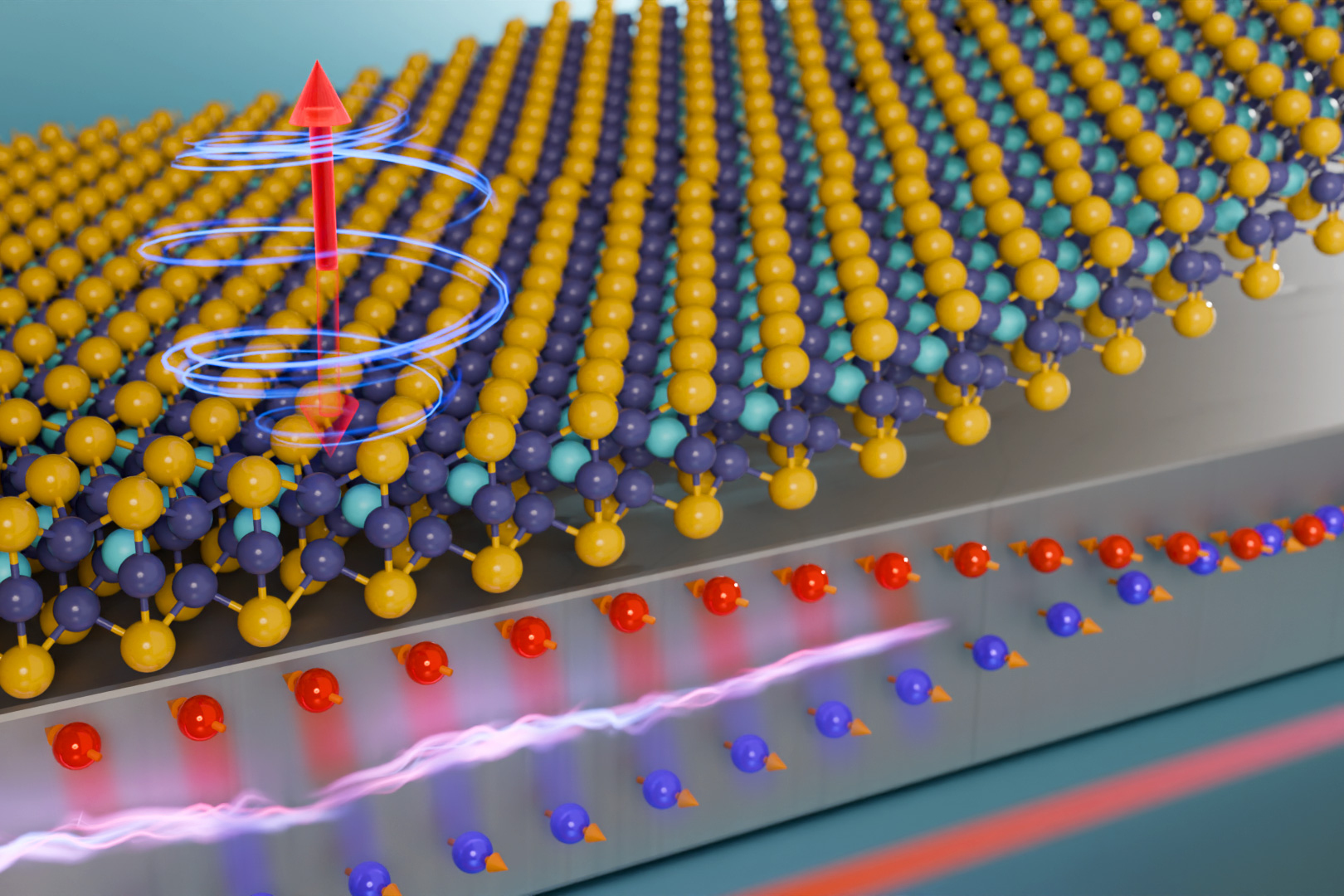
This illustration shows electric current being pumped into platinum (the bottom slab), which results in the creation of an electron spin current that switches the magnetic state of the 2D ferromagnet on top. The colored spheres represent the atoms in the 2D material.
  • ✇MIT News - Nanoscience and nanotechnology | MIT.nano
  • Propelling atomically layered magnets toward green computersMedia Lab
    Globally, computation is booming at an unprecedented rate, fueled by the boons of artificial intelligence. With this, the staggering energy demand of the world’s computing infrastructure has become a major concern, and the development of computing devices that are far more energy-efficient is a leading challenge for the scientific community.  Use of magnetic materials to build computing devices like memories and processors has emerged as a promising avenue for creating “beyond-CMOS” computers,
     

Propelling atomically layered magnets toward green computers

Globally, computation is booming at an unprecedented rate, fueled by the boons of artificial intelligence. With this, the staggering energy demand of the world’s computing infrastructure has become a major concern, and the development of computing devices that are far more energy-efficient is a leading challenge for the scientific community. 

Use of magnetic materials to build computing devices like memories and processors has emerged as a promising avenue for creating “beyond-CMOS” computers, which would use far less energy compared to traditional computers. Magnetization switching in magnets can be used in computation the same way that a transistor switches from open or closed to represent the 0s and 1s of binary code. 

While much of the research along this direction has focused on using bulk magnetic materials, a new class of magnetic materials — called two-dimensional van der Waals magnets — provides superior properties that can improve the scalability and energy efficiency of magnetic devices to make them commercially viable. 

Although the benefits of shifting to 2D magnetic materials are evident, their practical induction into computers has been hindered by some fundamental challenges. Until recently, 2D magnetic materials could operate only at very low temperatures, much like superconductors. So bringing their operating temperatures above room temperature has remained a primary goal. Additionally, for use in computers, it is important that they can be controlled electrically, without the need for magnetic fields. Bridging this fundamental gap, where 2D magnetic materials can be electrically switched above room temperature without any magnetic fields, could potentially catapult the translation of 2D magnets into the next generation of “green” computers.

A team of MIT researchers has now achieved this critical milestone by designing a “van der Waals atomically layered heterostructure” device where a 2D van der Waals magnet, iron gallium telluride, is interfaced with another 2D material, tungsten ditelluride. In an open-access paper published March 15 in Science Advances, the team shows that the magnet can be toggled between the 0 and 1 states simply by applying pulses of electrical current across their two-layer device. 

“Our device enables robust magnetization switching without the need for an external magnetic field, opening up unprecedented opportunities for ultra-low power and environmentally sustainable computing technology for big data and AI,” says lead author Deblina Sarkar, the AT&T Career Development Assistant Professor at the MIT Media Lab and Center for Neurobiological Engineering, and head of the Nano-Cybernetic Biotrek research group. “Moreover, the atomically layered structure of our device provides unique capabilities including improved interface and possibilities of gate voltage tunability, as well as flexible and transparent spintronic technologies.”

Sarkar is joined on the paper by first author Shivam Kajale, a graduate student in Sarkar’s research group at the Media Lab; Thanh Nguyen, a graduate student in the Department of Nuclear Science and Engineering (NSE); Nguyen Tuan Hung, an MIT visiting scholar in NSE and an assistant professor at Tohoku University in Japan; and Mingda Li, associate professor of NSE.

Breaking the mirror symmetries 

When electric current flows through heavy metals like platinum or tantalum, the electrons get segregated in the materials based on their spin component, a phenomenon called the spin Hall effect, says Kajale. The way this segregation happens depends on the material, and particularly its symmetries.

“The conversion of electric current to spin currents in heavy metals lies at the heart of controlling magnets electrically,” Kajale notes. “The microscopic structure of conventionally used materials, like platinum, have a kind of mirror symmetry, which restricts the spin currents only to in-plane spin polarization.”

Kajale explains that two mirror symmetries must be broken to produce an “out-of-plane” spin component that can be transferred to a magnetic layer to induce field-free switching. “Electrical current can 'break' the mirror symmetry along one plane in platinum, but its crystal structure prevents the mirror symmetry from being broken in a second plane.”

In their earlier experiments, the researchers used a small magnetic field to break the second mirror plane. To get rid of the need for a magnetic nudge, Kajale and Sarkar and colleagues looked instead for a material with a structure that could break the second mirror plane without outside help. This led them to another 2D material, tungsten ditelluride. The tungsten ditelluride that the researchers used has an orthorhombic crystal structure. The material itself has one broken mirror plane. Thus, by applying current along its low-symmetry axis (parallel to the broken mirror plane), the resulting spin current has an out-of-plane spin component that can directly induce switching in the ultra-thin magnet interfaced with the tungsten ditelluride. 

“Because it's also a 2D van der Waals material, it can also ensure that when we stack the two materials together, we get pristine interfaces and a good flow of electron spins between the materials,” says Kajale. 

Becoming more energy-efficient 

Computer memory and processors built from magnetic materials use less energy than traditional silicon-based devices. And the van der Waals magnets can offer higher energy efficiency and better scalability compared to bulk magnetic material, the researchers note. 

The electrical current density used for switching the magnet translates to how much energy is dissipated during switching. A lower density means a much more energy-efficient material. “The new design has one of the lowest current densities in van der Waals magnetic materials,” Kajale says. “This new design has an order of magnitude lower in terms of the switching current required in bulk materials. This translates to something like two orders of magnitude improvement in energy efficiency.”

The research team is now looking at similar low-symmetry van der Waals materials to see if they can reduce current density even further. They are also hoping to collaborate with other researchers to find ways to manufacture the 2D magnetic switch devices at commercial scale. 

This work was carried out, in part, using the facilities at MIT.nano. It was funded by the Media Lab, the U.S. National Science Foundation, and the U.S. Department of Energy.

© Image courtesy of the researchers.

The flow of electrical current in the bottom crystalline slab (representing WTe2) breaks a mirror symmetry (shattered glass), while the material itself breaks the other mirror symmetry (cracked glass). The resulting spin current has vertical polarization that switches the magnetic state of the top 2D ferromagnet.

Creative collisions: Crossing the art-science divide

MIT has a rich history of productive collaboration between the arts and the sciences, anchored by the conviction that these two conventionally opposed ways of thinking can form a deeply generative symbiosis that serves to advance and humanize new technologies. 

This ethos was made tangible when the Bauhaus artist and educator György Kepes established the MIT Center for Advanced Visual Studies (CAVS) within the Department of Architecture in 1967. CAVS has since evolved into the Art, Culture, and Technology (ACT) program, which fosters close links to multiple other programs, centers, and labs at MIT. Class 4.373/4.374 (Creating Art, Thinking Science), open to undergraduates and master’s students of all disciplines as well as certain students from the Harvard Graduate School of Design (GSD), is one of the program’s most innovative offerings, proposing a model for how the relationship between art and science might play out at a time of exponential technological growth. 

Now in its third year, the class is supported by an Interdisciplinary Class Development Grant from the MIT Center for Art, Science and Technology (CAST) and draws upon the unparalleled resources of MIT.nano; an artist’s high-tech toolbox for investigating the hidden structures and beauty of our material universe.

High ambitions and critical thinking

The class was initiated by Tobias Putrih, lecturer in ACT, and is taught with the assistance of Ardalan SadeghiKivi MArch ’23, and Aubrie James SM ’24. Central to the success of the class has been the collaboration with co-instructor Vladimir Bulović, the founding director of MIT.nano and Fariborz Maseeh Chair in Emerging Technology, who has positioned the facility as an open-access resource for the campus at large — including MIT’s community of artists. “Creating Art, Thinking Science” unfolds the 100,000 square feet of cleanroom and lab space within the Lisa T. Su Building, inviting participating students to take advantage of cutting-edge equipment for nanoscale visualization and fabrication; in the hands of artists, devices for discovering nanostructures and manipulating atoms become tools for rendering the invisible visible and deconstructing the dynamics of perception itself. 

The expansive goals of the class are tempered by an in-built criticality. “ACT has a unique position as an art program nested within a huge scientific institute — and the challenges of that partnership should not be underestimated,” reflects Putrih. “Science and art are wholly different knowledge systems with distinct historical perspectives. So, how do we communicate? How do we locate that middle ground, that third space?”

An evolving answer, tested and developed throughout the partnership between ACT and MIT.nano, involves a combination of attentive mentorship and sharing of artistic ideas, combined with access to advanced technological resources and hands-on practical training. 

“MIT.nano currently accommodates more than 1,200 individuals to do their work, across 250 different research groups,” says Bulović. “The fact that we count artists among those is a matter of pride for us. We’ve found that the work of our scientists and technologists is enhanced by having access to the language of art as a form of expression — equally, the way that artists express themselves can be stretched beyond what could previously be imagined, simply by having access to the tools and instruments at MIT.nano.”

A playground for experimentation

True to the spirit of the scientific method and artistic iteration, the class is envisioned as a work in progress — a series of propositions and prototypes for how dialogue between scientists and artists might work in practice. The outcomes of those experiments can now be seen installed in the first and second floor galleries at MIT.nano. As part of the facility’s five-year anniversary celebration, the class premiered an exhibition showcasing works created during previous years of “Creating Art, Thinking Science.” 

Visitors to the exhibition, “zero.zerozerozerozerozerozerozerozeroone” (named for the numerical notation for one nanometer), will encounter artworks ranging from a minimalist silicon wafer produced with two-photon polymerization (2PP) technology (“Obscured Invisibility,” 2021, Hyun Woo Park), to traces of an attempt to make vegetable soup in the cleanroom using equipment such as a cryostat, a fluorescing microscope, and a Micro-CT scanner (“May I Please Make You Some Soup?,” 2022, Simone Lasser). 

These works set a precedent for the artworks produced during the fall 2023 iteration of the class. For Ryan Yang, in his senior year studying electrical engineering and computer science at MIT, the chance to engage in open discussion and experimental making has been a rare opportunity to “try something that might not work.” His project explores the possibilities of translating traditional block printing techniques to micron-scale 3D-printing in the MIT.nano labs.

Yang has taken advantage of the arts curriculum at MIT at an early stage in his academic career as an engineer; meanwhile, Ameen Kaleem started out as a filmmaker in New Delhi and is now pursuing a master’s degree in design engineering at Harvard GSD, cross-registered at MIT. 

Kaleem’s project models the process of abiogenesis (the evolution of living organisms from inorganic or inanimate substances) by bringing living moss into the MIT.nano cleanroom facilities to be examined at an atomic scale. “I was interested in the idea that, as a human being in the cleanroom, you are both the most sanitized version of yourself and the dirtiest thing in that space,” she reflects. “Drawing attention to the presence of organic life in the cleanroom is comparable to bringing art into spaces where it might not otherwise exist — a way of humanizing scientific and technological endeavors.”

Consciousness, immersion, and innovation

The students draw upon the legacies of landmark art-science initiatives — including international exhibitions such as “Cybernetic Serendipity” (London ICA, 1968), the “New Tendencies” series (Zagreb, 1961-73), and “Laboratorium” (Antwerp, 1999) — and take inspiration from the instructors’ own creative investigations of the inner workings of different knowledge systems. “In contemporary life, and at MIT in particular, we’re immersed in technology,” says Putrih. “It’s the nature of art to reveal that to us, so that we might see the implications of what we are producing and its potential impact.”

By fostering a mindset of imagination and criticality, combined with building the technical skills to address practical problems, “Creating Art, Thinking Science” seeks to create the conditions for a more expansive version of technological optimism; a culture of innovation in which social and environmental responsibility are seen as productive parameters for enriched creativity. The ripple effects of the class might be years in the making, but as Bulović observes while navigating the exhibition at MIT.nano, “The joy of the collaboration can be felt in the artworks.”

© Photo courtesy of MIT CAST.

Two students engage with an artwork created in 4.373/4.374 (Creating Art, Thinking Science).

Researchers harness 2D magnetic materials for energy-efficient computing

Experimental computer memories and processors built from magnetic materials use far less energy than traditional silicon-based devices. Two-dimensional magnetic materials, composed of layers that are only a few atoms thick, have incredible properties that could allow magnetic-based devices to achieve unprecedented speed, efficiency, and scalability.

While many hurdles must be overcome until these so-called van der Waals magnetic materials can be integrated into functioning computers, MIT researchers took an important step in this direction by demonstrating precise control of a van der Waals magnet at room temperature.

This is key, since magnets composed of atomically thin van der Waals materials can typically only be controlled at extremely cold temperatures, making them difficult to deploy outside a laboratory.

The researchers used pulses of electrical current to switch the direction of the device’s magnetization at room temperature. Magnetic switching can be used in computation, the same way a transistor switches between open and closed to represent 0s and 1s in binary code, or in computer memory, where switching enables data storage.

The team fired bursts of electrons at a magnet made of a new material that can sustain its magnetism at higher temperatures. The experiment leveraged a fundamental property of electrons known as spin, which makes the electrons behave like tiny magnets. By manipulating the spin of electrons that strike the device, the researchers can switch its magnetization.

“The heterostructure device we have developed requires an order of magnitude lower electrical current to switch the van der Waals magnet, compared to that required for bulk magnetic devices,” says Deblina Sarkar, the AT&T Career Development Assistant Professor in the MIT Media Lab and Center for Neurobiological Engineering, head of the Nano-Cybernetic Biotrek Lab, and the senior author of a paper on this technique. “Our device is also more energy efficient than other van der Waals magnets that are unable to switch at room temperature.”

In the future, such a magnet could be used to build faster computers that consume less electricity. It could also enable magnetic computer memories that are nonvolatile, which means they don’t leak information when powered off, or processors that make complex AI algorithms more energy-efficient.

“There is a lot of inertia around trying to improve materials that worked well in the past. But we have shown that if you make radical changes, starting by rethinking the materials you are using, you can potentially get much better solutions,” says Shivam Kajale, a graduate student in Sarkar’s lab and co-lead author of the paper.

Kajale and Sarkar are joined on the paper by co-lead author Thanh Nguyen, a graduate student in the Department of Nuclear Science and Engineering (NSE); Corson Chao, a graduate student in the Department of Materials Science and Engineering (DSME); David Bono, a DSME research scientist; Artittaya Boonkird, an NSE graduate student; and Mingda Li, associate professor of nuclear science and engineering. The research appears this week in Nature Communications.

An atomically thin advantage

Methods to fabricate tiny computer chips in a clean room from bulk materials like silicon can hamper devices. For instance, the layers of material may be barely 1 nanometer thick, so minuscule rough spots on the surface can be severe enough to degrade performance.

By contrast, van der Waals magnetic materials are intrinsically layered and structured in such a way that the surface remains perfectly smooth, even as researchers peel off layers to make thinner devices. In addition, atoms in one layer won’t leak into other layers, enabling the materials to retain their unique properties when stacked in devices.

“In terms of scaling and making these magnetic devices competitive for commercial applications, van der Waals materials are the way to go,” Kajale says.

But there’s a catch. This new class of magnetic materials have typically only been operated at temperatures below 60 kelvins (-351 degrees Fahrenheit). To build a magnetic computer processor or memory, researchers need to use electrical current to operate the magnet at room temperature.

To achieve this, the team focused on an emerging material called iron gallium telluride. This atomically thin material has all the properties needed for effective room temperature magnetism and doesn’t contain rare earth elements, which are undesirable because extracting them is especially destructive to the environment.

Nguyen carefully grew bulk crystals of this 2D material using a special technique. Then, Kajale fabricated a two-layer magnetic device using nanoscale flakes of iron gallium telluride underneath a six-nanometer layer of platinum.

Tiny device in hand, they used an intrinsic property of electrons known as spin to switch its magnetization at room temperature.

Electron ping-pong

While electrons don’t technically “spin” like a top, they do possess the same kind of angular momentum. That spin has a direction, either up or down. The researchers can leverage a property known as spin-orbit coupling to control the spins of electrons they fire at the magnet.

The same way momentum is transferred when one ball hits another, electrons will transfer their “spin momentum” to the 2D magnetic material when they strike it. Depending on the direction of their spins, that momentum transfer can reverse the magnetization.

In a sense, this transfer rotates the magnetization from up to down (or vice-versa), so it is called a “torque,” as in spin-orbit torque switching. Applying a negative electric pulse causes the magnetization to go downward, while a positive pulse causes it to go upward.

The researchers can do this switching at room temperature for two reasons: the special properties of iron gallium telluride and the fact that their technique uses small amounts of electrical current. Pumping too much current into the device would cause it to overheat and demagnetize.

The team faced many challenges over the two years it took to achieve this milestone, Kajale says. Finding the right magnetic material was only half the battle. Since iron gallium telluride oxidizes quickly, fabrication must be done inside a glovebox filled with nitrogen.

“The device is only exposed to air for 10 or 15 seconds, but even after that I have to do a step where I polish it to remove any oxide,” he says.

Now that they have demonstrated room-temperature switching and greater energy efficiency, the researchers plan to keep pushing the performance of magnetic van der Waals materials.

“Our next milestone is to achieve switching without the need for any external magnetic fields. Our aim is to enhance our technology and scale up to bring the versatility of van der Waals magnet to commercial applications,” Sarkar says.

This work was carried out, in part, using the facilities at MIT.Nano and the Harvard University Center for Nanoscale Systems.

© Image: Courtesy of the researchers

This illustration shows electric current being pumped into platinum (the bottom slab), which results in the creation of an electron spin current that switches the magnetic state of the 2D ferromagnet on top. The colored spheres represent the atoms in the 2D material.
  • ✇MIT News - Nanoscience and nanotechnology | MIT.nano
  • Propelling atomically layered magnets toward green computersMedia Lab
    Globally, computation is booming at an unprecedented rate, fueled by the boons of artificial intelligence. With this, the staggering energy demand of the world’s computing infrastructure has become a major concern, and the development of computing devices that are far more energy-efficient is a leading challenge for the scientific community.  Use of magnetic materials to build computing devices like memories and processors has emerged as a promising avenue for creating “beyond-CMOS” computers,
     

Propelling atomically layered magnets toward green computers

Globally, computation is booming at an unprecedented rate, fueled by the boons of artificial intelligence. With this, the staggering energy demand of the world’s computing infrastructure has become a major concern, and the development of computing devices that are far more energy-efficient is a leading challenge for the scientific community. 

Use of magnetic materials to build computing devices like memories and processors has emerged as a promising avenue for creating “beyond-CMOS” computers, which would use far less energy compared to traditional computers. Magnetization switching in magnets can be used in computation the same way that a transistor switches from open or closed to represent the 0s and 1s of binary code. 

While much of the research along this direction has focused on using bulk magnetic materials, a new class of magnetic materials — called two-dimensional van der Waals magnets — provides superior properties that can improve the scalability and energy efficiency of magnetic devices to make them commercially viable. 

Although the benefits of shifting to 2D magnetic materials are evident, their practical induction into computers has been hindered by some fundamental challenges. Until recently, 2D magnetic materials could operate only at very low temperatures, much like superconductors. So bringing their operating temperatures above room temperature has remained a primary goal. Additionally, for use in computers, it is important that they can be controlled electrically, without the need for magnetic fields. Bridging this fundamental gap, where 2D magnetic materials can be electrically switched above room temperature without any magnetic fields, could potentially catapult the translation of 2D magnets into the next generation of “green” computers.

A team of MIT researchers has now achieved this critical milestone by designing a “van der Waals atomically layered heterostructure” device where a 2D van der Waals magnet, iron gallium telluride, is interfaced with another 2D material, tungsten ditelluride. In an open-access paper published March 15 in Science Advances, the team shows that the magnet can be toggled between the 0 and 1 states simply by applying pulses of electrical current across their two-layer device. 

“Our device enables robust magnetization switching without the need for an external magnetic field, opening up unprecedented opportunities for ultra-low power and environmentally sustainable computing technology for big data and AI,” says lead author Deblina Sarkar, the AT&T Career Development Assistant Professor at the MIT Media Lab and Center for Neurobiological Engineering, and head of the Nano-Cybernetic Biotrek research group. “Moreover, the atomically layered structure of our device provides unique capabilities including improved interface and possibilities of gate voltage tunability, as well as flexible and transparent spintronic technologies.”

Sarkar is joined on the paper by first author Shivam Kajale, a graduate student in Sarkar’s research group at the Media Lab; Thanh Nguyen, a graduate student in the Department of Nuclear Science and Engineering (NSE); Nguyen Tuan Hung, an MIT visiting scholar in NSE and an assistant professor at Tohoku University in Japan; and Mingda Li, associate professor of NSE.

Breaking the mirror symmetries 

When electric current flows through heavy metals like platinum or tantalum, the electrons get segregated in the materials based on their spin component, a phenomenon called the spin Hall effect, says Kajale. The way this segregation happens depends on the material, and particularly its symmetries.

“The conversion of electric current to spin currents in heavy metals lies at the heart of controlling magnets electrically,” Kajale notes. “The microscopic structure of conventionally used materials, like platinum, have a kind of mirror symmetry, which restricts the spin currents only to in-plane spin polarization.”

Kajale explains that two mirror symmetries must be broken to produce an “out-of-plane” spin component that can be transferred to a magnetic layer to induce field-free switching. “Electrical current can 'break' the mirror symmetry along one plane in platinum, but its crystal structure prevents the mirror symmetry from being broken in a second plane.”

In their earlier experiments, the researchers used a small magnetic field to break the second mirror plane. To get rid of the need for a magnetic nudge, Kajale and Sarkar and colleagues looked instead for a material with a structure that could break the second mirror plane without outside help. This led them to another 2D material, tungsten ditelluride. The tungsten ditelluride that the researchers used has an orthorhombic crystal structure. The material itself has one broken mirror plane. Thus, by applying current along its low-symmetry axis (parallel to the broken mirror plane), the resulting spin current has an out-of-plane spin component that can directly induce switching in the ultra-thin magnet interfaced with the tungsten ditelluride. 

“Because it's also a 2D van der Waals material, it can also ensure that when we stack the two materials together, we get pristine interfaces and a good flow of electron spins between the materials,” says Kajale. 

Becoming more energy-efficient 

Computer memory and processors built from magnetic materials use less energy than traditional silicon-based devices. And the van der Waals magnets can offer higher energy efficiency and better scalability compared to bulk magnetic material, the researchers note. 

The electrical current density used for switching the magnet translates to how much energy is dissipated during switching. A lower density means a much more energy-efficient material. “The new design has one of the lowest current densities in van der Waals magnetic materials,” Kajale says. “This new design has an order of magnitude lower in terms of the switching current required in bulk materials. This translates to something like two orders of magnitude improvement in energy efficiency.”

The research team is now looking at similar low-symmetry van der Waals materials to see if they can reduce current density even further. They are also hoping to collaborate with other researchers to find ways to manufacture the 2D magnetic switch devices at commercial scale. 

This work was carried out, in part, using the facilities at MIT.nano. It was funded by the Media Lab, the U.S. National Science Foundation, and the U.S. Department of Energy.

© Image courtesy of the researchers.
The flow of electrical current in the bottom crystalline slab (representing WTe2) breaks a mirror symmetry (shattered glass), while the material itself breaks the other mirror symmetry (cracked glass). The resulting spin current has vertical polarization that switches the magnetic state of the top 2D ferromagnet.

Creative collisions: Crossing the art-science divide

MIT has a rich history of productive collaboration between the arts and the sciences, anchored by the conviction that these two conventionally opposed ways of thinking can form a deeply generative symbiosis that serves to advance and humanize new technologies. 

This ethos was made tangible when the Bauhaus artist and educator György Kepes established the MIT Center for Advanced Visual Studies (CAVS) within the Department of Architecture in 1967. CAVS has since evolved into the Art, Culture, and Technology (ACT) program, which fosters close links to multiple other programs, centers, and labs at MIT. Class 4.373/4.374 (Creating Art, Thinking Science), open to undergraduates and master’s students of all disciplines as well as certain students from the Harvard Graduate School of Design (GSD), is one of the program’s most innovative offerings, proposing a model for how the relationship between art and science might play out at a time of exponential technological growth. 

Now in its third year, the class is supported by an Interdisciplinary Class Development Grant from the MIT Center for Art, Science and Technology (CAST) and draws upon the unparalleled resources of MIT.nano; an artist’s high-tech toolbox for investigating the hidden structures and beauty of our material universe.

High ambitions and critical thinking

The class was initiated by Tobias Putrih, lecturer in ACT, and is taught with the assistance of Ardalan SadeghiKivi MArch ’23, and Aubrie James SM ’24. Central to the success of the class has been the collaboration with co-instructor Vladimir Bulović, the founding director of MIT.nano and Fariborz Maseeh Chair in Emerging Technology, who has positioned the facility as an open-access resource for the campus at large — including MIT’s community of artists. “Creating Art, Thinking Science” unfolds the 100,000 square feet of cleanroom and lab space within the Lisa T. Su Building, inviting participating students to take advantage of cutting-edge equipment for nanoscale visualization and fabrication; in the hands of artists, devices for discovering nanostructures and manipulating atoms become tools for rendering the invisible visible and deconstructing the dynamics of perception itself. 

The expansive goals of the class are tempered by an in-built criticality. “ACT has a unique position as an art program nested within a huge scientific institute — and the challenges of that partnership should not be underestimated,” reflects Putrih. “Science and art are wholly different knowledge systems with distinct historical perspectives. So, how do we communicate? How do we locate that middle ground, that third space?”

An evolving answer, tested and developed throughout the partnership between ACT and MIT.nano, involves a combination of attentive mentorship and sharing of artistic ideas, combined with access to advanced technological resources and hands-on practical training. 

“MIT.nano currently accommodates more than 1,200 individuals to do their work, across 250 different research groups,” says Bulović. “The fact that we count artists among those is a matter of pride for us. We’ve found that the work of our scientists and technologists is enhanced by having access to the language of art as a form of expression — equally, the way that artists express themselves can be stretched beyond what could previously be imagined, simply by having access to the tools and instruments at MIT.nano.”

A playground for experimentation

True to the spirit of the scientific method and artistic iteration, the class is envisioned as a work in progress — a series of propositions and prototypes for how dialogue between scientists and artists might work in practice. The outcomes of those experiments can now be seen installed in the first and second floor galleries at MIT.nano. As part of the facility’s five-year anniversary celebration, the class premiered an exhibition showcasing works created during previous years of “Creating Art, Thinking Science.” 

Visitors to the exhibition, “zero.zerozerozerozerozerozerozerozeroone” (named for the numerical notation for one nanometer), will encounter artworks ranging from a minimalist silicon wafer produced with two-photon polymerization (2PP) technology (“Obscured Invisibility,” 2021, Hyun Woo Park), to traces of an attempt to make vegetable soup in the cleanroom using equipment such as a cryostat, a fluorescing microscope, and a Micro-CT scanner (“May I Please Make You Some Soup?,” 2022, Simone Lasser). 

These works set a precedent for the artworks produced during the fall 2023 iteration of the class. For Ryan Yang, in his senior year studying electrical engineering and computer science at MIT, the chance to engage in open discussion and experimental making has been a rare opportunity to “try something that might not work.” His project explores the possibilities of translating traditional block printing techniques to micron-scale 3D-printing in the MIT.nano labs.

Yang has taken advantage of the arts curriculum at MIT at an early stage in his academic career as an engineer; meanwhile, Ameen Kaleem started out as a filmmaker in New Delhi and is now pursuing a master’s degree in design engineering at Harvard GSD, cross-registered at MIT. 

Kaleem’s project models the process of abiogenesis (the evolution of living organisms from inorganic or inanimate substances) by bringing living moss into the MIT.nano cleanroom facilities to be examined at an atomic scale. “I was interested in the idea that, as a human being in the cleanroom, you are both the most sanitized version of yourself and the dirtiest thing in that space,” she reflects. “Drawing attention to the presence of organic life in the cleanroom is comparable to bringing art into spaces where it might not otherwise exist — a way of humanizing scientific and technological endeavors.”

Consciousness, immersion, and innovation

The students draw upon the legacies of landmark art-science initiatives — including international exhibitions such as “Cybernetic Serendipity” (London ICA, 1968), the “New Tendencies” series (Zagreb, 1961-73), and “Laboratorium” (Antwerp, 1999) — and take inspiration from the instructors’ own creative investigations of the inner workings of different knowledge systems. “In contemporary life, and at MIT in particular, we’re immersed in technology,” says Putrih. “It’s the nature of art to reveal that to us, so that we might see the implications of what we are producing and its potential impact.”

By fostering a mindset of imagination and criticality, combined with building the technical skills to address practical problems, “Creating Art, Thinking Science” seeks to create the conditions for a more expansive version of technological optimism; a culture of innovation in which social and environmental responsibility are seen as productive parameters for enriched creativity. The ripple effects of the class might be years in the making, but as Bulović observes while navigating the exhibition at MIT.nano, “The joy of the collaboration can be felt in the artworks.”

© Photo courtesy of MIT CAST.

Two students engage with an artwork created in 4.373/4.374 (Creating Art, Thinking Science).

Researchers harness 2D magnetic materials for energy-efficient computing

Experimental computer memories and processors built from magnetic materials use far less energy than traditional silicon-based devices. Two-dimensional magnetic materials, composed of layers that are only a few atoms thick, have incredible properties that could allow magnetic-based devices to achieve unprecedented speed, efficiency, and scalability.

While many hurdles must be overcome until these so-called van der Waals magnetic materials can be integrated into functioning computers, MIT researchers took an important step in this direction by demonstrating precise control of a van der Waals magnet at room temperature.

This is key, since magnets composed of atomically thin van der Waals materials can typically only be controlled at extremely cold temperatures, making them difficult to deploy outside a laboratory.

The researchers used pulses of electrical current to switch the direction of the device’s magnetization at room temperature. Magnetic switching can be used in computation, the same way a transistor switches between open and closed to represent 0s and 1s in binary code, or in computer memory, where switching enables data storage.

The team fired bursts of electrons at a magnet made of a new material that can sustain its magnetism at higher temperatures. The experiment leveraged a fundamental property of electrons known as spin, which makes the electrons behave like tiny magnets. By manipulating the spin of electrons that strike the device, the researchers can switch its magnetization.

“The heterostructure device we have developed requires an order of magnitude lower electrical current to switch the van der Waals magnet, compared to that required for bulk magnetic devices,” says Deblina Sarkar, the AT&T Career Development Assistant Professor in the MIT Media Lab and Center for Neurobiological Engineering, head of the Nano-Cybernetic Biotrek Lab, and the senior author of a paper on this technique. “Our device is also more energy efficient than other van der Waals magnets that are unable to switch at room temperature.”

In the future, such a magnet could be used to build faster computers that consume less electricity. It could also enable magnetic computer memories that are nonvolatile, which means they don’t leak information when powered off, or processors that make complex AI algorithms more energy-efficient.

“There is a lot of inertia around trying to improve materials that worked well in the past. But we have shown that if you make radical changes, starting by rethinking the materials you are using, you can potentially get much better solutions,” says Shivam Kajale, a graduate student in Sarkar’s lab and co-lead author of the paper.

Kajale and Sarkar are joined on the paper by co-lead author Thanh Nguyen, a graduate student in the Department of Nuclear Science and Engineering (NSE); Corson Chao, a graduate student in the Department of Materials Science and Engineering (DSME); David Bono, a DSME research scientist; Artittaya Boonkird, an NSE graduate student; and Mingda Li, associate professor of nuclear science and engineering. The research appears this week in Nature Communications.

An atomically thin advantage

Methods to fabricate tiny computer chips in a clean room from bulk materials like silicon can hamper devices. For instance, the layers of material may be barely 1 nanometer thick, so minuscule rough spots on the surface can be severe enough to degrade performance.

By contrast, van der Waals magnetic materials are intrinsically layered and structured in such a way that the surface remains perfectly smooth, even as researchers peel off layers to make thinner devices. In addition, atoms in one layer won’t leak into other layers, enabling the materials to retain their unique properties when stacked in devices.

“In terms of scaling and making these magnetic devices competitive for commercial applications, van der Waals materials are the way to go,” Kajale says.

But there’s a catch. This new class of magnetic materials have typically only been operated at temperatures below 60 kelvins (-351 degrees Fahrenheit). To build a magnetic computer processor or memory, researchers need to use electrical current to operate the magnet at room temperature.

To achieve this, the team focused on an emerging material called iron gallium telluride. This atomically thin material has all the properties needed for effective room temperature magnetism and doesn’t contain rare earth elements, which are undesirable because extracting them is especially destructive to the environment.

Nguyen carefully grew bulk crystals of this 2D material using a special technique. Then, Kajale fabricated a two-layer magnetic device using nanoscale flakes of iron gallium telluride underneath a six-nanometer layer of platinum.

Tiny device in hand, they used an intrinsic property of electrons known as spin to switch its magnetization at room temperature.

Electron ping-pong

While electrons don’t technically “spin” like a top, they do possess the same kind of angular momentum. That spin has a direction, either up or down. The researchers can leverage a property known as spin-orbit coupling to control the spins of electrons they fire at the magnet.

The same way momentum is transferred when one ball hits another, electrons will transfer their “spin momentum” to the 2D magnetic material when they strike it. Depending on the direction of their spins, that momentum transfer can reverse the magnetization.

In a sense, this transfer rotates the magnetization from up to down (or vice-versa), so it is called a “torque,” as in spin-orbit torque switching. Applying a negative electric pulse causes the magnetization to go downward, while a positive pulse causes it to go upward.

The researchers can do this switching at room temperature for two reasons: the special properties of iron gallium telluride and the fact that their technique uses small amounts of electrical current. Pumping too much current into the device would cause it to overheat and demagnetize.

The team faced many challenges over the two years it took to achieve this milestone, Kajale says. Finding the right magnetic material was only half the battle. Since iron gallium telluride oxidizes quickly, fabrication must be done inside a glovebox filled with nitrogen.

“The device is only exposed to air for 10 or 15 seconds, but even after that I have to do a step where I polish it to remove any oxide,” he says.

Now that they have demonstrated room-temperature switching and greater energy efficiency, the researchers plan to keep pushing the performance of magnetic van der Waals materials.

“Our next milestone is to achieve switching without the need for any external magnetic fields. Our aim is to enhance our technology and scale up to bring the versatility of van der Waals magnet to commercial applications,” Sarkar says.

This work was carried out, in part, using the facilities at MIT.Nano and the Harvard University Center for Nanoscale Systems.

© Image: Courtesy of the researchers

This illustration shows electric current being pumped into platinum (the bottom slab), which results in the creation of an electron spin current that switches the magnetic state of the 2D ferromagnet on top. The colored spheres represent the atoms in the 2D material.
❌
❌