Last week ARM unveiled their new IP that will be featured in the devices consumers buy in 2025.Read more ▶
The post ARM Outs Their New IP lineup for 2024 appeared first on SemiAccurate.
MIT has a rich history of productive collaboration between the arts and the sciences, anchored by the conviction that these two conventionally opposed ways of thinking can form a deeply generative symbiosis that serves to advance and humanize new technologies.
This ethos was made tangible when the Bauhaus artist and educator György Kepes established the MIT Center for Advanced Visual Studies (CAVS) within the Department of Architecture in 1967. CAVS has since evolved into the Art, Culture, and
MIT has a rich history of productive collaboration between the arts and the sciences, anchored by the conviction that these two conventionally opposed ways of thinking can form a deeply generative symbiosis that serves to advance and humanize new technologies.
This ethos was made tangible when the Bauhaus artist and educator György Kepes established the MIT Center for Advanced Visual Studies (CAVS) within the Department of Architecture in 1967. CAVS has since evolved into the Art, Culture, and Technology (ACT) program, which fosters close links to multiple other programs, centers, and labs at MIT. Class 4.373/4.374 (Creating Art, Thinking Science), open to undergraduates and master’s students of all disciplines as well as certain students from the Harvard Graduate School of Design (GSD), is one of the program’s most innovative offerings, proposing a model for how the relationship between art and science might play out at a time of exponential technological growth.
Now in its third year, the class is supported by an Interdisciplinary Class Development Grant from the MIT Center for Art, Science and Technology (CAST) and draws upon the unparalleled resources of MIT.nano; an artist’s high-tech toolbox for investigating the hidden structures and beauty of our material universe.
High ambitions and critical thinking
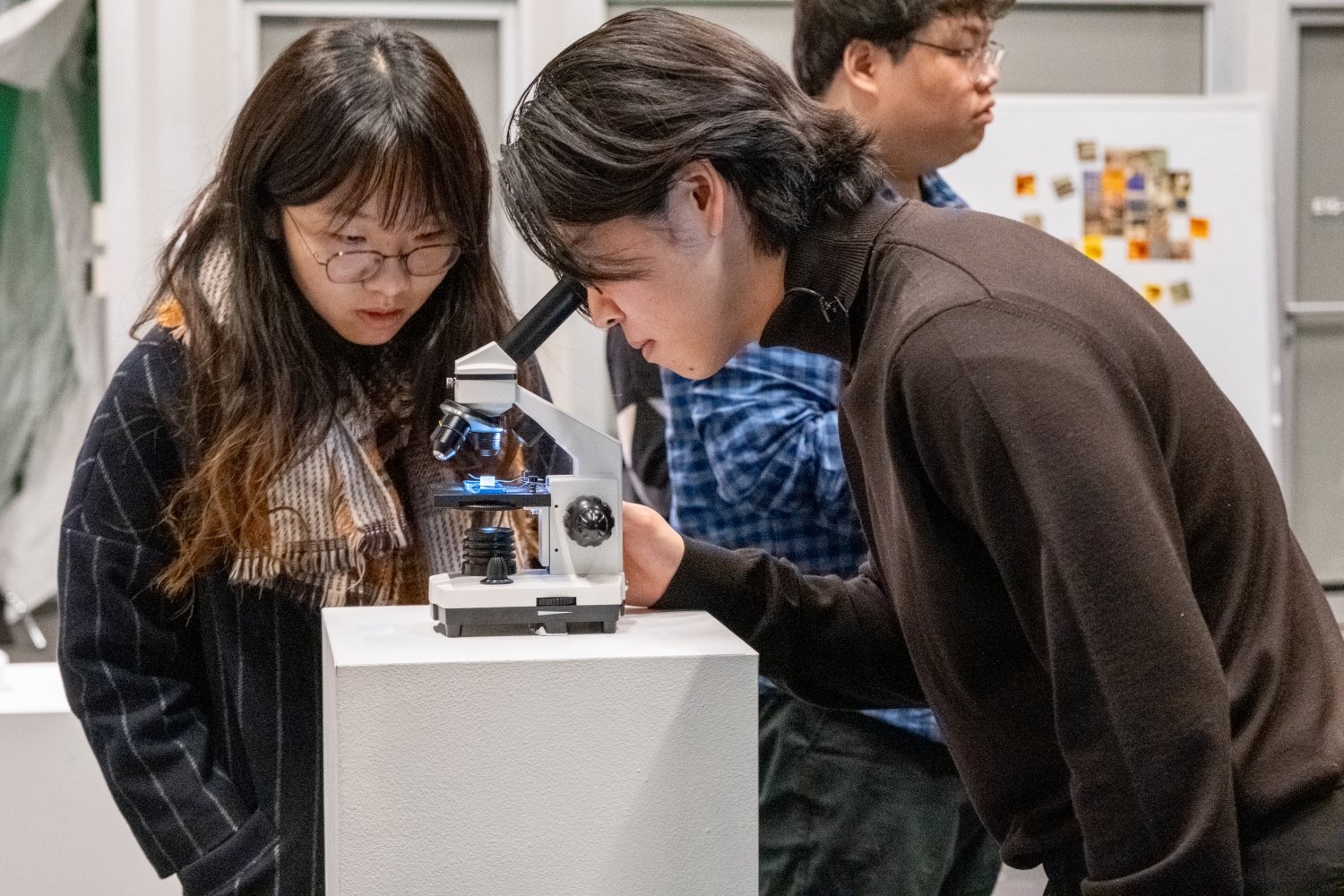
The class was initiated by Tobias Putrih, lecturer in ACT, and is taught with the assistance of Ardalan SadeghiKivi MArch ’23, and Aubrie James SM ’24. Central to the success of the class has been the collaboration with co-instructor Vladimir Bulović, the founding director of MIT.nano and Fariborz Maseeh Chair in Emerging Technology, who has positioned the facility as an open-access resource for the campus at large — including MIT’s community of artists. “Creating Art, Thinking Science” unfolds the 100,000 square feet of cleanroom and lab space within the Lisa T. Su Building, inviting participating students to take advantage of cutting-edge equipment for nanoscale visualization and fabrication; in the hands of artists, devices for discovering nanostructures and manipulating atoms become tools for rendering the invisible visible and deconstructing the dynamics of perception itself.
The expansive goals of the class are tempered by an in-built criticality. “ACT has a unique position as an art program nested within a huge scientific institute — and the challenges of that partnership should not be underestimated,” reflects Putrih. “Science and art are wholly different knowledge systems with distinct historical perspectives. So, how do we communicate? How do we locate that middle ground, that third space?”
An evolving answer, tested and developed throughout the partnership between ACT and MIT.nano, involves a combination of attentive mentorship and sharing of artistic ideas, combined with access to advanced technological resources and hands-on practical training.
“MIT.nano currently accommodates more than 1,200 individuals to do their work, across 250 different research groups,” says Bulović. “The fact that we count artists among those is a matter of pride for us. We’ve found that the work of our scientists and technologists is enhanced by having access to the language of art as a form of expression — equally, the way that artists express themselves can be stretched beyond what could previously be imagined, simply by having access to the tools and instruments at MIT.nano.”
A playground for experimentation
True to the spirit of the scientific method and artistic iteration, the class is envisioned as a work in progress — a series of propositions and prototypes for how dialogue between scientists and artists might work in practice. The outcomes of those experiments can now be seen installed in the first and second floor galleries at MIT.nano. As part of the facility’s five-year anniversary celebration, the class premiered an exhibition showcasing works created during previous years of “Creating Art, Thinking Science.”
Visitors to the exhibition, “zero.zerozerozerozerozerozerozerozeroone” (named for the numerical notation for one nanometer), will encounter artworks ranging from a minimalist silicon wafer produced with two-photon polymerization (2PP) technology (“Obscured Invisibility,” 2021, Hyun Woo Park), to traces of an attempt to make vegetable soup in the cleanroom using equipment such as a cryostat, a fluorescing microscope, and a Micro-CT scanner (“May I Please Make You Some Soup?,” 2022, Simone Lasser).
These works set a precedent for the artworks produced during the fall 2023 iteration of the class. For Ryan Yang, in his senior year studying electrical engineering and computer science at MIT, the chance to engage in open discussion and experimental making has been a rare opportunity to “try something that might not work.” His project explores the possibilities of translating traditional block printing techniques to micron-scale 3D-printing in the MIT.nano labs.
Yang has taken advantage of the arts curriculum at MIT at an early stage in his academic career as an engineer; meanwhile, Ameen Kaleem started out as a filmmaker in New Delhi and is now pursuing a master’s degree in design engineering at Harvard GSD, cross-registered at MIT.
Kaleem’s project models the process of abiogenesis (the evolution of living organisms from inorganic or inanimate substances) by bringing living moss into the MIT.nano cleanroom facilities to be examined at an atomic scale. “I was interested in the idea that, as a human being in the cleanroom, you are both the most sanitized version of yourself and the dirtiest thing in that space,” she reflects. “Drawing attention to the presence of organic life in the cleanroom is comparable to bringing art into spaces where it might not otherwise exist — a way of humanizing scientific and technological endeavors.”
Consciousness, immersion, and innovation
The students draw upon the legacies of landmark art-science initiatives — including international exhibitions such as “Cybernetic Serendipity” (London ICA, 1968), the “New Tendencies” series (Zagreb, 1961-73), and “Laboratorium” (Antwerp, 1999) — and take inspiration from the instructors’ own creative investigations of the inner workings of different knowledge systems. “In contemporary life, and at MIT in particular, we’re immersed in technology,” says Putrih. “It’s the nature of art to reveal that to us, so that we might see the implications of what we are producing and its potential impact.”
By fostering a mindset of imagination and criticality, combined with building the technical skills to address practical problems, “Creating Art, Thinking Science” seeks to create the conditions for a more expansive version of technological optimism; a culture of innovation in which social and environmental responsibility are seen as productive parameters for enriched creativity. The ripple effects of the class might be years in the making, but as Bulović observes while navigating the exhibition at MIT.nano, “The joy of the collaboration can be felt in the artworks.”
MIT has a rich history of productive collaboration between the arts and the sciences, anchored by the conviction that these two conventionally opposed ways of thinking can form a deeply generative symbiosis that serves to advance and humanize new technologies.
This ethos was made tangible when the Bauhaus artist and educator György Kepes established the MIT Center for Advanced Visual Studies (CAVS) within the Department of Architecture in 1967. CAVS has since evolved into the Art, Culture, and
MIT has a rich history of productive collaboration between the arts and the sciences, anchored by the conviction that these two conventionally opposed ways of thinking can form a deeply generative symbiosis that serves to advance and humanize new technologies.
This ethos was made tangible when the Bauhaus artist and educator György Kepes established the MIT Center for Advanced Visual Studies (CAVS) within the Department of Architecture in 1967. CAVS has since evolved into the Art, Culture, and Technology (ACT) program, which fosters close links to multiple other programs, centers, and labs at MIT. Class 4.373/4.374 (Creating Art, Thinking Science), open to undergraduates and master’s students of all disciplines as well as certain students from the Harvard Graduate School of Design (GSD), is one of the program’s most innovative offerings, proposing a model for how the relationship between art and science might play out at a time of exponential technological growth.
Now in its third year, the class is supported by an Interdisciplinary Class Development Grant from the MIT Center for Art, Science and Technology (CAST) and draws upon the unparalleled resources of MIT.nano; an artist’s high-tech toolbox for investigating the hidden structures and beauty of our material universe.
High ambitions and critical thinking
The class was initiated by Tobias Putrih, lecturer in ACT, and is taught with the assistance of Ardalan SadeghiKivi MArch ’23, and Aubrie James SM ’24. Central to the success of the class has been the collaboration with co-instructor Vladimir Bulović, the founding director of MIT.nano and Fariborz Maseeh Chair in Emerging Technology, who has positioned the facility as an open-access resource for the campus at large — including MIT’s community of artists. “Creating Art, Thinking Science” unfolds the 100,000 square feet of cleanroom and lab space within the Lisa T. Su Building, inviting participating students to take advantage of cutting-edge equipment for nanoscale visualization and fabrication; in the hands of artists, devices for discovering nanostructures and manipulating atoms become tools for rendering the invisible visible and deconstructing the dynamics of perception itself.
The expansive goals of the class are tempered by an in-built criticality. “ACT has a unique position as an art program nested within a huge scientific institute — and the challenges of that partnership should not be underestimated,” reflects Putrih. “Science and art are wholly different knowledge systems with distinct historical perspectives. So, how do we communicate? How do we locate that middle ground, that third space?”
An evolving answer, tested and developed throughout the partnership between ACT and MIT.nano, involves a combination of attentive mentorship and sharing of artistic ideas, combined with access to advanced technological resources and hands-on practical training.
“MIT.nano currently accommodates more than 1,200 individuals to do their work, across 250 different research groups,” says Bulović. “The fact that we count artists among those is a matter of pride for us. We’ve found that the work of our scientists and technologists is enhanced by having access to the language of art as a form of expression — equally, the way that artists express themselves can be stretched beyond what could previously be imagined, simply by having access to the tools and instruments at MIT.nano.”
A playground for experimentation
True to the spirit of the scientific method and artistic iteration, the class is envisioned as a work in progress — a series of propositions and prototypes for how dialogue between scientists and artists might work in practice. The outcomes of those experiments can now be seen installed in the first and second floor galleries at MIT.nano. As part of the facility’s five-year anniversary celebration, the class premiered an exhibition showcasing works created during previous years of “Creating Art, Thinking Science.”
Visitors to the exhibition, “zero.zerozerozerozerozerozerozerozeroone” (named for the numerical notation for one nanometer), will encounter artworks ranging from a minimalist silicon wafer produced with two-photon polymerization (2PP) technology (“Obscured Invisibility,” 2021, Hyun Woo Park), to traces of an attempt to make vegetable soup in the cleanroom using equipment such as a cryostat, a fluorescing microscope, and a Micro-CT scanner (“May I Please Make You Some Soup?,” 2022, Simone Lasser).
These works set a precedent for the artworks produced during the fall 2023 iteration of the class. For Ryan Yang, in his senior year studying electrical engineering and computer science at MIT, the chance to engage in open discussion and experimental making has been a rare opportunity to “try something that might not work.” His project explores the possibilities of translating traditional block printing techniques to micron-scale 3D-printing in the MIT.nano labs.
Yang has taken advantage of the arts curriculum at MIT at an early stage in his academic career as an engineer; meanwhile, Ameen Kaleem started out as a filmmaker in New Delhi and is now pursuing a master’s degree in design engineering at Harvard GSD, cross-registered at MIT.
Kaleem’s project models the process of abiogenesis (the evolution of living organisms from inorganic or inanimate substances) by bringing living moss into the MIT.nano cleanroom facilities to be examined at an atomic scale. “I was interested in the idea that, as a human being in the cleanroom, you are both the most sanitized version of yourself and the dirtiest thing in that space,” she reflects. “Drawing attention to the presence of organic life in the cleanroom is comparable to bringing art into spaces where it might not otherwise exist — a way of humanizing scientific and technological endeavors.”
Consciousness, immersion, and innovation
The students draw upon the legacies of landmark art-science initiatives — including international exhibitions such as “Cybernetic Serendipity” (London ICA, 1968), the “New Tendencies” series (Zagreb, 1961-73), and “Laboratorium” (Antwerp, 1999) — and take inspiration from the instructors’ own creative investigations of the inner workings of different knowledge systems. “In contemporary life, and at MIT in particular, we’re immersed in technology,” says Putrih. “It’s the nature of art to reveal that to us, so that we might see the implications of what we are producing and its potential impact.”
By fostering a mindset of imagination and criticality, combined with building the technical skills to address practical problems, “Creating Art, Thinking Science” seeks to create the conditions for a more expansive version of technological optimism; a culture of innovation in which social and environmental responsibility are seen as productive parameters for enriched creativity. The ripple effects of the class might be years in the making, but as Bulović observes while navigating the exhibition at MIT.nano, “The joy of the collaboration can be felt in the artworks.”
In the automotive industry, AI-enabled automotive devices and systems are dramatically transforming the way SoCs are designed, making high-quality and reliable die-to-die and chip-to-chip connectivity non-negotiable. This article explains how interface IP for die-to-die connectivity, display, and storage can support new developments in automotive SoCs for the most advanced innovations such as centralized zonal architecture and integrated ADAS and IVI applications.
AI-integrated ADAS SoCs
The aut
In the automotive industry, AI-enabled automotive devices and systems are dramatically transforming the way SoCs are designed, making high-quality and reliable die-to-die and chip-to-chip connectivity non-negotiable. This article explains how interface IP for die-to-die connectivity, display, and storage can support new developments in automotive SoCs for the most advanced innovations such as centralized zonal architecture and integrated ADAS and IVI applications.
AI-integrated ADAS SoCs
The automotive industry is adopting a new electronic/electric (EE) architecture where a centralized compute module executes multiple applications such as ADAS and in-vehicle infotainment (IVI). With the advent of EVs and more advanced features in the car, the new centralized zonal architecture will help minimize complexity, maximize scalability, and facilitate faster decision-making time. This new architecture is demanding a new set of SoCs on advanced process technologies with very high performance. More traditional monolithic SoCs for single functions like ADAS are giving way to multi-die designs where various dies are connected in a single package and placed in a system to perform a function in the car. While such multi-die designs are gaining adoption, semiconductor companies must remain cost-conscious as these ADAS SoCs will be manufactured at high volumes for a myriad of safety levels. One example is the automated driving central compute system. The system can include modules for the sensor interface, safety management, memory control and interfaces, and dies for CPU, GPU, and AI accelerator, which are then connected via a die-to-die interface such as the Universal Chiplet Interconnect Express (UCIe). Figure 1 illustrates how semiconductor companies can develop SoCs for such systems using multi-die designs. For a base ADAS or IVI SoC, the requirement might just be the CPU die for a level 2 functional safety. A GPU die can be added to the base CPU die for a base ADAS or premium IVI function at a level 2+ driving automation. To allow more compute power for AI workloads, an NPU die can be added to the base CPU or the base CPU and GPU dies for level 3/3+ functional safety. None of these scalable scenarios are possible without a solution for die-to-die connectivity.
Fig. 1: A simplified view of automotive systems using multi-die designs.
The adoption of UCIe for automotive SoCs
The industry has come together to define, develop, and deploy the UCIe standard, a universal interconnect at the package-level. In a recent news release, the UCIe Consortium announced “updates to the standard with additional enhancements for automotive usages – such as predictive failure analysis and health monitoring – and enabling lower-cost packaging implementations.” Figure 2 shows three use cases for UCIe. The first use case is for low-latency and coherency where two Network on a Chip (NoC) are connected via UCIe. This use case is mainly for applications requiring ADAS computing power. The second automotive use case is when memory and IO are split into two separate dies and are then connected to the compute die via CXL and UCIe streaming protocols. The third automotive use case is very similar to what is seen in HPC applications where a companion AI accelerator die is connected to the main CPU die via UCIe.
Fig. 2: Examples of common and new use cases for UCIe in automotive applications.
To enable such automotive use cases, UCIe offers several advantages, all of which are supported by the Synopsys UCIe IP:
Latency optimized architecture: Flit-Aware Die-to-Die Interface (FDI) or Raw Die-to-Die Interface (RDI) operate with local 2GHz system clock. Transmitter and receiver FIFOs accommodate phase mismatch between clock domains. There is no clock domain crossing (CDC) between the PHY and Adapter layers for minimum latency. The reference clock has the same frequency for the two dies.
Power-optimized architecture: The transmitter provides the CMOS driver without source termination. IT offers programmable drive strength without a Feed-Forward Equalizer (FFE). The receiver provides a continuous-time linear equalizer (CTLE) without VGA and decision feedback equalizer (DFE), clock forwarding without Clock and Data Recovery (CDR), and optional receiver termination.
Reliability and test: Signal integrity monitors track the performance of the interconnect through the chip’s lifecycle. This can monitor inaccessible paths in the multi-die package, test and repair the PHY, and execute real time reporting for preventative maintenance.
Synopsys UCIe IP is integrated with Synopsys 3DIC Compiler, a unified exploration-to-signoff platform. The combination eases package design and provides a complete set of IP deliverables, automated UCIe routing for better quality of results, and reference interposer design for faster integration.
Fig. 3: Synopsys 3DIC Compiler.
New automotive SoC design trends for IVI applications
OEMs are attracting consumers by providing the utmost in cockpit experience with high-resolution, 4K, pillar-to-pillar displays. Multi-Stream Transport (MTR) enables a daisy-chained display topology using a single port, which consists of a single GPU, one DP TX controller, and PHY, to display images on multiple screens in the car. This revision clarifies the components involved and maintains the original meaning. This daisy-chained set up simplifies the display wiring in the car. Figure 4 illustrates how connectivity in the SoC can enable multi-display environments in the car. Row 1: Multiple image sources from the application processor are fed into the daisy-chained display set up via the DisplayPort (DP) MTR interface. Row 2: Multiple image sources from the application processor are fed to the daisy-chained display set up but also to the left or right mirrors, all via the DP MTR interface. Row 3: The same set up in row 2 can be executed via the MIPI DSI or embedded DP MTR interfaces, depending on display size and power requirements.
An alternate use case is USB/DP. A single USB port can be used for silicon lifecycle management, sentry mode, test, debug, and firmware download. USB can be used to avoid the need for very large numbers of test pings, speed up test by exceeding GPIO test pin data rates, repeat manufacturing test in-system and in-field, access PVT monitors, and debug.
Fig. 4: Examples of display connectivity in software-defined vehicles.
ISO/SAE 21434 automotive cybersecurity
ISO/SAE 21434 Automotive Cybersecurity is being adopted by industry leaders as mandated by the UNECE R155 regulation. Starting in July 2024, automotive OEMs must comply with the UNECE R155 automotive cybersecurity regulation for all new vehicles in Europe, Japan, and Korea.
Automotive suppliers must develop processes that meet the automotive cybersecurity requirements of ISO/SAE 21434, addressing the cybersecurity perspective in the engineering of electrical and electronic (E/E) systems. Adopting this methodology involves embracing a cybersecurity culture which includes developing security plans, setting security goals, conducting engineering reviews and implementing mitigation strategies.
The industry is expected to move towards enabling cybersecurity risk-managed products to mitigate the risks associated with advancement in connectivity for software-defined vehicles. As a result, automotive IP needs to be ready to support these advancements.
Synopsys ARC HS4xFS Processor IP has achieved ISO/SAE 21434 cybersecurity certification by SGS-TṺV Saar, meeting stringent automotive regulatory requirements designed to protect connected vehicles from malicious cyberattacks. In addition, Synopsys has achieved certification of its IP development process to the ISO/SAE 21434 standard to help ensure its IP products are developed with a security-first mindset through every phase of the product development lifecycle.
Conclusion
The transformation to software-defined vehicles marks a significant shift in the automotive industry, bringing together highly integrated systems and AI to create safer and more efficient vehicles while addressing sophisticated user needs and vendor serviceability. New trends in the automotive industry are presenting opportunities for innovations in ADAS and IVI SoC designs. Centralized zonal architecture, multi-die design, daisy-chained displays, and integration of ADAS/IVI functions in a single SoC are among some of the key trends that the automotive industry is tracking. Synopsys is at the forefront of automotive SoC innovations with a portfolio of silicon-proven automotive IP for the highest levels of functional safety, security, quality, and reliability. The IP portfolio is developed and assessed specifically for ISO 26262 random hardware faults and ASIL D systematic. To minimize cybersecurity risks, Synopsys is developing IP products as per the ISO/SAE 21434 standard to provide automotive SoC developers a safe, reliable, and future proof solution.
MIT has a rich history of productive collaboration between the arts and the sciences, anchored by the conviction that these two conventionally opposed ways of thinking can form a deeply generative symbiosis that serves to advance and humanize new technologies.
This ethos was made tangible when the Bauhaus artist and educator György Kepes established the MIT Center for Advanced Visual Studies (CAVS) within the Department of Architecture in 1967. CAVS has since evolved into the Art, Culture, and
MIT has a rich history of productive collaboration between the arts and the sciences, anchored by the conviction that these two conventionally opposed ways of thinking can form a deeply generative symbiosis that serves to advance and humanize new technologies.
This ethos was made tangible when the Bauhaus artist and educator György Kepes established the MIT Center for Advanced Visual Studies (CAVS) within the Department of Architecture in 1967. CAVS has since evolved into the Art, Culture, and Technology (ACT) program, which fosters close links to multiple other programs, centers, and labs at MIT. Class 4.373/4.374 (Creating Art, Thinking Science), open to undergraduates and master’s students of all disciplines as well as certain students from the Harvard Graduate School of Design (GSD), is one of the program’s most innovative offerings, proposing a model for how the relationship between art and science might play out at a time of exponential technological growth.
Now in its third year, the class is supported by an Interdisciplinary Class Development Grant from the MIT Center for Art, Science and Technology (CAST) and draws upon the unparalleled resources of MIT.nano; an artist’s high-tech toolbox for investigating the hidden structures and beauty of our material universe.
High ambitions and critical thinking
The class was initiated by Tobias Putrih, lecturer in ACT, and is taught with the assistance of Ardalan SadeghiKivi MArch ’23, and Aubrie James SM ’24. Central to the success of the class has been the collaboration with co-instructor Vladimir Bulović, the founding director of MIT.nano and Fariborz Maseeh Chair in Emerging Technology, who has positioned the facility as an open-access resource for the campus at large — including MIT’s community of artists. “Creating Art, Thinking Science” unfolds the 100,000 square feet of cleanroom and lab space within the Lisa T. Su Building, inviting participating students to take advantage of cutting-edge equipment for nanoscale visualization and fabrication; in the hands of artists, devices for discovering nanostructures and manipulating atoms become tools for rendering the invisible visible and deconstructing the dynamics of perception itself.
The expansive goals of the class are tempered by an in-built criticality. “ACT has a unique position as an art program nested within a huge scientific institute — and the challenges of that partnership should not be underestimated,” reflects Putrih. “Science and art are wholly different knowledge systems with distinct historical perspectives. So, how do we communicate? How do we locate that middle ground, that third space?”
An evolving answer, tested and developed throughout the partnership between ACT and MIT.nano, involves a combination of attentive mentorship and sharing of artistic ideas, combined with access to advanced technological resources and hands-on practical training.
“MIT.nano currently accommodates more than 1,200 individuals to do their work, across 250 different research groups,” says Bulović. “The fact that we count artists among those is a matter of pride for us. We’ve found that the work of our scientists and technologists is enhanced by having access to the language of art as a form of expression — equally, the way that artists express themselves can be stretched beyond what could previously be imagined, simply by having access to the tools and instruments at MIT.nano.”
A playground for experimentation
True to the spirit of the scientific method and artistic iteration, the class is envisioned as a work in progress — a series of propositions and prototypes for how dialogue between scientists and artists might work in practice. The outcomes of those experiments can now be seen installed in the first and second floor galleries at MIT.nano. As part of the facility’s five-year anniversary celebration, the class premiered an exhibition showcasing works created during previous years of “Creating Art, Thinking Science.”
Visitors to the exhibition, “zero.zerozerozerozerozerozerozerozeroone” (named for the numerical notation for one nanometer), will encounter artworks ranging from a minimalist silicon wafer produced with two-photon polymerization (2PP) technology (“Obscured Invisibility,” 2021, Hyun Woo Park), to traces of an attempt to make vegetable soup in the cleanroom using equipment such as a cryostat, a fluorescing microscope, and a Micro-CT scanner (“May I Please Make You Some Soup?,” 2022, Simone Lasser).
These works set a precedent for the artworks produced during the fall 2023 iteration of the class. For Ryan Yang, in his senior year studying electrical engineering and computer science at MIT, the chance to engage in open discussion and experimental making has been a rare opportunity to “try something that might not work.” His project explores the possibilities of translating traditional block printing techniques to micron-scale 3D-printing in the MIT.nano labs.
Yang has taken advantage of the arts curriculum at MIT at an early stage in his academic career as an engineer; meanwhile, Ameen Kaleem started out as a filmmaker in New Delhi and is now pursuing a master’s degree in design engineering at Harvard GSD, cross-registered at MIT.
Kaleem’s project models the process of abiogenesis (the evolution of living organisms from inorganic or inanimate substances) by bringing living moss into the MIT.nano cleanroom facilities to be examined at an atomic scale. “I was interested in the idea that, as a human being in the cleanroom, you are both the most sanitized version of yourself and the dirtiest thing in that space,” she reflects. “Drawing attention to the presence of organic life in the cleanroom is comparable to bringing art into spaces where it might not otherwise exist — a way of humanizing scientific and technological endeavors.”
Consciousness, immersion, and innovation
The students draw upon the legacies of landmark art-science initiatives — including international exhibitions such as “Cybernetic Serendipity” (London ICA, 1968), the “New Tendencies” series (Zagreb, 1961-73), and “Laboratorium” (Antwerp, 1999) — and take inspiration from the instructors’ own creative investigations of the inner workings of different knowledge systems. “In contemporary life, and at MIT in particular, we’re immersed in technology,” says Putrih. “It’s the nature of art to reveal that to us, so that we might see the implications of what we are producing and its potential impact.”
By fostering a mindset of imagination and criticality, combined with building the technical skills to address practical problems, “Creating Art, Thinking Science” seeks to create the conditions for a more expansive version of technological optimism; a culture of innovation in which social and environmental responsibility are seen as productive parameters for enriched creativity. The ripple effects of the class might be years in the making, but as Bulović observes while navigating the exhibition at MIT.nano, “The joy of the collaboration can be felt in the artworks.”
Last week ARM unveiled their new IP that will be featured in the devices consumers buy in 2025.Read more ▶
The post ARM Outs Their New IP lineup for 2024 appeared first on SemiAccurate.
MIT has a rich history of productive collaboration between the arts and the sciences, anchored by the conviction that these two conventionally opposed ways of thinking can form a deeply generative symbiosis that serves to advance and humanize new technologies.
This ethos was made tangible when the Bauhaus artist and educator György Kepes established the MIT Center for Advanced Visual Studies (CAVS) within the Department of Architecture in 1967. CAVS has since evolved into the Art, Culture, and
MIT has a rich history of productive collaboration between the arts and the sciences, anchored by the conviction that these two conventionally opposed ways of thinking can form a deeply generative symbiosis that serves to advance and humanize new technologies.
This ethos was made tangible when the Bauhaus artist and educator György Kepes established the MIT Center for Advanced Visual Studies (CAVS) within the Department of Architecture in 1967. CAVS has since evolved into the Art, Culture, and Technology (ACT) program, which fosters close links to multiple other programs, centers, and labs at MIT. Class 4.373/4.374 (Creating Art, Thinking Science), open to undergraduates and master’s students of all disciplines as well as certain students from the Harvard Graduate School of Design (GSD), is one of the program’s most innovative offerings, proposing a model for how the relationship between art and science might play out at a time of exponential technological growth.
Now in its third year, the class is supported by an Interdisciplinary Class Development Grant from the MIT Center for Art, Science and Technology (CAST) and draws upon the unparalleled resources of MIT.nano; an artist’s high-tech toolbox for investigating the hidden structures and beauty of our material universe.
High ambitions and critical thinking
The class was initiated by Tobias Putrih, lecturer in ACT, and is taught with the assistance of Ardalan SadeghiKivi MArch ’23, and Aubrie James SM ’24. Central to the success of the class has been the collaboration with co-instructor Vladimir Bulović, the founding director of MIT.nano and Fariborz Maseeh Chair in Emerging Technology, who has positioned the facility as an open-access resource for the campus at large — including MIT’s community of artists. “Creating Art, Thinking Science” unfolds the 100,000 square feet of cleanroom and lab space within the Lisa T. Su Building, inviting participating students to take advantage of cutting-edge equipment for nanoscale visualization and fabrication; in the hands of artists, devices for discovering nanostructures and manipulating atoms become tools for rendering the invisible visible and deconstructing the dynamics of perception itself.
The expansive goals of the class are tempered by an in-built criticality. “ACT has a unique position as an art program nested within a huge scientific institute — and the challenges of that partnership should not be underestimated,” reflects Putrih. “Science and art are wholly different knowledge systems with distinct historical perspectives. So, how do we communicate? How do we locate that middle ground, that third space?”
An evolving answer, tested and developed throughout the partnership between ACT and MIT.nano, involves a combination of attentive mentorship and sharing of artistic ideas, combined with access to advanced technological resources and hands-on practical training.
“MIT.nano currently accommodates more than 1,200 individuals to do their work, across 250 different research groups,” says Bulović. “The fact that we count artists among those is a matter of pride for us. We’ve found that the work of our scientists and technologists is enhanced by having access to the language of art as a form of expression — equally, the way that artists express themselves can be stretched beyond what could previously be imagined, simply by having access to the tools and instruments at MIT.nano.”
A playground for experimentation
True to the spirit of the scientific method and artistic iteration, the class is envisioned as a work in progress — a series of propositions and prototypes for how dialogue between scientists and artists might work in practice. The outcomes of those experiments can now be seen installed in the first and second floor galleries at MIT.nano. As part of the facility’s five-year anniversary celebration, the class premiered an exhibition showcasing works created during previous years of “Creating Art, Thinking Science.”
Visitors to the exhibition, “zero.zerozerozerozerozerozerozerozeroone” (named for the numerical notation for one nanometer), will encounter artworks ranging from a minimalist silicon wafer produced with two-photon polymerization (2PP) technology (“Obscured Invisibility,” 2021, Hyun Woo Park), to traces of an attempt to make vegetable soup in the cleanroom using equipment such as a cryostat, a fluorescing microscope, and a Micro-CT scanner (“May I Please Make You Some Soup?,” 2022, Simone Lasser).
These works set a precedent for the artworks produced during the fall 2023 iteration of the class. For Ryan Yang, in his senior year studying electrical engineering and computer science at MIT, the chance to engage in open discussion and experimental making has been a rare opportunity to “try something that might not work.” His project explores the possibilities of translating traditional block printing techniques to micron-scale 3D-printing in the MIT.nano labs.
Yang has taken advantage of the arts curriculum at MIT at an early stage in his academic career as an engineer; meanwhile, Ameen Kaleem started out as a filmmaker in New Delhi and is now pursuing a master’s degree in design engineering at Harvard GSD, cross-registered at MIT.
Kaleem’s project models the process of abiogenesis (the evolution of living organisms from inorganic or inanimate substances) by bringing living moss into the MIT.nano cleanroom facilities to be examined at an atomic scale. “I was interested in the idea that, as a human being in the cleanroom, you are both the most sanitized version of yourself and the dirtiest thing in that space,” she reflects. “Drawing attention to the presence of organic life in the cleanroom is comparable to bringing art into spaces where it might not otherwise exist — a way of humanizing scientific and technological endeavors.”
Consciousness, immersion, and innovation
The students draw upon the legacies of landmark art-science initiatives — including international exhibitions such as “Cybernetic Serendipity” (London ICA, 1968), the “New Tendencies” series (Zagreb, 1961-73), and “Laboratorium” (Antwerp, 1999) — and take inspiration from the instructors’ own creative investigations of the inner workings of different knowledge systems. “In contemporary life, and at MIT in particular, we’re immersed in technology,” says Putrih. “It’s the nature of art to reveal that to us, so that we might see the implications of what we are producing and its potential impact.”
By fostering a mindset of imagination and criticality, combined with building the technical skills to address practical problems, “Creating Art, Thinking Science” seeks to create the conditions for a more expansive version of technological optimism; a culture of innovation in which social and environmental responsibility are seen as productive parameters for enriched creativity. The ripple effects of the class might be years in the making, but as Bulović observes while navigating the exhibition at MIT.nano, “The joy of the collaboration can be felt in the artworks.”
MIT has a rich history of productive collaboration between the arts and the sciences, anchored by the conviction that these two conventionally opposed ways of thinking can form a deeply generative symbiosis that serves to advance and humanize new technologies.
This ethos was made tangible when the Bauhaus artist and educator György Kepes established the MIT Center for Advanced Visual Studies (CAVS) within the Department of Architecture in 1967. CAVS has since evolved into the Art, Culture, and
MIT has a rich history of productive collaboration between the arts and the sciences, anchored by the conviction that these two conventionally opposed ways of thinking can form a deeply generative symbiosis that serves to advance and humanize new technologies.
This ethos was made tangible when the Bauhaus artist and educator György Kepes established the MIT Center for Advanced Visual Studies (CAVS) within the Department of Architecture in 1967. CAVS has since evolved into the Art, Culture, and Technology (ACT) program, which fosters close links to multiple other programs, centers, and labs at MIT. Class 4.373/4.374 (Creating Art, Thinking Science), open to undergraduates and master’s students of all disciplines as well as certain students from the Harvard Graduate School of Design (GSD), is one of the program’s most innovative offerings, proposing a model for how the relationship between art and science might play out at a time of exponential technological growth.
Now in its third year, the class is supported by an Interdisciplinary Class Development Grant from the MIT Center for Art, Science and Technology (CAST) and draws upon the unparalleled resources of MIT.nano; an artist’s high-tech toolbox for investigating the hidden structures and beauty of our material universe.
High ambitions and critical thinking
The class was initiated by Tobias Putrih, lecturer in ACT, and is taught with the assistance of Ardalan SadeghiKivi MArch ’23, and Aubrie James SM ’24. Central to the success of the class has been the collaboration with co-instructor Vladimir Bulović, the founding director of MIT.nano and Fariborz Maseeh Chair in Emerging Technology, who has positioned the facility as an open-access resource for the campus at large — including MIT’s community of artists. “Creating Art, Thinking Science” unfolds the 100,000 square feet of cleanroom and lab space within the Lisa T. Su Building, inviting participating students to take advantage of cutting-edge equipment for nanoscale visualization and fabrication; in the hands of artists, devices for discovering nanostructures and manipulating atoms become tools for rendering the invisible visible and deconstructing the dynamics of perception itself.
The expansive goals of the class are tempered by an in-built criticality. “ACT has a unique position as an art program nested within a huge scientific institute — and the challenges of that partnership should not be underestimated,” reflects Putrih. “Science and art are wholly different knowledge systems with distinct historical perspectives. So, how do we communicate? How do we locate that middle ground, that third space?”
An evolving answer, tested and developed throughout the partnership between ACT and MIT.nano, involves a combination of attentive mentorship and sharing of artistic ideas, combined with access to advanced technological resources and hands-on practical training.
“MIT.nano currently accommodates more than 1,200 individuals to do their work, across 250 different research groups,” says Bulović. “The fact that we count artists among those is a matter of pride for us. We’ve found that the work of our scientists and technologists is enhanced by having access to the language of art as a form of expression — equally, the way that artists express themselves can be stretched beyond what could previously be imagined, simply by having access to the tools and instruments at MIT.nano.”
A playground for experimentation
True to the spirit of the scientific method and artistic iteration, the class is envisioned as a work in progress — a series of propositions and prototypes for how dialogue between scientists and artists might work in practice. The outcomes of those experiments can now be seen installed in the first and second floor galleries at MIT.nano. As part of the facility’s five-year anniversary celebration, the class premiered an exhibition showcasing works created during previous years of “Creating Art, Thinking Science.”
Visitors to the exhibition, “zero.zerozerozerozerozerozerozerozeroone” (named for the numerical notation for one nanometer), will encounter artworks ranging from a minimalist silicon wafer produced with two-photon polymerization (2PP) technology (“Obscured Invisibility,” 2021, Hyun Woo Park), to traces of an attempt to make vegetable soup in the cleanroom using equipment such as a cryostat, a fluorescing microscope, and a Micro-CT scanner (“May I Please Make You Some Soup?,” 2022, Simone Lasser).
These works set a precedent for the artworks produced during the fall 2023 iteration of the class. For Ryan Yang, in his senior year studying electrical engineering and computer science at MIT, the chance to engage in open discussion and experimental making has been a rare opportunity to “try something that might not work.” His project explores the possibilities of translating traditional block printing techniques to micron-scale 3D-printing in the MIT.nano labs.
Yang has taken advantage of the arts curriculum at MIT at an early stage in his academic career as an engineer; meanwhile, Ameen Kaleem started out as a filmmaker in New Delhi and is now pursuing a master’s degree in design engineering at Harvard GSD, cross-registered at MIT.
Kaleem’s project models the process of abiogenesis (the evolution of living organisms from inorganic or inanimate substances) by bringing living moss into the MIT.nano cleanroom facilities to be examined at an atomic scale. “I was interested in the idea that, as a human being in the cleanroom, you are both the most sanitized version of yourself and the dirtiest thing in that space,” she reflects. “Drawing attention to the presence of organic life in the cleanroom is comparable to bringing art into spaces where it might not otherwise exist — a way of humanizing scientific and technological endeavors.”
Consciousness, immersion, and innovation
The students draw upon the legacies of landmark art-science initiatives — including international exhibitions such as “Cybernetic Serendipity” (London ICA, 1968), the “New Tendencies” series (Zagreb, 1961-73), and “Laboratorium” (Antwerp, 1999) — and take inspiration from the instructors’ own creative investigations of the inner workings of different knowledge systems. “In contemporary life, and at MIT in particular, we’re immersed in technology,” says Putrih. “It’s the nature of art to reveal that to us, so that we might see the implications of what we are producing and its potential impact.”
By fostering a mindset of imagination and criticality, combined with building the technical skills to address practical problems, “Creating Art, Thinking Science” seeks to create the conditions for a more expansive version of technological optimism; a culture of innovation in which social and environmental responsibility are seen as productive parameters for enriched creativity. The ripple effects of the class might be years in the making, but as Bulović observes while navigating the exhibition at MIT.nano, “The joy of the collaboration can be felt in the artworks.”
ARM has just unveiled its next-generation CPU cores ahead of the next generation of flagship chipsets. Therefore, chipmakers like Qualcomm, Samsung, and MediaTek will have ...
The post ARM Unveils Cortex-X925, A725 and A520 Cores for Flagships appeared first on Gizchina.com.
ARM has just unveiled its next-generation CPU cores ahead of the next generation of flagship chipsets. Therefore, chipmakers like Qualcomm, Samsung, and MediaTek will have ...
Building on more than a dozen years of stacking wins at the COMPUTEX trade show’s annual Best Choice Awards, NVIDIA was today honored with BCAs for its latest technologies.
The NVIDIA GH200 Grace Hopper Superchip won the Computer and System Category Award; the NVIDIA Spectrum-X AI Ethernet networking platform won the Networking and Communication Category Award; and the NVIDIA AI Enterprise software platform won a Golden Award.
The awards — judged on the functionality, innovation and market poten
Building on more than a dozen years of stacking wins at the COMPUTEX trade show’s annual Best Choice Awards, NVIDIA was today honored with BCAs for its latest technologies.
The awards — judged on the functionality, innovation and market potential of products exhibited at the leading computer and technology expo — were announced ahead of the show, which runs from June 4-7, in Taipei.
NVIDIA founder and CEO Jensen Huang will deliver a COMPUTEX keynote address on Sunday, June 2, at 7 p.m. Taiwan time, at the NTU Sports Center and online.
NVIDIA AI Enterprise Takes Gold
NVIDIA AI Enterprise — a cloud-native software platform that streamlines the development and deployment of copilots and other generative AI applications — won a Golden Award.
The platform lifts the burden of maintaining and securing complex AI software, so businesses can focus on building and harnessing the technology’s game-changing insights.
Microservices that come with NVIDIA AI Enterprise — including NVIDIA NIM and NVIDIA CUDA-X — optimize model performance and run anywhere with enterprise-grade security, support and stability, offering users a smooth transition from prototype to production.
Plus, the platform’s ability to improve AI performance results in better overall utilization of computing resources. This means companies using NVIDIA AI Enterprise need fewer servers to support the same workloads, greatly reducing their energy costs and data center footprint.
More BCA Wins for NVIDIA Technologies
NVIDIA GH200 and Spectrum-X were named best in their respective categories.
The NVIDIA GH200 Grace Hopper Superchip is the world’s first truly heterogeneous accelerated platform for AI and high-performance computing workloads. It combines the power-efficient NVIDIA Grace CPU with an NVIDIA Hopper architecture-based GPU over a high-bandwidth 900GB/s coherent NVIDIA NVLink chip-to-chip interconnect.
The Spectrum-X platform, featuring NVIDIA Spectrum SN5600 switches and NVIDIA BlueField-3 SuperNICs, is the world’s first Ethernet fabric built for AI, accelerating generative AI network performance 1.6x over traditional Ethernet fabrics.
It can serve as the backend AI fabric for any AI cloud or large enterprise deployment, and is available from major server manufacturers as part of the full NVIDIA AI stack.
NVIDIA Partners Recognized
Other BCA winners include NVIDIA partners Acer, ASUS, MSI and YUAN, which were given Golden Awards for their respective laptops, gaming motherboards and smart-city applications — all powered by NVIDIA technologies, such as NVIDIA GeForce RTX 4090 GPUs, the NVIDIA Studio platform for creative workflows and the NVIDIA Jetson platform for edge AI and robotics.
ASUS also won a Computer and System Category Award, while MSI won a Gaming and Entertainment Category Award.
Learn more about the latest generative AI, HPC and networking technologies by joining NVIDIA at COMPUTEX.
The internet of things (IoT) has been growing at a fast pace. In 2023, there were already double the number of internet-connected devices – 16 billion – than people on the planet. However, many of these devices are not properly secured. The high volume of insecure devices being deployed is presenting hackers with more opportunities than ever before. Governments around the world are realizing that additional security standards for IoT devices are needed to address the growing and important role o
The internet of things (IoT) has been growing at a fast pace. In 2023, there were already double the number of internet-connected devices – 16 billion – than people on the planet. However, many of these devices are not properly secured. The high volume of insecure devices being deployed is presenting hackers with more opportunities than ever before. Governments around the world are realizing that additional security standards for IoT devices are needed to address the growing and important role of the billions of connected devices we rely on every day. The EU Cyber Resilience Act and the IoT Cybersecurity Improvement Act in the United States are driving improved security practices as well as an increased sense of urgency.
Digital trust is critical for the continued success of the IoT. This means that security, privacy, and reliability are becoming top concerns. IoT devices are always connected and can be deployed in any environment, which means that they can be attacked via the internet as well as physically in the field. Whether it is a remote attacker getting access to a baby monitor or camera inside your house, or someone physically tampering with sensors that are part of a critical infrastructure, IoT devices need to have proper security in place.
This is even more salient when one considers that each IoT device is part of a multi-party supply chain and is used in systems that contain many other devices. All these devices need to be trusted and communicate in a secure way to maintain the privacy of their data. It is critical to ensure that there are no backdoors left open by any link in the supply chain, or when devices are updated in the field. Any weak link exposes more than just the device in question to security breaches; it exposes its entire system – and the IoT itself – to attacks.
A foundation of trust starts in the hardware
To secure the IoT, each piece of silicon in the supply chain needs to be trusted. The best way to achieve this is by using a hardware-based root of trust (RoT) for every device. An RoT is typically defined as “the set of implicitly trusted functions that the rest of the system or device can use to ensure security.” The core of an RoT consists of an identity and cryptographic keys rooted in the hardware of a device. This establishes a unique, immutable, and unclonable identity to authenticate a device in the IoT network. It establishes the anchor point for the chain of trust, and powers critical system security use cases over the entire lifecycle of a device.
Protecting every device on the IoT with a hardware-based RoT can appear to be an unreachable goal. There are so many types of systems and devices and so many different semiconductor and device manufacturers, each with their own complex supply chain. Many of these chips and devices are high-volume/low-cost and therefore have strict constraints on additional manufacturing or supply chain costs for security. The PSA Certified 2023 Security Report indicates that 72% of tech decision makers are interested in the development of an industry-led set of guidelines to make reaching the goal of a secure IoT more attainable.
Security frameworks and certifications speed-up the process and build confidence
One important industry-led effort in standardizing IoT security that has been widely adopted is PSA Certified. PSA stands for Platform Security Architecture and PSA Certified is a global partnership addressing security challenges and uniting the technology ecosystem under a common security baseline, providing an easy-to consume and comprehensive methodology for the lab-validated assurance of device security. PSA Certified has been adopted by the full supply chain from silicon providers, software vendors, original equipment manufacturers (OEMs), IP providers, governments, content service providers (CSPs), insurance vendors and other third-party schemes. PSA Certified was the winner of the IoT Global Awards “Ecosystem of the year” in 2021.
PSA Certified lab-based evaluations (PSA Certified Level 2 and above) have a choice of evaluation methodologies, including the rigorous SESIP-based methodology (Security Evaluation Standard for IoT Platforms from GlobalPlatform), an optimized security evaluation methodology, designed for connected devices. PSA Certified recognizes that a myriad of different regulations and certification frameworks create an added layer of complexity for the silicon providers, OEMs, software vendors, developers, and service providers tasked with demonstrating the security capability of their products. The goal of the program is to provide a flexible and efficient security evaluation method needed to address the unique complexities and challenges of the evolving digital ecosystem and to drive consistency across device certification schemes to bring greater trust.
The PSA Certified framework recognizes the importance of a hardware RoT for every connected device. It currently provides incremental levels of certified assurance, ranging from a baseline Level 1 (application of best-practice security principles) to a more advanced Level 3 (validated protection against substantial hardware and software attacks).
PSA Certified RoT component
Among the certifications available, PSA Certified offers a PSA Certified RoT Component certification program, which targets separate RoT IP components, such as physical unclonable functions (PUFs), which use unclonable properties of silicon to create a robust trust (or security) anchor. As shown in figure 1, the PSA-RoT Certification includes three levels of security testing. These component-level certifications from PSA Certified validate specific security functional requirements (SFRs) provided by an RoT component and enable their reuse in a fast-track evaluation of a system integration using this component.
Fig. 1: PSA Certified establishes a chain of trust that begins with a PSA-RoT.
A proven RoT IP solution, now PSA Certified
Synopsys PUF IP is a secure key generation and storage solution that enables device manufacturers and designers to secure their products with internally generated unclonable identities and device-unique cryptographic keys. It uses the inherently random start-up values of SRAM as a physical unclonable function (PUF), which generates the entropy required for a strong hardware root of trust.
This root key created by Synopsys PUF IP is never stored, but rather recreated from the PUF upon each use, so there is never a key to be discovered by attackers. The root key is the basis for key management capabilities that enable each member of the supply chain to create its own secret keys, bound to the specific device, to protect their IP/communications without revealing these keys to any other member of the supply chain.
Synopsys PUF IP offers robust PUF-based physical security, with the following properties:
No secrets/keys at rest (no secrets stored in any memory)
prevents any attack on an unpowered device
keys are only present when used, limiting the window of opportunity for attacks
Hardware entropy source/root of trust
no dependence on third parties (no key injection from outside)
no dependence on security of external components or other internal modules
no dependence on software-based security
Technology-independent, fully digital standard-logic CMOS IP
all fabs and technology nodes
small footprint
re-use in new platforms/deployments
Built-in error resilience due to advanced error-correction
The Synopsys PUF technology has been field-proven over more than a decade of deployment on over 750 million chips. And now, the Synopsys PUF has achieved the milestone of becoming the world’s first IP solution to be awarded “PSA Certified Level 3 RoT Component.” This certifies that the IP includes substantial protection against both software and hardware attacks (including side-channel and fault injection attacks) and is qualified as a trusted component in a system that requires PSA Level 3 certification.
Fault detection and other countermeasures
In addition to its PUF-related protection against physical attacks, all Synopsys PUF IP products have several built-in physical countermeasures. These include both systemic security features (such as data format validation, data authentication, key use restrictions, built in self-tests (BIST), and heath checks) as well as more specific countermeasures (such as data masking and dummy cycles) that protect against specific attacks.
The PSA Certified Synopsys PUF IP goes even one step further. It validates all inputs through integrity checks and error detection. It continuously asserts that everything runs as intended, flags any observed faults, and ensures security. Additionally, the PSA Certified Synopsys PUF IP provides hardware and software handholds to the user which assist in checking that all data is correctly transferred into and out of the PUF IP. The Synopsys PUF IP driver also supports fault detection and reporting.
Advantages of PUFs over traditional key injection and storage methods
For end-product developers, PUF IP has many advantages over traditional approaches for key management. These traditional approaches typically require key injection (provisioning secret keys into a device) and some form of non-volatile memory (NVM), such as embedded Flash memory or one-time programmable storage (OTP), where the programmed key is stored and where it needs to be protected from being extracted, overwritten, or changed. Unlike these traditional key injection solutions, Synopsys PUF IP does not require sensitive key handling by third parties, since PUF-based keys are created within the device itself. In addition, Synopsys PUF IP offers more flexibility than traditional solutions, as a virtually unlimited number of PUF-based keys can be created. And keys protected by the PUF can be added at any time in the lifecycle rather than only during manufacturing.
In terms of key storage, Synopsys PUF IP offers higher protection against physical attacks than storing keys in some form of NVM. PUF-based root keys are not stored on the device, but they are reconstructed upon each use, so there is nothing for attackers to find on the chip. Instead of storing keys in NVM, Synopsys PUF IP stores only (non-sensitive) helper data and encrypted keys in NVM on- or off-chip. The traditional approach of storing keys on the device in NVM is more vulnerable to physical attacks.
Finally, Synopsys PUF IP provides more portability. Since the Synopsys PUF IP is based on standard SRAM memory cells, it offers a process- and fab agnostic solution for key storage that scales to the most advanced technology nodes.
Conclusion
The large and steady increase in devices connected to the IoT also increases the need for digital trust and privacy. This requires flexible and efficient IoT security solutions that are standardized to streamline implementation and certification across the multiple players involved in the creation and deployment of IoT devices. The PSA Certified framework offers an easy-to-consume and comprehensive methodology for the lab-validated assurance of device security.
Synopsys PUF IP, which has been deployed in over 750 million chips, is the first-ever IP solution to be awarded “PSA Certified Level 3 RoT Component.” This certifies that the IP includes substantial protection against hardware and software attacks. Synopsys PUF IP offers IoT device makers a robust PUF-based security anchor with trusted industry-standard certification and offers the perfect balance between strong security, high flexibility, and low cost.
MIT has a rich history of productive collaboration between the arts and the sciences, anchored by the conviction that these two conventionally opposed ways of thinking can form a deeply generative symbiosis that serves to advance and humanize new technologies.
This ethos was made tangible when the Bauhaus artist and educator György Kepes established the MIT Center for Advanced Visual Studies (CAVS) within the Department of Architecture in 1967. CAVS has since evolved into the Art, Culture, and
MIT has a rich history of productive collaboration between the arts and the sciences, anchored by the conviction that these two conventionally opposed ways of thinking can form a deeply generative symbiosis that serves to advance and humanize new technologies.
This ethos was made tangible when the Bauhaus artist and educator György Kepes established the MIT Center for Advanced Visual Studies (CAVS) within the Department of Architecture in 1967. CAVS has since evolved into the Art, Culture, and Technology (ACT) program, which fosters close links to multiple other programs, centers, and labs at MIT. Class 4.373/4.374 (Creating Art, Thinking Science), open to undergraduates and master’s students of all disciplines as well as certain students from the Harvard Graduate School of Design (GSD), is one of the program’s most innovative offerings, proposing a model for how the relationship between art and science might play out at a time of exponential technological growth.
Now in its third year, the class is supported by an Interdisciplinary Class Development Grant from the MIT Center for Art, Science and Technology (CAST) and draws upon the unparalleled resources of MIT.nano; an artist’s high-tech toolbox for investigating the hidden structures and beauty of our material universe.
High ambitions and critical thinking
The class was initiated by Tobias Putrih, lecturer in ACT, and is taught with the assistance of Ardalan SadeghiKivi MArch ’23, and Aubrie James SM ’24. Central to the success of the class has been the collaboration with co-instructor Vladimir Bulović, the founding director of MIT.nano and Fariborz Maseeh Chair in Emerging Technology, who has positioned the facility as an open-access resource for the campus at large — including MIT’s community of artists. “Creating Art, Thinking Science” unfolds the 100,000 square feet of cleanroom and lab space within the Lisa T. Su Building, inviting participating students to take advantage of cutting-edge equipment for nanoscale visualization and fabrication; in the hands of artists, devices for discovering nanostructures and manipulating atoms become tools for rendering the invisible visible and deconstructing the dynamics of perception itself.
The expansive goals of the class are tempered by an in-built criticality. “ACT has a unique position as an art program nested within a huge scientific institute — and the challenges of that partnership should not be underestimated,” reflects Putrih. “Science and art are wholly different knowledge systems with distinct historical perspectives. So, how do we communicate? How do we locate that middle ground, that third space?”
An evolving answer, tested and developed throughout the partnership between ACT and MIT.nano, involves a combination of attentive mentorship and sharing of artistic ideas, combined with access to advanced technological resources and hands-on practical training.
“MIT.nano currently accommodates more than 1,200 individuals to do their work, across 250 different research groups,” says Bulović. “The fact that we count artists among those is a matter of pride for us. We’ve found that the work of our scientists and technologists is enhanced by having access to the language of art as a form of expression — equally, the way that artists express themselves can be stretched beyond what could previously be imagined, simply by having access to the tools and instruments at MIT.nano.”
A playground for experimentation
True to the spirit of the scientific method and artistic iteration, the class is envisioned as a work in progress — a series of propositions and prototypes for how dialogue between scientists and artists might work in practice. The outcomes of those experiments can now be seen installed in the first and second floor galleries at MIT.nano. As part of the facility’s five-year anniversary celebration, the class premiered an exhibition showcasing works created during previous years of “Creating Art, Thinking Science.”
Visitors to the exhibition, “zero.zerozerozerozerozerozerozerozeroone” (named for the numerical notation for one nanometer), will encounter artworks ranging from a minimalist silicon wafer produced with two-photon polymerization (2PP) technology (“Obscured Invisibility,” 2021, Hyun Woo Park), to traces of an attempt to make vegetable soup in the cleanroom using equipment such as a cryostat, a fluorescing microscope, and a Micro-CT scanner (“May I Please Make You Some Soup?,” 2022, Simone Lasser).
These works set a precedent for the artworks produced during the fall 2023 iteration of the class. For Ryan Yang, in his senior year studying electrical engineering and computer science at MIT, the chance to engage in open discussion and experimental making has been a rare opportunity to “try something that might not work.” His project explores the possibilities of translating traditional block printing techniques to micron-scale 3D-printing in the MIT.nano labs.
Yang has taken advantage of the arts curriculum at MIT at an early stage in his academic career as an engineer; meanwhile, Ameen Kaleem started out as a filmmaker in New Delhi and is now pursuing a master’s degree in design engineering at Harvard GSD, cross-registered at MIT.
Kaleem’s project models the process of abiogenesis (the evolution of living organisms from inorganic or inanimate substances) by bringing living moss into the MIT.nano cleanroom facilities to be examined at an atomic scale. “I was interested in the idea that, as a human being in the cleanroom, you are both the most sanitized version of yourself and the dirtiest thing in that space,” she reflects. “Drawing attention to the presence of organic life in the cleanroom is comparable to bringing art into spaces where it might not otherwise exist — a way of humanizing scientific and technological endeavors.”
Consciousness, immersion, and innovation
The students draw upon the legacies of landmark art-science initiatives — including international exhibitions such as “Cybernetic Serendipity” (London ICA, 1968), the “New Tendencies” series (Zagreb, 1961-73), and “Laboratorium” (Antwerp, 1999) — and take inspiration from the instructors’ own creative investigations of the inner workings of different knowledge systems. “In contemporary life, and at MIT in particular, we’re immersed in technology,” says Putrih. “It’s the nature of art to reveal that to us, so that we might see the implications of what we are producing and its potential impact.”
By fostering a mindset of imagination and criticality, combined with building the technical skills to address practical problems, “Creating Art, Thinking Science” seeks to create the conditions for a more expansive version of technological optimism; a culture of innovation in which social and environmental responsibility are seen as productive parameters for enriched creativity. The ripple effects of the class might be years in the making, but as Bulović observes while navigating the exhibition at MIT.nano, “The joy of the collaboration can be felt in the artworks.”
MIT has a rich history of productive collaboration between the arts and the sciences, anchored by the conviction that these two conventionally opposed ways of thinking can form a deeply generative symbiosis that serves to advance and humanize new technologies.
This ethos was made tangible when the Bauhaus artist and educator György Kepes established the MIT Center for Advanced Visual Studies (CAVS) within the Department of Architecture in 1967. CAVS has since evolved into the Art, Culture, and
MIT has a rich history of productive collaboration between the arts and the sciences, anchored by the conviction that these two conventionally opposed ways of thinking can form a deeply generative symbiosis that serves to advance and humanize new technologies.
This ethos was made tangible when the Bauhaus artist and educator György Kepes established the MIT Center for Advanced Visual Studies (CAVS) within the Department of Architecture in 1967. CAVS has since evolved into the Art, Culture, and Technology (ACT) program, which fosters close links to multiple other programs, centers, and labs at MIT. Class 4.373/4.374 (Creating Art, Thinking Science), open to undergraduates and master’s students of all disciplines as well as certain students from the Harvard Graduate School of Design (GSD), is one of the program’s most innovative offerings, proposing a model for how the relationship between art and science might play out at a time of exponential technological growth.
Now in its third year, the class is supported by an Interdisciplinary Class Development Grant from the MIT Center for Art, Science and Technology (CAST) and draws upon the unparalleled resources of MIT.nano; an artist’s high-tech toolbox for investigating the hidden structures and beauty of our material universe.
High ambitions and critical thinking
The class was initiated by Tobias Putrih, lecturer in ACT, and is taught with the assistance of Ardalan SadeghiKivi MArch ’23, and Aubrie James SM ’24. Central to the success of the class has been the collaboration with co-instructor Vladimir Bulović, the founding director of MIT.nano and Fariborz Maseeh Chair in Emerging Technology, who has positioned the facility as an open-access resource for the campus at large — including MIT’s community of artists. “Creating Art, Thinking Science” unfolds the 100,000 square feet of cleanroom and lab space within the Lisa T. Su Building, inviting participating students to take advantage of cutting-edge equipment for nanoscale visualization and fabrication; in the hands of artists, devices for discovering nanostructures and manipulating atoms become tools for rendering the invisible visible and deconstructing the dynamics of perception itself.
The expansive goals of the class are tempered by an in-built criticality. “ACT has a unique position as an art program nested within a huge scientific institute — and the challenges of that partnership should not be underestimated,” reflects Putrih. “Science and art are wholly different knowledge systems with distinct historical perspectives. So, how do we communicate? How do we locate that middle ground, that third space?”
An evolving answer, tested and developed throughout the partnership between ACT and MIT.nano, involves a combination of attentive mentorship and sharing of artistic ideas, combined with access to advanced technological resources and hands-on practical training.
“MIT.nano currently accommodates more than 1,200 individuals to do their work, across 250 different research groups,” says Bulović. “The fact that we count artists among those is a matter of pride for us. We’ve found that the work of our scientists and technologists is enhanced by having access to the language of art as a form of expression — equally, the way that artists express themselves can be stretched beyond what could previously be imagined, simply by having access to the tools and instruments at MIT.nano.”
A playground for experimentation
True to the spirit of the scientific method and artistic iteration, the class is envisioned as a work in progress — a series of propositions and prototypes for how dialogue between scientists and artists might work in practice. The outcomes of those experiments can now be seen installed in the first and second floor galleries at MIT.nano. As part of the facility’s five-year anniversary celebration, the class premiered an exhibition showcasing works created during previous years of “Creating Art, Thinking Science.”
Visitors to the exhibition, “zero.zerozerozerozerozerozerozerozeroone” (named for the numerical notation for one nanometer), will encounter artworks ranging from a minimalist silicon wafer produced with two-photon polymerization (2PP) technology (“Obscured Invisibility,” 2021, Hyun Woo Park), to traces of an attempt to make vegetable soup in the cleanroom using equipment such as a cryostat, a fluorescing microscope, and a Micro-CT scanner (“May I Please Make You Some Soup?,” 2022, Simone Lasser).
These works set a precedent for the artworks produced during the fall 2023 iteration of the class. For Ryan Yang, in his senior year studying electrical engineering and computer science at MIT, the chance to engage in open discussion and experimental making has been a rare opportunity to “try something that might not work.” His project explores the possibilities of translating traditional block printing techniques to micron-scale 3D-printing in the MIT.nano labs.
Yang has taken advantage of the arts curriculum at MIT at an early stage in his academic career as an engineer; meanwhile, Ameen Kaleem started out as a filmmaker in New Delhi and is now pursuing a master’s degree in design engineering at Harvard GSD, cross-registered at MIT.
Kaleem’s project models the process of abiogenesis (the evolution of living organisms from inorganic or inanimate substances) by bringing living moss into the MIT.nano cleanroom facilities to be examined at an atomic scale. “I was interested in the idea that, as a human being in the cleanroom, you are both the most sanitized version of yourself and the dirtiest thing in that space,” she reflects. “Drawing attention to the presence of organic life in the cleanroom is comparable to bringing art into spaces where it might not otherwise exist — a way of humanizing scientific and technological endeavors.”
Consciousness, immersion, and innovation
The students draw upon the legacies of landmark art-science initiatives — including international exhibitions such as “Cybernetic Serendipity” (London ICA, 1968), the “New Tendencies” series (Zagreb, 1961-73), and “Laboratorium” (Antwerp, 1999) — and take inspiration from the instructors’ own creative investigations of the inner workings of different knowledge systems. “In contemporary life, and at MIT in particular, we’re immersed in technology,” says Putrih. “It’s the nature of art to reveal that to us, so that we might see the implications of what we are producing and its potential impact.”
By fostering a mindset of imagination and criticality, combined with building the technical skills to address practical problems, “Creating Art, Thinking Science” seeks to create the conditions for a more expansive version of technological optimism; a culture of innovation in which social and environmental responsibility are seen as productive parameters for enriched creativity. The ripple effects of the class might be years in the making, but as Bulović observes while navigating the exhibition at MIT.nano, “The joy of the collaboration can be felt in the artworks.”
Actor Chris Pratt (Just About Every Movie Franchise) and his wife Katherine Schwarzenegger have just destroyed the 1950 Zimmerman house in Los Angeles so that they could replace it with a massive home "in the modern farmhouse style that has come to dominate US suburbs." — Read the rest
The post Chris Pratt destroys gorgeous, historic mid-century modern house to build a gaudy mansion appeared first on Boing Boing.
Actor Chris Pratt (Just About Every Movie Franchise) and his wife Katherine Schwarzenegger have just destroyed the 1950 Zimmerman house in Los Angeles so that they could replace it with a massive home "in the modern farmhouse style that has come to dominate US suburbs." — Read the rest
If you've a penchant for craning your neck all the way up to revel at gigantic manmade wonders from an unnatural angle, visiting Manhattan is probably on at the top of your travel itinerary. It's amazing what rebar has done for the modern city. — Read the rest
The post The oldest skyscrapers in the world appeared first on Boing Boing.
If you've a penchant for craning your neck all the way up to revel at gigantic manmade wonders from an unnatural angle, visiting Manhattan is probably on at the top of your travel itinerary. It's amazing what rebar has done for the modern city. — Read the rest
MIT has a rich history of productive collaboration between the arts and the sciences, anchored by the conviction that these two conventionally opposed ways of thinking can form a deeply generative symbiosis that serves to advance and humanize new technologies.
This ethos was made tangible when the Bauhaus artist and educator György Kepes established the MIT Center for Advanced Visual Studies (CAVS) within the Department of Architecture in 1967. CAVS has since evolved into the Art, Culture, and
MIT has a rich history of productive collaboration between the arts and the sciences, anchored by the conviction that these two conventionally opposed ways of thinking can form a deeply generative symbiosis that serves to advance and humanize new technologies.
This ethos was made tangible when the Bauhaus artist and educator György Kepes established the MIT Center for Advanced Visual Studies (CAVS) within the Department of Architecture in 1967. CAVS has since evolved into the Art, Culture, and Technology (ACT) program, which fosters close links to multiple other programs, centers, and labs at MIT. Class 4.373/4.374 (Creating Art, Thinking Science), open to undergraduates and master’s students of all disciplines as well as certain students from the Harvard Graduate School of Design (GSD), is one of the program’s most innovative offerings, proposing a model for how the relationship between art and science might play out at a time of exponential technological growth.
Now in its third year, the class is supported by an Interdisciplinary Class Development Grant from the MIT Center for Art, Science and Technology (CAST) and draws upon the unparalleled resources of MIT.nano; an artist’s high-tech toolbox for investigating the hidden structures and beauty of our material universe.
High ambitions and critical thinking
The class was initiated by Tobias Putrih, lecturer in ACT, and is taught with the assistance of Ardalan SadeghiKivi MArch ’23, and Aubrie James SM ’24. Central to the success of the class has been the collaboration with co-instructor Vladimir Bulović, the founding director of MIT.nano and Fariborz Maseeh Chair in Emerging Technology, who has positioned the facility as an open-access resource for the campus at large — including MIT’s community of artists. “Creating Art, Thinking Science” unfolds the 100,000 square feet of cleanroom and lab space within the Lisa T. Su Building, inviting participating students to take advantage of cutting-edge equipment for nanoscale visualization and fabrication; in the hands of artists, devices for discovering nanostructures and manipulating atoms become tools for rendering the invisible visible and deconstructing the dynamics of perception itself.
The expansive goals of the class are tempered by an in-built criticality. “ACT has a unique position as an art program nested within a huge scientific institute — and the challenges of that partnership should not be underestimated,” reflects Putrih. “Science and art are wholly different knowledge systems with distinct historical perspectives. So, how do we communicate? How do we locate that middle ground, that third space?”
An evolving answer, tested and developed throughout the partnership between ACT and MIT.nano, involves a combination of attentive mentorship and sharing of artistic ideas, combined with access to advanced technological resources and hands-on practical training.
“MIT.nano currently accommodates more than 1,200 individuals to do their work, across 250 different research groups,” says Bulović. “The fact that we count artists among those is a matter of pride for us. We’ve found that the work of our scientists and technologists is enhanced by having access to the language of art as a form of expression — equally, the way that artists express themselves can be stretched beyond what could previously be imagined, simply by having access to the tools and instruments at MIT.nano.”
A playground for experimentation
True to the spirit of the scientific method and artistic iteration, the class is envisioned as a work in progress — a series of propositions and prototypes for how dialogue between scientists and artists might work in practice. The outcomes of those experiments can now be seen installed in the first and second floor galleries at MIT.nano. As part of the facility’s five-year anniversary celebration, the class premiered an exhibition showcasing works created during previous years of “Creating Art, Thinking Science.”
Visitors to the exhibition, “zero.zerozerozerozerozerozerozerozeroone” (named for the numerical notation for one nanometer), will encounter artworks ranging from a minimalist silicon wafer produced with two-photon polymerization (2PP) technology (“Obscured Invisibility,” 2021, Hyun Woo Park), to traces of an attempt to make vegetable soup in the cleanroom using equipment such as a cryostat, a fluorescing microscope, and a Micro-CT scanner (“May I Please Make You Some Soup?,” 2022, Simone Lasser).
These works set a precedent for the artworks produced during the fall 2023 iteration of the class. For Ryan Yang, in his senior year studying electrical engineering and computer science at MIT, the chance to engage in open discussion and experimental making has been a rare opportunity to “try something that might not work.” His project explores the possibilities of translating traditional block printing techniques to micron-scale 3D-printing in the MIT.nano labs.
Yang has taken advantage of the arts curriculum at MIT at an early stage in his academic career as an engineer; meanwhile, Ameen Kaleem started out as a filmmaker in New Delhi and is now pursuing a master’s degree in design engineering at Harvard GSD, cross-registered at MIT.
Kaleem’s project models the process of abiogenesis (the evolution of living organisms from inorganic or inanimate substances) by bringing living moss into the MIT.nano cleanroom facilities to be examined at an atomic scale. “I was interested in the idea that, as a human being in the cleanroom, you are both the most sanitized version of yourself and the dirtiest thing in that space,” she reflects. “Drawing attention to the presence of organic life in the cleanroom is comparable to bringing art into spaces where it might not otherwise exist — a way of humanizing scientific and technological endeavors.”
Consciousness, immersion, and innovation
The students draw upon the legacies of landmark art-science initiatives — including international exhibitions such as “Cybernetic Serendipity” (London ICA, 1968), the “New Tendencies” series (Zagreb, 1961-73), and “Laboratorium” (Antwerp, 1999) — and take inspiration from the instructors’ own creative investigations of the inner workings of different knowledge systems. “In contemporary life, and at MIT in particular, we’re immersed in technology,” says Putrih. “It’s the nature of art to reveal that to us, so that we might see the implications of what we are producing and its potential impact.”
By fostering a mindset of imagination and criticality, combined with building the technical skills to address practical problems, “Creating Art, Thinking Science” seeks to create the conditions for a more expansive version of technological optimism; a culture of innovation in which social and environmental responsibility are seen as productive parameters for enriched creativity. The ripple effects of the class might be years in the making, but as Bulović observes while navigating the exhibition at MIT.nano, “The joy of the collaboration can be felt in the artworks.”
There is vast opportunity for nanoscale innovation to transform the world in positive ways — expressed MIT.nano Director Vladimir Bulović as he posed two questions to attendees at the start of the inaugural Nano Summit: “Where are we heading? And what is the next big thing we can develop?”
“The answer to that puts into perspective our main purpose — and that is to change the world,” Bulović, the Fariborz Maseeh Professor of Emerging Technologies, told an audience of more than 325 in-person and
There is vast opportunity for nanoscale innovation to transform the world in positive ways — expressed MIT.nano Director Vladimir Bulović as he posed two questions to attendees at the start of the inaugural Nano Summit: “Where are we heading? And what is the next big thing we can develop?”
“The answer to that puts into perspective our main purpose — and that is to change the world,” Bulović, the Fariborz Maseeh Professor of Emerging Technologies, told an audience of more than 325 in-person and 150 virtual participants gathered for an exploration of nano-related research at MIT and a celebration of MIT.nano’s fifth anniversary.
Over a decade ago, MIT embarked on a massive project for the ultra-small — building an advanced facility to support research at the nanoscale. Construction of MIT.nano in the heart of MIT’s campus, a process compared to assembling a ship in a bottle, began in 2015, and the facility launched in October 2018.
Fast forward five years: MIT.nano now contains nearly 170 tools and instruments serving more than 1,200 trained researchers. These individuals come from over 300 principal investigator labs, representing more than 50 MIT departments, labs, and centers. The facility also serves external users from industry, other academic institutions, and over 130 startup and multinational companies. And in 2022, MIT.nano's home — Building 12 — was named in honor of Lisa T. Su ’90, SM ’91, PhD ’94, chief executive officer and chair of the Board of Directors of AMD.
A cross section of these faculty and researchers joined industry partners and MIT community members to kick off the first Nano Summit, which is expected to become an annual flagship event for MIT.nano and its industry consortium. Held on Oct. 24, the inaugural conference was co-hosted by the MIT Industrial Liaison Program.
Six topical sessions highlighted recent developments in quantum science and engineering, materials, advanced electronics, energy, biology, and immersive data technology. The Nano Summit also featured startup ventures and an art exhibition.
Seeing and manipulating at the nanoscale — and beyond
“We need to develop new ways of building the next generation of materials,” said Frances Ross, the TDK Professor in Materials Science and Engineering (DMSE). “We need to use electron microscopy to help us understand not only what the structure is after it’s built, but how it came to be. I think the next few years in this piece of the nano realm are going to be really amazing.”
Speakers in the session “The Next Materials Revolution,” chaired by MIT.nano co-director for Characterization.nano and associate professor in DMSE James LeBeau, highlighted areas in which cutting-edge microscopy provides insights into the behavior of functional materials at the nanoscale, from anti-ferroelectrics to thin-film photovoltaics and 2D materials. They shared images and videos collected using the instruments in MIT.nano’s characterization suites, which were specifically designed and constructed to minimize mechanical-vibrational and electro-magnetic interference.
Later, in the “Biology and Human Health” session chaired by Boris Magasanik Professor of Biology Thomas Schwartz, biologists echoed the materials scientists, stressing the importance of the ultra-quiet, low-vibration environment in Characterization.nano to obtain high-resolution images of biological structures.
“Why is MIT.nano important for us?” asked Schwartz. “An important element of biology is to understand the structure of biology macromolecules. We want to get to an atomic resolution of these structures. CryoEM (cryo-electron microscopy) is an excellent method for this. In order to enable the resolution revolution, we had to get these instruments to MIT. For that, MIT.nano was fantastic.”
Seychelle Vos, the Robert A. Swanson (1969) Career Development Professor of Life Sciences, shared CryoEM images from her lab’s work, followed by biology Associate Professor Joey Davis who spoke about image processing. When asked about the next stage for CryoEM, Davis said he’s most excited about in-situ tomography, noting that there are new instruments being designed that will improve the current labor-intensive process.
To chart the future of energy, chemistry associate professor Yogi Surendranath is also using MIT.nano to see what is happening at the nanoscale in his research to use renewable electricity to change carbon dioxide into fuel.
“MIT.nano has played an immense role, not only in facilitating our ability to make nanostructures, but also to understand nanostructures through advanced imaging capabilities,” said Surendranath. “I see a lot of the future of MIT.nano around the question of how nanostructures evolve and change under the conditions that are relevant to their function. The tools at MIT.nano can help us sort that out.”
Tech transfer and quantum computing
The “Advanced Electronics” session chaired by Jesús del Alamo, the Donner Professor of Science in the Department of Electrical Engineering and Computer Science (EECS), brought together industry partners and MIT faculty for a panel discussion on the future of semiconductors and microelectronics. “Excellence in innovation is not enough, we also need to be excellent in transferring these to the marketplace,” said del Alamo. On this point, panelists spoke about strengthening the industry-university connection, as well as the importance of collaborative research environments and of access to advanced facilities, such as MIT.nano, for these environments to thrive.
The session came on the heels of a startup exhibit in which eleven START.nano companies presented their technologies in health, energy, climate, and virtual reality, among other topics. START.nano, MIT.nano’s hard-tech accelerator, provides participants use of MIT.nano’s facilities at a discounted rate and access to MIT’s startup ecosystem. The program aims to ease hard-tech startups’ transition from the lab to the marketplace, surviving common “valleys of death” as they move from idea to prototype to scaling up.
When asked about the state of quantum computing in the “Quantum Science and Engineering” session, physics professor Aram Harrow related his response to these startup challenges. “There are quite a few valleys to cross — there are the technical valleys, and then also the commercial valleys.” He spoke about scaling superconducting qubits and qubits made of suspended trapped ions, and the need for more scalable architectures, which we have the ingredients for, he said, but putting everything together is quite challenging.
Throughout the session, William Oliver, professor of physics and the Henry Ellis Warren (1894) Professor of Electrical Engineering and Computer Science, asked the panelists how MIT.nano can address challenges in assembly and scalability in quantum science.
“To harness the power of students to innovate, you really need to allow them to get their hands dirty, try new things, try all their crazy ideas, before this goes into a foundry-level process,” responded Kevin O’Brien, associate professor in EECS. “That’s what my group has been working on at MIT.nano, building these superconducting quantum processors using the state-of-the art fabrication techniques in MIT.nano.”
Connecting the digital to the physical
In his reflections on the semiconductor industry, Douglas Carlson, senior vice president for technology at MACOM, stressed connecting the digital world to real-world application. Later, in the “Immersive Data Technology” session, MIT.nano associate director Brian Anthony explained how, at the MIT.nano Immersion Lab, researchers are doing just that.
“We think about and facilitate work that has the human immersed between hardware, data, and experience,” said Anthony, principal research scientist in mechanical engineering. He spoke about using the capabilities of the Immersion Lab to apply immersive technologies to different areas — health, sports, performance, manufacturing, and education, among others. Speakers in this session gave specific examples in hardware, pediatric health, and opera.
Anthony connected this third pillar of MIT.nano to the fab and characterization facilities, highlighting how the Immersion Lab supports work conducted in other parts of the building. The Immersion Lab’s strength, he said, is taking novel work being developed inside MIT.nano and bringing it up to the human scale to think about applications and uses.
Artworks that are scientifically inspired
The Nano Summit closed with a reception at MIT.nano where guests could explore the facility and gaze through the cleanroom windows, where users were actively conducting research. Attendees were encouraged to visit an exhibition on MIT.nano’s first- and second-floor galleries featuring work by students from the MIT Program in Art, Culture, and Technology (ACT) who were invited to utilize MIT.nano’s tool sets and environments as inspiration for art.
In his closing remarks, Bulović reflected on the community of people who keep MIT.nano running and who are using the tools to advance their research. “Today we are celebrating the facility and all the work that has been done over the last five years to bring it to where it is today. It is there to function not just as a space, but as an essential part of MIT’s mission in research, innovation, and education. I hope that all of us here today take away a deep appreciation and admiration for those who are leading the journey into the nano age.”
MIT faculty and researchers participate in a panel discussion on quantum science and engineering. Left to right: Professor Aram Harrow, Professor Paola Cappellaro, Associate Professor Kevin O'Brien, Research Scientist Jeff Grover, and session chair Professor William Oliver.
There is vast opportunity for nanoscale innovation to transform the world in positive ways — expressed MIT.nano Director Vladimir Bulović as he posed two questions to attendees at the start of the inaugural Nano Summit: “Where are we heading? And what is the next big thing we can develop?”
“The answer to that puts into perspective our main purpose — and that is to change the world,” Bulović, the Fariborz Maseeh Professor of Emerging Technologies, told an audience of more than 325 in-person and
There is vast opportunity for nanoscale innovation to transform the world in positive ways — expressed MIT.nano Director Vladimir Bulović as he posed two questions to attendees at the start of the inaugural Nano Summit: “Where are we heading? And what is the next big thing we can develop?”
“The answer to that puts into perspective our main purpose — and that is to change the world,” Bulović, the Fariborz Maseeh Professor of Emerging Technologies, told an audience of more than 325 in-person and 150 virtual participants gathered for an exploration of nano-related research at MIT and a celebration of MIT.nano’s fifth anniversary.
Over a decade ago, MIT embarked on a massive project for the ultra-small — building an advanced facility to support research at the nanoscale. Construction of MIT.nano in the heart of MIT’s campus, a process compared to assembling a ship in a bottle, began in 2015, and the facility launched in October 2018.
Fast forward five years: MIT.nano now contains nearly 170 tools and instruments serving more than 1,200 trained researchers. These individuals come from over 300 principal investigator labs, representing more than 50 MIT departments, labs, and centers. The facility also serves external users from industry, other academic institutions, and over 130 startup and multinational companies. And in 2022, MIT.nano's home — Building 12 — was named in honor of Lisa T. Su ’90, SM ’91, PhD ’94, chief executive officer and chair of the Board of Directors of AMD.
A cross section of these faculty and researchers joined industry partners and MIT community members to kick off the first Nano Summit, which is expected to become an annual flagship event for MIT.nano and its industry consortium. Held on Oct. 24, the inaugural conference was co-hosted by the MIT Industrial Liaison Program.
Six topical sessions highlighted recent developments in quantum science and engineering, materials, advanced electronics, energy, biology, and immersive data technology. The Nano Summit also featured startup ventures and an art exhibition.
Seeing and manipulating at the nanoscale — and beyond
“We need to develop new ways of building the next generation of materials,” said Frances Ross, the TDK Professor in Materials Science and Engineering (DMSE). “We need to use electron microscopy to help us understand not only what the structure is after it’s built, but how it came to be. I think the next few years in this piece of the nano realm are going to be really amazing.”
Speakers in the session “The Next Materials Revolution,” chaired by MIT.nano co-director for Characterization.nano and associate professor in DMSE James LeBeau, highlighted areas in which cutting-edge microscopy provides insights into the behavior of functional materials at the nanoscale, from anti-ferroelectrics to thin-film photovoltaics and 2D materials. They shared images and videos collected using the instruments in MIT.nano’s characterization suites, which were specifically designed and constructed to minimize mechanical-vibrational and electro-magnetic interference.
Later, in the “Biology and Human Health” session chaired by Boris Magasanik Professor of Biology Thomas Schwartz, biologists echoed the materials scientists, stressing the importance of the ultra-quiet, low-vibration environment in Characterization.nano to obtain high-resolution images of biological structures.
“Why is MIT.nano important for us?” asked Schwartz. “An important element of biology is to understand the structure of biology macromolecules. We want to get to an atomic resolution of these structures. CryoEM (cryo-electron microscopy) is an excellent method for this. In order to enable the resolution revolution, we had to get these instruments to MIT. For that, MIT.nano was fantastic.”
Seychelle Vos, the Robert A. Swanson (1969) Career Development Professor of Life Sciences, shared CryoEM images from her lab’s work, followed by biology Associate Professor Joey Davis who spoke about image processing. When asked about the next stage for CryoEM, Davis said he’s most excited about in-situ tomography, noting that there are new instruments being designed that will improve the current labor-intensive process.
To chart the future of energy, chemistry associate professor Yogi Surendranath is also using MIT.nano to see what is happening at the nanoscale in his research to use renewable electricity to change carbon dioxide into fuel.
“MIT.nano has played an immense role, not only in facilitating our ability to make nanostructures, but also to understand nanostructures through advanced imaging capabilities,” said Surendranath. “I see a lot of the future of MIT.nano around the question of how nanostructures evolve and change under the conditions that are relevant to their function. The tools at MIT.nano can help us sort that out.”
Tech transfer and quantum computing
The “Advanced Electronics” session chaired by Jesús del Alamo, the Donner Professor of Science in the Department of Electrical Engineering and Computer Science (EECS), brought together industry partners and MIT faculty for a panel discussion on the future of semiconductors and microelectronics. “Excellence in innovation is not enough, we also need to be excellent in transferring these to the marketplace,” said del Alamo. On this point, panelists spoke about strengthening the industry-university connection, as well as the importance of collaborative research environments and of access to advanced facilities, such as MIT.nano, for these environments to thrive.
The session came on the heels of a startup exhibit in which eleven START.nano companies presented their technologies in health, energy, climate, and virtual reality, among other topics. START.nano, MIT.nano’s hard-tech accelerator, provides participants use of MIT.nano’s facilities at a discounted rate and access to MIT’s startup ecosystem. The program aims to ease hard-tech startups’ transition from the lab to the marketplace, surviving common “valleys of death” as they move from idea to prototype to scaling up.
When asked about the state of quantum computing in the “Quantum Science and Engineering” session, physics professor Aram Harrow related his response to these startup challenges. “There are quite a few valleys to cross — there are the technical valleys, and then also the commercial valleys.” He spoke about scaling superconducting qubits and qubits made of suspended trapped ions, and the need for more scalable architectures, which we have the ingredients for, he said, but putting everything together is quite challenging.
Throughout the session, William Oliver, professor of physics and the Henry Ellis Warren (1894) Professor of Electrical Engineering and Computer Science, asked the panelists how MIT.nano can address challenges in assembly and scalability in quantum science.
“To harness the power of students to innovate, you really need to allow them to get their hands dirty, try new things, try all their crazy ideas, before this goes into a foundry-level process,” responded Kevin O’Brien, associate professor in EECS. “That’s what my group has been working on at MIT.nano, building these superconducting quantum processors using the state-of-the art fabrication techniques in MIT.nano.”
Connecting the digital to the physical
In his reflections on the semiconductor industry, Douglas Carlson, senior vice president for technology at MACOM, stressed connecting the digital world to real-world application. Later, in the “Immersive Data Technology” session, MIT.nano associate director Brian Anthony explained how, at the MIT.nano Immersion Lab, researchers are doing just that.
“We think about and facilitate work that has the human immersed between hardware, data, and experience,” said Anthony, principal research scientist in mechanical engineering. He spoke about using the capabilities of the Immersion Lab to apply immersive technologies to different areas — health, sports, performance, manufacturing, and education, among others. Speakers in this session gave specific examples in hardware, pediatric health, and opera.
Anthony connected this third pillar of MIT.nano to the fab and characterization facilities, highlighting how the Immersion Lab supports work conducted in other parts of the building. The Immersion Lab’s strength, he said, is taking novel work being developed inside MIT.nano and bringing it up to the human scale to think about applications and uses.
Artworks that are scientifically inspired
The Nano Summit closed with a reception at MIT.nano where guests could explore the facility and gaze through the cleanroom windows, where users were actively conducting research. Attendees were encouraged to visit an exhibition on MIT.nano’s first- and second-floor galleries featuring work by students from the MIT Program in Art, Culture, and Technology (ACT) who were invited to utilize MIT.nano’s tool sets and environments as inspiration for art.
In his closing remarks, Bulović reflected on the community of people who keep MIT.nano running and who are using the tools to advance their research. “Today we are celebrating the facility and all the work that has been done over the last five years to bring it to where it is today. It is there to function not just as a space, but as an essential part of MIT’s mission in research, innovation, and education. I hope that all of us here today take away a deep appreciation and admiration for those who are leading the journey into the nano age.”
MIT faculty and researchers participate in a panel discussion on quantum science and engineering. Left to right: Professor Aram Harrow, Professor Paola Cappellaro, Associate Professor Kevin O'Brien, Research Scientist Jeff Grover, and session chair Professor William Oliver.
A technical paper titled “Rapid exchange cooling with trapped ions” was published by researchers at Georgia Tech Research Institute.
Abstract:
“The trapped-ion quantum charge-coupled device (QCCD) architecture is a leading candidate for advanced quantum information processing. In current QCCD implementations, imperfect ion transport and anomalous heating can excite ion motion during a calculation. To counteract this, intermediate cooling is necessary to maintain high-fidelity gate performan
A technical paper titled “Rapid exchange cooling with trapped ions” was published by researchers at Georgia Tech Research Institute.
Abstract:
“The trapped-ion quantum charge-coupled device (QCCD) architecture is a leading candidate for advanced quantum information processing. In current QCCD implementations, imperfect ion transport and anomalous heating can excite ion motion during a calculation. To counteract this, intermediate cooling is necessary to maintain high-fidelity gate performance. Cooling the computational ions sympathetically with ions of another species, a commonly employed strategy, creates a significant runtime bottleneck. Here, we demonstrate a different approach we call exchange cooling. Unlike sympathetic cooling, exchange cooling does not require trapping two different atomic species. The protocol introduces a bank of “coolant” ions which are repeatedly laser cooled. A computational ion can then be cooled by transporting a coolant ion into its proximity. We test this concept experimentally with two 40Ca+ ions, executing the necessary transport in 107 μs, an order of magnitude faster than typical sympathetic cooling durations. We remove over 96%, and as many as 102(5) quanta, of axial motional energy from the computational ion. We verify that re-cooling the coolant ion does not decohere the computational ion. This approach validates the feasibility of a single-species QCCD processor, capable of fast quantum simulation and computation.”
Find the technical paper here. Published February 2024. A related news release, including a video, can be found here.
Fallek, S.D., Sandhu, V.S., McGill, R.A. et al. Rapid exchange cooling with trapped ions. Nat Commun 15, 1089 (2024). https://doi.org/10.1038/s41467-024-45232-z
Related Reading The Race Toward Quantum Advantage
Enormous amounts of money have been invested into quantum computing, but so far it has not surpassed conventional computers. When will that change?