FreshRSS

Normální zobrazení

Jsou dostupné nové články, klikněte pro obnovení stránky.
PředevčíremHlavní kanál

Professor Emeritus John Vander Sande, microscopist, entrepreneur, and admired mentor, dies at 80

MIT Professor Emeritus John B. Vander Sande, a pioneer in electron microscopy and beloved educator and advisor known for his warmth and empathetic instruction, died June 28 in Newbury, Massachusetts. He was 80.

The Cecil and Ida Green Distinguished Professor in the Department of Materials Science and Engineering (DMSE), Vander Sande was a physical metallurgist, studying the physical properties and structure of metals and alloys. His long career included a major entrepreneurial pursuit, launching American Superconductor; forming international academic partnerships; and serving in numerous administrative roles at MIT and, after his retirement, one in Iceland.

Vander Sande’s interests encompassed more than science and technology; a self-taught scholar on 17th- and 18th-century furniture, he boasts a production credit in the 1996 film “The Crucible.”

He is perhaps best remembered for bringing the first scanning transmission electron microscope (STEM) into the United States. This powerful microscope uses a beam of electrons to scan material samples and investigate their structure and composition.

“John was the person who really built up what became MIT’s modern microscopy expertise,” says Samuel M. Allen, the POSCO Professor Emeritus of Physical Metallurgy. Vander Sande studied electron microscopy during a postdoctoral fellowship at Oxford University in England with luminaries Sir Peter Hirsch and Colin Humphreys. “The people who wrote the first book on transmission electron microscopy were all there at Oxford, and John basically brought that expertise to MIT in his teaching and mentoring.”

Born in Baltimore, Maryland, in 1944, Vander Sande grew up in Westwood, New Jersey. He studied mechanical engineering at Stevens Institute of Technology, earning a bachelor’s degree in 1966, and switched to materials science and engineering at Northwestern University, receiving a PhD in 1970. Following his time at Oxford, Vander Sande joined MIT as assistant professor in 1971.

A vision for advanced microscopy

At MIT, Vander Sande became known as a leading practitioner of weak-beam microscopy, a technique refined by Hirsch to improve images of dislocations, tiny imperfections in crystalline materials that help researchers determine why materials fail.

His procurement of the STEM instrument from the U.K. company Vacuum Generators in the mid-1970s was a substantial innovation, allowing researchers to visualize individual atoms and identify chemical elements in materials.

“He showed the capabilities of new techniques, like scanning transmission electron microscopy, in understanding the physics and chemistry of materials at the nanoscale,” says Yet-Ming Chiang, the Kyocera Professor of Ceramics at DMSE. Today, MIT.nano stands as one of the world’s foremost facilities for advanced microscopy techniques. “He paved the way, at MIT, certainly, and more broadly, to those state-of-the-art instruments that we have today.”

The director of a microscopy laboratory at MIT, Vander Sande used instruments like that early STEM and its successors to study how manufacturing processes affect material structure and properties.

One focus was rapid solidification, which involves cooling materials quickly to enhance their properties. Tom Kelly, a PhD student in the late 1970s, worked with Vander Sande to explore how fast-cooling molten metal as powder changes its internal structure. They discovered that “precipitates,” or small particles formed during the rapid cooling, made the metal stronger.

“It took me at least a year to finally get some success. But we did succeed,” says Kelly, CEO of STEAM Instruments, a startup that is developing mass spectrometry technology, which measures and analyzes atoms emitted by substances. “That was John who brought that project and the solution to the table.”

Using his deep expertise in metals and other materials, including superconducting oxides, which can conduct electricity when cooled to low temperatures, Vander Sande co-founded American Superconductor with fellow DMSE faculty member Greg Yurek in 1987. The company produced high-temperature superconducting wires now used in renewable energy technology.

“In the MIT entrepreneurial ecosystem, American Superconductor was a pioneer,” says Chiang, who was part of the startup’s co-founding membership. “It was one of the early companies that was formed on the basis of research at MIT, in which faculty spun out a company, as opposed to graduates starting companies.”

To teach them is to know them

While Yurek left MIT to lead the American Superconductor full time as CEO, Vander Sande stayed on the faculty at DMSE, remaining a consultant to the company and board member for many years.

That comes as no surprise to his students, who recall a passionate and devoted educator and mentor.

“He was a terrific teacher,” says Frank Gayle, a former PhD student of Vander Sande’s who recently retired from his job as director at the National Institute of Standards and Technology. “He would take the really complex subjects, super mathematical and complicated, and he would teach them in a way that you felt comfortable as a student learning them. He really had a terrific knack for that.”

Chiang said Vander Sande was an “exceptionally clear” lecturer who would use memorable imagery to get concepts across, like comparing heterogenous nanoparticles, tiny particles that have a varied structure or composition, to a black-and-white Holstein cow. “Hard to forget,” Chiang says.

Powering Vander Sande’s teaching, Gayle said, was an aptitude for knowing the people he was teaching, for recognizing their backgrounds and what they knew and didn’t know. He likened Vander Sande to a dad on Take Your Kid to Work Day, demystifying an unfamiliar world. “He had some way of doing that, and then he figured out how to get the pieces together to make it comprehensible.”

He brought a similar talent to mentorship, with an emphasis on the individual rather than the project, Gayle says. “He really worked with people to encourage them to do creative things and encouraged their creativity.”

Kelly, who was a University of Wisconsin professor before becoming a repeat entrepreneur, says Vander Sande was an exceptional role model for young grad students.

“When you see these people who’ve accomplished a lot, you’re afraid to even talk to them,” he says. “But in reality, they’re regular people. One of the things I learned from John was that he’s just a regular person who does good work. I realized that, Hey, I can be a regular person and do good work, too.”

Another former grad student, Matt Libera, says he learned as much about life from Vander Sande as he did about materials science and engineering.

“Because he was not just a scientist-engineer, but really a well-rounded human being and shared a lot of experience and advice that went beyond just the science,” says Libera, a materials science and engineering professor at Stevens Institute of Technology, Vander Sande’s alma mater.

“A rare talent”

Vander Sande was equally dedicated to MIT and his department. In DMSE, he was on multiple committees, on undergraduates and curriculum development, and in 1991 he was appointed associate dean of the School of Engineering. He served in the position until 1999, taking over as acting dean twice.

“I remember that that took up a huge amount of his time,” Chiang says. Vander Sande lived in Newbury, Massachusetts, and he and his wife, Marie-Teresa, who long worked for MIT’s Industrial Liaison Program, would travel together to Cambridge by car. “He once told me that he did a lot of the work related to his deanship during that long commute back and forth from Newbury.”

Gayle says Vander Sande’s remarkable communication and people skills are what made him a good fit for leadership roles. “He had a rare talent for those things.”

He also was a bridge from MIT to the rest of the world. Vander Sande played a leading role in establishing the Singapore-MIT Alliance for Research and Technology, a teaching partnership that set up Institute-modeled graduate programs at Singaporean universities. And he was the director of MIT’s half of the Cambridge-MIT Institute, a collaboration with the University of Cambridge in the U.K. that focused on student and faculty exchanges, integrated research, and professional development. Retiring from MIT in 2006, he pursued academic projects in Ecuador, Morocco, and Iceland, and served as acting provost of Reykjavik University from 2009 to 2010.

He had numerous interests outside work, including college football and sports cars, but his greatest passion was for antiques, mainly early American furniture.

A self-taught expert in antiquarian arts, he gave lectures on connoisseurship and attended auctions and antique shows. His interest extended to his home, built in 1697, which had low ceilings that were inconvenient for the 6-foot-1 Vander Sande.

So respected was he for his expertise that the production crew for 20th Century Fox’s “The Crucible” sought him out. The film, about the Salem, Massachusetts, witch trials, was set in 1692. The crew made copies of furniture from his collection, and Vander Sande consulted on set design and decoration to ensure historical accuracy.

His passion extended beyond just historical artifacts, says Professor Emeritus Allen. He was profoundly interested in learning about the people behind them.

“He liked to read firsthand accounts, letters and stuff,” he says. “His real interest was trying to understand how people two centuries ago or more thought, what their lives were like. It wasn’t just that he was an antiques collector.”

Vander Sande is survived by his wife, Marie-Teresa Vander Sande; his son, John Franklin VanderSande, and his wife, Melanie; his daughter, Rosse Marais VanderSande Ellis, and her husband, Zak Ellis; and grandchildren Gabriel Rhys Pelletier, Sophia Marais VanderSande, and John Christian VanderSande.

© Photo courtesy of the DMSE.

MIT Professor Emeritus John B. Vander Sande is credited with bringing the first scanning transmission electron microscope into the United States. This powerful microscope uses a beam of electrons to scan material samples and investigate their structure and composition.

Professor Emeritus John Vander Sande, microscopist, entrepreneur, and admired mentor, dies at 80

MIT Professor Emeritus John B. Vander Sande, a pioneer in electron microscopy and beloved educator and advisor known for his warmth and empathetic instruction, died June 28 in Newbury, Massachusetts. He was 80.

The Cecil and Ida Green Distinguished Professor in the Department of Materials Science and Engineering (DMSE), Vander Sande was a physical metallurgist, studying the physical properties and structure of metals and alloys. His long career included a major entrepreneurial pursuit, launching American Superconductor; forming international academic partnerships; and serving in numerous administrative roles at MIT and, after his retirement, one in Iceland.

Vander Sande’s interests encompassed more than science and technology; a self-taught scholar on 17th- and 18th-century furniture, he boasts a production credit in the 1996 film “The Crucible.”

He is perhaps best remembered for bringing the first scanning transmission electron microscope (STEM) into the United States. This powerful microscope uses a beam of electrons to scan material samples and investigate their structure and composition.

“John was the person who really built up what became MIT’s modern microscopy expertise,” says Samuel M. Allen, the POSCO Professor Emeritus of Physical Metallurgy. Vander Sande studied electron microscopy during a postdoctoral fellowship at Oxford University in England with luminaries Sir Peter Hirsch and Colin Humphreys. “The people who wrote the first book on transmission electron microscopy were all there at Oxford, and John basically brought that expertise to MIT in his teaching and mentoring.”

Born in Baltimore, Maryland, in 1944, Vander Sande grew up in Westwood, New Jersey. He studied mechanical engineering at Stevens Institute of Technology, earning a bachelor’s degree in 1966, and switched to materials science and engineering at Northwestern University, receiving a PhD in 1970. Following his time at Oxford, Vander Sande joined MIT as assistant professor in 1971.

A vision for advanced microscopy

At MIT, Vander Sande became known as a leading practitioner of weak-beam microscopy, a technique refined by Hirsch to improve images of dislocations, tiny imperfections in crystalline materials that help researchers determine why materials fail.

His procurement of the STEM instrument from the U.K. company Vacuum Generators in the mid-1970s was a substantial innovation, allowing researchers to visualize individual atoms and identify chemical elements in materials.

“He showed the capabilities of new techniques, like scanning transmission electron microscopy, in understanding the physics and chemistry of materials at the nanoscale,” says Yet-Ming Chiang, the Kyocera Professor of Ceramics at DMSE. Today, MIT.nano stands as one of the world’s foremost facilities for advanced microscopy techniques. “He paved the way, at MIT, certainly, and more broadly, to those state-of-the-art instruments that we have today.”

The director of a microscopy laboratory at MIT, Vander Sande used instruments like that early STEM and its successors to study how manufacturing processes affect material structure and properties.

One focus was rapid solidification, which involves cooling materials quickly to enhance their properties. Tom Kelly, a PhD student in the late 1970s, worked with Vander Sande to explore how fast-cooling molten metal as powder changes its internal structure. They discovered that “precipitates,” or small particles formed during the rapid cooling, made the metal stronger.

“It took me at least a year to finally get some success. But we did succeed,” says Kelly, CEO of STEAM Instruments, a startup that is developing mass spectrometry technology, which measures and analyzes atoms emitted by substances. “That was John who brought that project and the solution to the table.”

Using his deep expertise in metals and other materials, including superconducting oxides, which can conduct electricity when cooled to low temperatures, Vander Sande co-founded American Superconductor with fellow DMSE faculty member Greg Yurek in 1987. The company produced high-temperature superconducting wires now used in renewable energy technology.

“In the MIT entrepreneurial ecosystem, American Superconductor was a pioneer,” says Chiang, who was part of the startup’s co-founding membership. “It was one of the early companies that was formed on the basis of research at MIT, in which faculty spun out a company, as opposed to graduates starting companies.”

To teach them is to know them

While Yurek left MIT to lead the American Superconductor full time as CEO, Vander Sande stayed on the faculty at DMSE, remaining a consultant to the company and board member for many years.

That comes as no surprise to his students, who recall a passionate and devoted educator and mentor.

“He was a terrific teacher,” says Frank Gayle, a former PhD student of Vander Sande’s who recently retired from his job as director at the National Institute of Standards and Technology. “He would take the really complex subjects, super mathematical and complicated, and he would teach them in a way that you felt comfortable as a student learning them. He really had a terrific knack for that.”

Chiang said Vander Sande was an “exceptionally clear” lecturer who would use memorable imagery to get concepts across, like comparing heterogenous nanoparticles, tiny particles that have a varied structure or composition, to a black-and-white Holstein cow. “Hard to forget,” Chiang says.

Powering Vander Sande’s teaching, Gayle said, was an aptitude for knowing the people he was teaching, for recognizing their backgrounds and what they knew and didn’t know. He likened Vander Sande to a dad on Take Your Kid to Work Day, demystifying an unfamiliar world. “He had some way of doing that, and then he figured out how to get the pieces together to make it comprehensible.”

He brought a similar talent to mentorship, with an emphasis on the individual rather than the project, Gayle says. “He really worked with people to encourage them to do creative things and encouraged their creativity.”

Kelly, who was a University of Wisconsin professor before becoming a repeat entrepreneur, says Vander Sande was an exceptional role model for young grad students.

“When you see these people who’ve accomplished a lot, you’re afraid to even talk to them,” he says. “But in reality, they’re regular people. One of the things I learned from John was that he’s just a regular person who does good work. I realized that, Hey, I can be a regular person and do good work, too.”

Another former grad student, Matt Libera, says he learned as much about life from Vander Sande as he did about materials science and engineering.

“Because he was not just a scientist-engineer, but really a well-rounded human being and shared a lot of experience and advice that went beyond just the science,” says Libera, a materials science and engineering professor at Stevens Institute of Technology, Vander Sande’s alma mater.

“A rare talent”

Vander Sande was equally dedicated to MIT and his department. In DMSE, he was on multiple committees, on undergraduates and curriculum development, and in 1991 he was appointed associate dean of the School of Engineering. He served in the position until 1999, taking over as acting dean twice.

“I remember that that took up a huge amount of his time,” Chiang says. Vander Sande lived in Newbury, Massachusetts, and he and his wife, Marie-Teresa, who long worked for MIT’s Industrial Liaison Program, would travel together to Cambridge by car. “He once told me that he did a lot of the work related to his deanship during that long commute back and forth from Newbury.”

Gayle says Vander Sande’s remarkable communication and people skills are what made him a good fit for leadership roles. “He had a rare talent for those things.”

He also was a bridge from MIT to the rest of the world. Vander Sande played a leading role in establishing the Singapore-MIT Alliance for Research and Technology, a teaching partnership that set up Institute-modeled graduate programs at Singaporean universities. And he was the director of MIT’s half of the Cambridge-MIT Institute, a collaboration with the University of Cambridge in the U.K. that focused on student and faculty exchanges, integrated research, and professional development. Retiring from MIT in 2006, he pursued academic projects in Ecuador, Morocco, and Iceland, and served as acting provost of Reykjavik University from 2009 to 2010.

He had numerous interests outside work, including college football and sports cars, but his greatest passion was for antiques, mainly early American furniture.

A self-taught expert in antiquarian arts, he gave lectures on connoisseurship and attended auctions and antique shows. His interest extended to his home, built in 1697, which had low ceilings that were inconvenient for the 6-foot-1 Vander Sande.

So respected was he for his expertise that the production crew for 20th Century Fox’s “The Crucible” sought him out. The film, about the Salem, Massachusetts, witch trials, was set in 1692. The crew made copies of furniture from his collection, and Vander Sande consulted on set design and decoration to ensure historical accuracy.

His passion extended beyond just historical artifacts, says Professor Emeritus Allen. He was profoundly interested in learning about the people behind them.

“He liked to read firsthand accounts, letters and stuff,” he says. “His real interest was trying to understand how people two centuries ago or more thought, what their lives were like. It wasn’t just that he was an antiques collector.”

Vander Sande is survived by his wife, Marie-Teresa Vander Sande; his son, John Franklin VanderSande, and his wife, Melanie; his daughter, Rosse Marais VanderSande Ellis, and her husband, Zak Ellis; and grandchildren Gabriel Rhys Pelletier, Sophia Marais VanderSande, and John Christian VanderSande.

© Photo courtesy of the DMSE.
MIT Professor Emeritus John B. Vander Sande is credited with bringing the first scanning transmission electron microscope into the United States. This powerful microscope uses a beam of electrons to scan material samples and investigate their structure and composition.

Professor Emeritus John Vander Sande, microscopist, entrepreneur, and admired mentor, dies at 80

MIT Professor Emeritus John B. Vander Sande, a pioneer in electron microscopy and beloved educator and advisor known for his warmth and empathetic instruction, died June 28 in Newbury, Massachusetts. He was 80.

The Cecil and Ida Green Distinguished Professor in the Department of Materials Science and Engineering (DMSE), Vander Sande was a physical metallurgist, studying the physical properties and structure of metals and alloys. His long career included a major entrepreneurial pursuit, launching American Superconductor; forming international academic partnerships; and serving in numerous administrative roles at MIT and, after his retirement, one in Iceland.

Vander Sande’s interests encompassed more than science and technology; a self-taught scholar on 17th- and 18th-century furniture, he boasts a production credit in the 1996 film “The Crucible.”

He is perhaps best remembered for bringing the first scanning transmission electron microscope (STEM) into the United States. This powerful microscope uses a beam of electrons to scan material samples and investigate their structure and composition.

“John was the person who really built up what became MIT’s modern microscopy expertise,” says Samuel M. Allen, the POSCO Professor Emeritus of Physical Metallurgy. Vander Sande studied electron microscopy during a postdoctoral fellowship at Oxford University in England with luminaries Sir Peter Hirsch and Colin Humphreys. “The people who wrote the first book on transmission electron microscopy were all there at Oxford, and John basically brought that expertise to MIT in his teaching and mentoring.”

Born in Baltimore, Maryland, in 1944, Vander Sande grew up in Westwood, New Jersey. He studied mechanical engineering at Stevens Institute of Technology, earning a bachelor’s degree in 1966, and switched to materials science and engineering at Northwestern University, receiving a PhD in 1970. Following his time at Oxford, Vander Sande joined MIT as assistant professor in 1971.

A vision for advanced microscopy

At MIT, Vander Sande became known as a leading practitioner of weak-beam microscopy, a technique refined by Hirsch to improve images of dislocations, tiny imperfections in crystalline materials that help researchers determine why materials fail.

His procurement of the STEM instrument from the U.K. company Vacuum Generators in the mid-1970s was a substantial innovation, allowing researchers to visualize individual atoms and identify chemical elements in materials.

“He showed the capabilities of new techniques, like scanning transmission electron microscopy, in understanding the physics and chemistry of materials at the nanoscale,” says Yet-Ming Chiang, the Kyocera Professor of Ceramics at DMSE. Today, MIT.nano stands as one of the world’s foremost facilities for advanced microscopy techniques. “He paved the way, at MIT, certainly, and more broadly, to those state-of-the-art instruments that we have today.”

The director of a microscopy laboratory at MIT, Vander Sande used instruments like that early STEM and its successors to study how manufacturing processes affect material structure and properties.

One focus was rapid solidification, which involves cooling materials quickly to enhance their properties. Tom Kelly, a PhD student in the late 1970s, worked with Vander Sande to explore how fast-cooling molten metal as powder changes its internal structure. They discovered that “precipitates,” or small particles formed during the rapid cooling, made the metal stronger.

“It took me at least a year to finally get some success. But we did succeed,” says Kelly, CEO of STEAM Instruments, a startup that is developing mass spectrometry technology, which measures and analyzes atoms emitted by substances. “That was John who brought that project and the solution to the table.”

Using his deep expertise in metals and other materials, including superconducting oxides, which can conduct electricity when cooled to low temperatures, Vander Sande co-founded American Superconductor with fellow DMSE faculty member Greg Yurek in 1987. The company produced high-temperature superconducting wires now used in renewable energy technology.

“In the MIT entrepreneurial ecosystem, American Superconductor was a pioneer,” says Chiang, who was part of the startup’s co-founding membership. “It was one of the early companies that was formed on the basis of research at MIT, in which faculty spun out a company, as opposed to graduates starting companies.”

To teach them is to know them

While Yurek left MIT to lead the American Superconductor full time as CEO, Vander Sande stayed on the faculty at DMSE, remaining a consultant to the company and board member for many years.

That comes as no surprise to his students, who recall a passionate and devoted educator and mentor.

“He was a terrific teacher,” says Frank Gayle, a former PhD student of Vander Sande’s who recently retired from his job as director at the National Institute of Standards and Technology. “He would take the really complex subjects, super mathematical and complicated, and he would teach them in a way that you felt comfortable as a student learning them. He really had a terrific knack for that.”

Chiang said Vander Sande was an “exceptionally clear” lecturer who would use memorable imagery to get concepts across, like comparing heterogenous nanoparticles, tiny particles that have a varied structure or composition, to a black-and-white Holstein cow. “Hard to forget,” Chiang says.

Powering Vander Sande’s teaching, Gayle said, was an aptitude for knowing the people he was teaching, for recognizing their backgrounds and what they knew and didn’t know. He likened Vander Sande to a dad on Take Your Kid to Work Day, demystifying an unfamiliar world. “He had some way of doing that, and then he figured out how to get the pieces together to make it comprehensible.”

He brought a similar talent to mentorship, with an emphasis on the individual rather than the project, Gayle says. “He really worked with people to encourage them to do creative things and encouraged their creativity.”

Kelly, who was a University of Wisconsin professor before becoming a repeat entrepreneur, says Vander Sande was an exceptional role model for young grad students.

“When you see these people who’ve accomplished a lot, you’re afraid to even talk to them,” he says. “But in reality, they’re regular people. One of the things I learned from John was that he’s just a regular person who does good work. I realized that, Hey, I can be a regular person and do good work, too.”

Another former grad student, Matt Libera, says he learned as much about life from Vander Sande as he did about materials science and engineering.

“Because he was not just a scientist-engineer, but really a well-rounded human being and shared a lot of experience and advice that went beyond just the science,” says Libera, a materials science and engineering professor at Stevens Institute of Technology, Vander Sande’s alma mater.

“A rare talent”

Vander Sande was equally dedicated to MIT and his department. In DMSE, he was on multiple committees, on undergraduates and curriculum development, and in 1991 he was appointed associate dean of the School of Engineering. He served in the position until 1999, taking over as acting dean twice.

“I remember that that took up a huge amount of his time,” Chiang says. Vander Sande lived in Newbury, Massachusetts, and he and his wife, Marie-Teresa, who long worked for MIT’s Industrial Liaison Program, would travel together to Cambridge by car. “He once told me that he did a lot of the work related to his deanship during that long commute back and forth from Newbury.”

Gayle says Vander Sande’s remarkable communication and people skills are what made him a good fit for leadership roles. “He had a rare talent for those things.”

He also was a bridge from MIT to the rest of the world. Vander Sande played a leading role in establishing the Singapore-MIT Alliance for Research and Technology, a teaching partnership that set up Institute-modeled graduate programs at Singaporean universities. And he was the director of MIT’s half of the Cambridge-MIT Institute, a collaboration with the University of Cambridge in the U.K. that focused on student and faculty exchanges, integrated research, and professional development. Retiring from MIT in 2006, he pursued academic projects in Ecuador, Morocco, and Iceland, and served as acting provost of Reykjavik University from 2009 to 2010.

He had numerous interests outside work, including college football and sports cars, but his greatest passion was for antiques, mainly early American furniture.

A self-taught expert in antiquarian arts, he gave lectures on connoisseurship and attended auctions and antique shows. His interest extended to his home, built in 1697, which had low ceilings that were inconvenient for the 6-foot-1 Vander Sande.

So respected was he for his expertise that the production crew for 20th Century Fox’s “The Crucible” sought him out. The film, about the Salem, Massachusetts, witch trials, was set in 1692. The crew made copies of furniture from his collection, and Vander Sande consulted on set design and decoration to ensure historical accuracy.

His passion extended beyond just historical artifacts, says Professor Emeritus Allen. He was profoundly interested in learning about the people behind them.

“He liked to read firsthand accounts, letters and stuff,” he says. “His real interest was trying to understand how people two centuries ago or more thought, what their lives were like. It wasn’t just that he was an antiques collector.”

Vander Sande is survived by his wife, Marie-Teresa Vander Sande; his son, John Franklin VanderSande, and his wife, Melanie; his daughter, Rosse Marais VanderSande Ellis, and her husband, Zak Ellis; and grandchildren Gabriel Rhys Pelletier, Sophia Marais VanderSande, and John Christian VanderSande.

© Photo courtesy of the DMSE.
MIT Professor Emeritus John B. Vander Sande is credited with bringing the first scanning transmission electron microscope into the United States. This powerful microscope uses a beam of electrons to scan material samples and investigate their structure and composition.

Middle-school students meet a beam of electrons, and excitement results

Want to get middle-school kids excited about science? Let them do their own experiments on MIT.nano’s state-of-the-art microscopes — with guidelines and adult supervision, of course. That was the brainchild of Carl Thrasher and Tao Cai, MIT graduate students who spearheaded the Electron Microscopy Elevating Representation and Growth in Education (EMERGE) program.

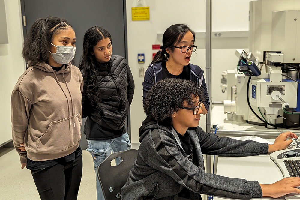
Held in November, EMERGE invited 18 eighth-grade students to the pilot event at MIT.nano, an interdisciplinary facility for nanoscale research, to get hands-on experience in microscopy and materials science.

The highlight of the two-hour workshop: Each student explored mystery samples of everyday materials using one of two scanning electron microscopes (SEMs), which scan material samples using a beam of electrons to form an image. Though highly sophisticated, the instruments generated readily understandable data — images of intricate structures in a butterfly wing or a strand of hair, for example.

The students had an immediate, tangible sense of success, says Thrasher, from MIT’s Department of Materials Science and Engineering (DMSE). He led the program along with Cai, also from DMSE, and Collette Gordon, a grad student in the Department of Chemistry.

“This experience helped build a sense of agency and autonomy around this area of science, nurturing budding self-confidence among the students,” Thrasher says. “We didn’t give the students instructions, just empowered them to solve problems. When you don’t tell them the solution, you get really surprised with what they come up with.”

Unlocking interest in the infinitesimal

The students were part of a multi-year science and engineering exploration program called MITES Saturdays, run by MIT Introduction to Technology, Engineering, and Science, or MITES. A team of volunteers was on hand to help students follow the guidance set out by Thrasher, ensuring the careful handling of the SEMs — worth roughly $500,000 each.

MITES Saturdays program administrator Lynsey Ford was thrilled to observe the students’ autonomous exploration and enthusiasm.

“Our students got to meet real scientists who listened to them, cared about the questions they were asking, and welcomed them into a world of science,” Ford says. “A supportive learning environment can be just as powerful for science discovery as a half-million-dollar microscope.”

The pilot workshop was the first step for Thrasher and his team in their goal to build EMERGE into a program with broad impact, engaging middle-to-high school students from a variety of communities.

The partnership with MITES Saturdays is crucial for this endeavor, says Thrasher, providing a platform to reach a wider audience. “Seeing students from diverse backgrounds participating in EMERGE reinforces the profound difference science education can have.”

MITES Saturdays students are high-achieving Massachusetts seventh through 12th graders from Boston, MIT’s hometown of Cambridge, and nearby Lawrence.

“The majority of students who participate in our programs would be the first person in their family to go to college. A lot of them are from families balancing some sort of financial hardship, and from populations that are historically underrepresented in STEM,” Ford says.

Experienced SEM users set up the instruments and prepared test samples so students could take turns exploring specimens such as burrs, butterfly wings, computer chips, hair, and pollen by operating the microscope to adjust magnification, focus, and stage location.

Students left the EMERGE event with copies of the electron microscope images they generated. Thrasher hopes they will use these materials in follow-up projects, ideally integrating them into existing school curricula so students can share their experiences.

EMERGE co-director Cai says students were excited with their experimentation, both in being able to access such high-end equipment and in seeing what materials like Velcro look like under an SEM (spoiler alert: it’s spaghetti).

“We definitely saw a spark,” Cai says. “The subject matter was complex, but the students always wanted to know more.” And the after-program feedback was positive, with most saying the experience was fun and challenging. The volunteers noted how engaged the students were with the SEMs and subject matter. One volunteer overheard students say, “I felt like a real scientist!”

Inspiring tomorrow’s scientists

EMERGE is based on the Scanning Electron Microscopy Educators program, a long-running STEM outreach program started in 1991 by the Air Force Research Laboratory and adopted by Michigan State University. As an Air Force captain stationed at Wright-Patterson Air Force Base in Ohio, Thrasher participated in the program as a volunteer SEM expert.

“I thought it was an incredible opportunity for young students and wanted to bring it here to MIT,” he says.

The pilot was made possible thanks to support from the MITES Saturdays team and the Graduate Materials Council (GMC), the DMSE graduate student organization. Cai and DMSE grad student Jessica Dong, who are both GMC outreach chairs, helped fund, organize, and coordinate the event.

The MITES Saturdays students included reflections on their experience with the SEMs in their final presentations at the MITES Fall Symposium in November.

“My favorite part of the semester was using the SEM as it introduced me to microscopy at the level of electrons,” said one student.

“Our students had an incredible time with the EMERGE team. We’re excited about the possibility of future partnerships with MIT.nano and other departments at MIT, giving our scholars exposure to the breadth of opportunities as future scientists,” says Eboney Hearn, MITES executive director.

With the success of the pilot, the EMERGE team is looking to offer more programs to the MITES students in the spring. Anna Osherov is excited to give students more access to the cumulative staff knowledge and cutting-edge equipment at MIT.nano, which opened in 2018. Osherov is associate director for Characterization.nano, a shared experimental facility for advanced imaging and analysis.

“Our mission is to support mature researchers — and to help inspire the future PhDs and professors who will come to MIT to learn, research, and innovate,” Osherov says. “Designing and offering such programs, aimed at fostering natural curiosity and creativity of young minds, has a tremendous long-term benefit to our society. We can raise tomorrow’s generation in a better way.”

For her part, Ford is still coasting on the students’ excitement. “They come into the program so curious and hungry for knowledge. They remind me every day how amazing the world is.”

© Photo courtesy of the EMERGE program.

Middle schoolers in the MITES Saturdays science program at MIT examine images of material samples through a scanning electron microscope at MIT.nano, with the help of Rebecca Li (third from left), a postdoc in the Department of Materials Science and Engineering. The students participated in a pilot education program called EMERGE aimed at engaging students in hands-on scientific exploration.

Capsid of HIV-1 behaves like cell’s cargo receptor to enter the nucleus

Retroviruses cannot replicate on their own — they must insert their genetic code into the DNA of a host and exploit the host cell's resources to make more copies of themselves, furthering infection. Some retroviruses only infect cells as they divide, when the nuclear envelope that protects the host's genetic material breaks down, making it easily accessible. HIV-1 is a type of retrovirus, called a lentivirus, that can infect non-dividing cells.

HIV-1 delivers its genome into the nucleus by packaging it into a large, cone-shaped structure called a capsid — but the exact mechanism has remained elusive for decades. Travel through the nuclear envelope occurs through, and is regulated by, nuclear pores, doughnut-shaped protein assemblies. Human cells have about 2,000 nuclear pores perforating the nuclear envelope. Some earlier evidence suggested that the capsid remains intact during its delivery into the nucleus — but this created a dimensional conundrum. The cone-shaped HIV-1 capsid is about 120 nanometers long and 60 nm wide — too large, researchers thought, to fit through the opening of the nuclear pore, measured at only 43 nm wide.

Members of the Schwartz Lab at MIT, in the Department of Biology, became interested in this question when a postdoc in the lab used cryo-electron tomography, slicing up sections of frozen cells to examine structures, to show that nuclear pores in the nuclear envelope are larger than 43nm. They deflate and shrink, it turns out, when removed from their native conditions. In native conditions, the nuclear pore complex is about 60nm wide — wide enough to accommodate the HIV-1 capsid.

Knowing that it could fit, a question remained: How can the capsid navigate the dense mesh of spaghetti-like proteins that act like a sieve in the nuclear pore channel? That spaghetti-like mesh allows small cargo to diffuse through, but prevents large cargo from entering unless it is escorted by proteins called nuclear transport receptors.

In an open-access paper published today in Nature, researchers present evidence that the HIV-1 capsid mimics the cell's transport receptors to traverse the nuclear pore.

To support that conclusion, the researchers showed three things in vitro: that an HIV-1 capsid can deliver cargo through a nuclear pore analog; that the capsid can interact with the sieve of proteins in the nuclear pore channel; and that the capsid targets the nuclear pore in the absence of native transport proteins.

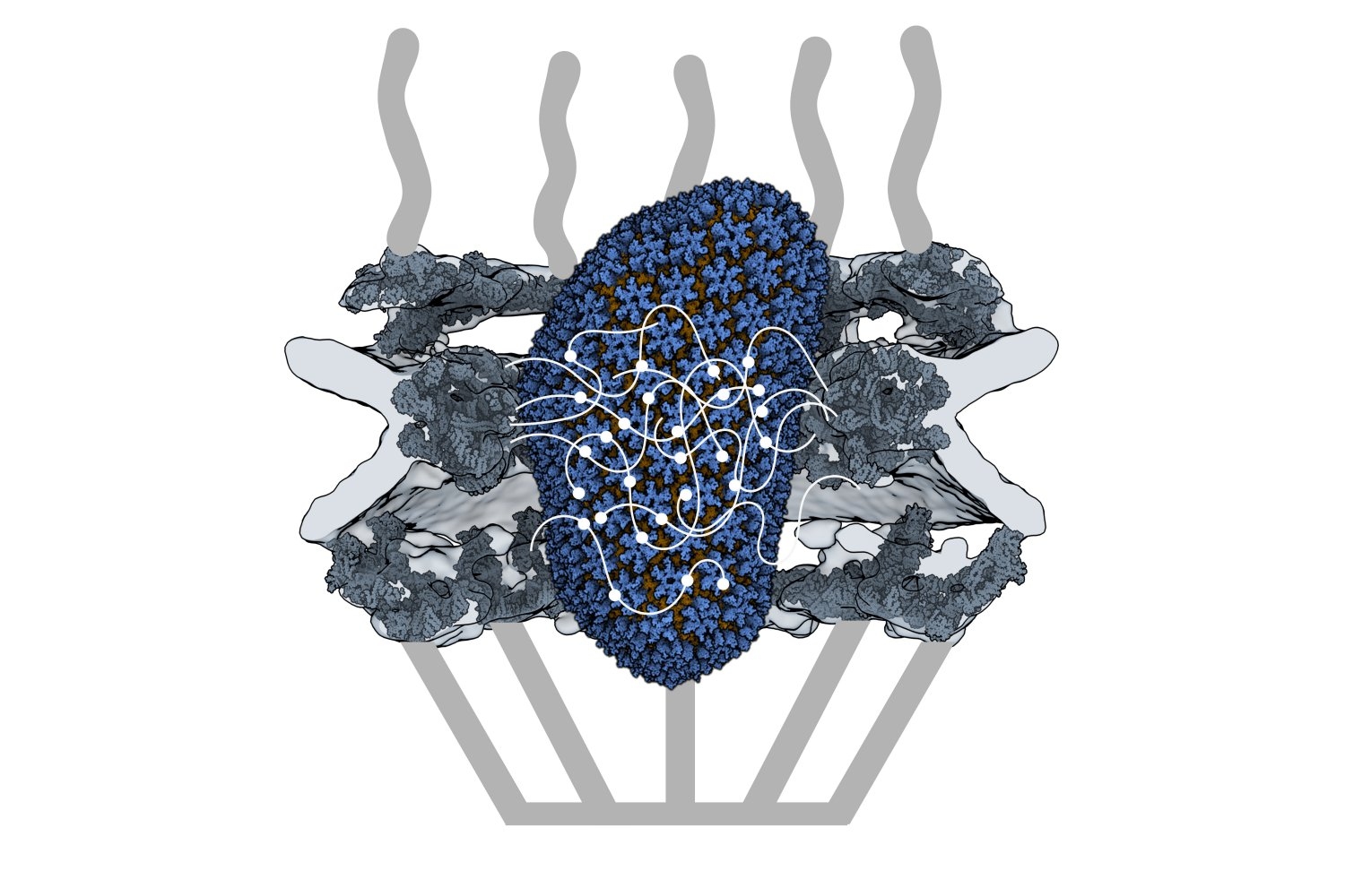
Nuclear transport receptors escort large cargo through the nuclear pore by “batting away” the spaghetti-like mesh of proteins inside the channel — like someone holding your hand and guiding you across a crowded dance floor. The HIV-1 capsid interacts with the spaghetti-like proteins, but its purpose is more like a Trojan horse — the capsid encapsulates the viral cargo, protecting it from detection in the cytoplasm and as it enters the nuclear pore complex.

"What's really amazing about cells is that they are incredibly complex. What's really difficult about studying cells is that they are incredibly complex," jokes co-first author Erika Weiskopf, a graduate student in the Schwartz lab. "Biochemists are constantly trying to find ways to study their system in a simplified context, but still give it a flavor of cell biology."

To do that, the Schwartz lab collaborated with Dirk Görlich, the director of cellular logistics at the Max Planck Institute for Multidisciplinary Sciences. Görlich is a co-senior author on the paper with MIT’s Boris Magasanik Professor of Biology Thomas Schwartz. Görlich's lab has produced concentrated droplets of the spaghetti-like proteins found inside the nuclear pore, and those droplets allow and exclude cargo the same way a nuclear pore will. In experiments, fluorescently-labeled cargo did not enter the droplets, but fluorescently-labeled cargo packaged in an HIV-1 capsid was delivered. This indicated that the capsid could deliver cargo through a nuclear pore. 

Using a biophysical binding assay, the researchers also showed that the HIV-1 capsid interacts with the proteins inside the channel. Different spaghetti-like proteins are found in different channel sections, such as at the cytoplasmic side's entrance or only inside the channel; there are 10 such proteins in human cells. The capsid is a promiscuous binder — it can interact with all the spaghetti-like proteins found in the channel.

The capsid can target the nuclear pore complex even without the cell's transport receptors, indicating that it is not commandeering native transport receptors to find and enter the nuclear pore. The team used a classic assay in the nucleocytoplasmic transport field to collect this evidence: When cells are treated with digitonin, their membranes become porous. Everything in the cytoplasm will leak out of the cells, but the nuclear envelope will remain intact. Despite the absence of native proteins, the capsid was attracted to the nuclear pore complex, a behavior indicative of a nuclear transport receptor.

Although the capsid behaves like a nuclear transport receptor to penetrate the nuclear pore, it is fundamentally different. A transport receptor doesn't need to conceal material for delivery the way the capsid does to avoid detection.

These findings open new lines of inquiry for what the nuclear pore complex is capable of accommodating.

"The HIV-1 capsid is one of the largest things that we now know can go through the nuclear pore complex intact," Weiskopf says. "It raises all kinds of questions — what other things could be going through the pore that we thought was impossible?"

Schwartz said another question is whether all of the 2,000 nuclear pores in human cells are identical or whether there is something that makes certain pores more amenable to allowing the capsid through.

The capsid is also known to be unusually elastic, a property that may be key for passage through the pore. Another interesting question for the field is whether the cone-shaped capsid gains entry into the pore by squeezing through.

Although the team has shown that the capsid can enter the pore, what happens at the other end of the channel is still unknown — whether the capsid fully or partially enters the nucleus or breaks down inside the channel. Weiskopf is working on perturbing parts of the capsid or the spaghetti-like proteins to learn more about which interactions are most important for successful capsid entry.

Although these results have expanded our understanding of the nuclear pore, much remains unknown, both for HIV-1 infection and for the transport process through the nuclear pore complex.  

"The nuclear pore is such an important element of cell biology, we thought it would be interesting to understand it better — and that's how we figured out that the pore is much bigger than we anticipated," Schwartz says. "We will certainly try to see whether we can understand the mechanism of HIV-1 infection, how the capsid is released on the other side of the channel, and what factors are important there — and to what extent you can manipulate it or influence it for therapeutic applications."

This research was carried out, in part, using MIT.nano facilities.

© Image courtesy of the Schwartz Lab.

An HIV-1 capsid penetrates a nuclear pore complex by interacting with the spaghetti-like proteins inside the channel, behaving like the cell’s own cargo transport proteins.
  • ✇MIT News - Nanoscience and nanotechnology | MIT.nano
  • Celebrating five years of MIT.nanoAmanda Stoll DiCristofaro | MIT.nano
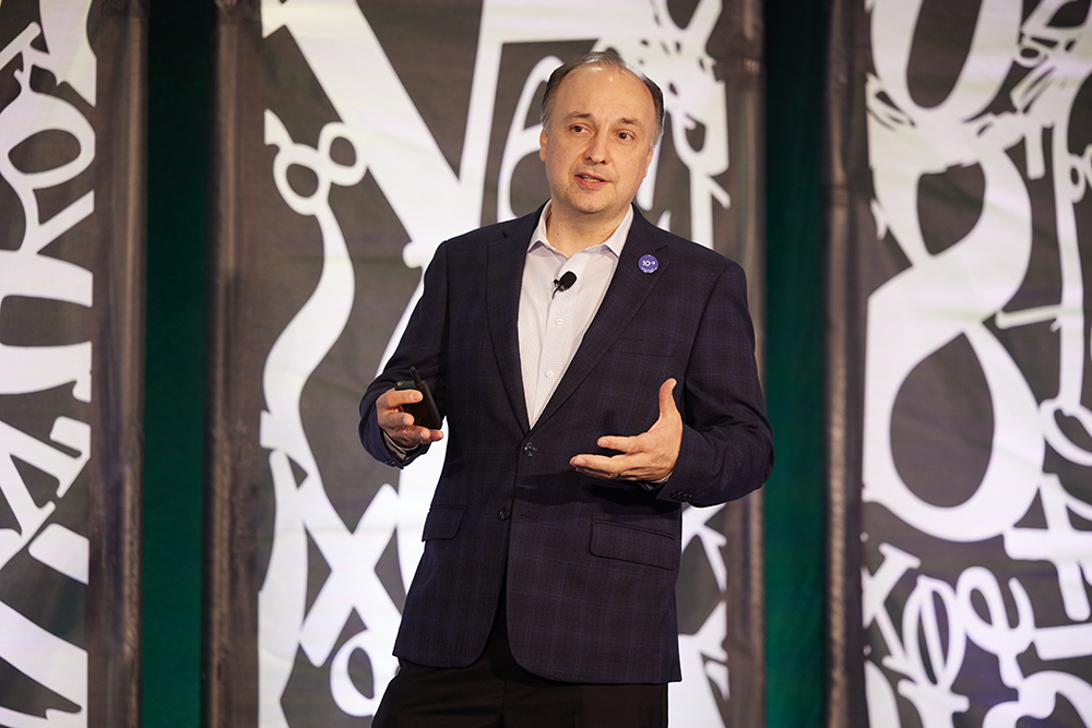
    There is vast opportunity for nanoscale innovation to transform the world in positive ways — expressed MIT.nano Director Vladimir Bulović as he posed two questions to attendees at the start of the inaugural Nano Summit: “Where are we heading? And what is the next big thing we can develop?” “The answer to that puts into perspective our main purpose — and that is to change the world,” Bulović, the Fariborz Maseeh Professor of Emerging Technologies, told an audience of more than 325 in-person and
     

Celebrating five years of MIT.nano

There is vast opportunity for nanoscale innovation to transform the world in positive ways — expressed MIT.nano Director Vladimir Bulović as he posed two questions to attendees at the start of the inaugural Nano Summit: “Where are we heading? And what is the next big thing we can develop?”

“The answer to that puts into perspective our main purpose — and that is to change the world,” Bulović, the Fariborz Maseeh Professor of Emerging Technologies, told an audience of more than 325 in-person and 150 virtual participants gathered for an exploration of nano-related research at MIT and a celebration of MIT.nano’s fifth anniversary.

Over a decade ago, MIT embarked on a massive project for the ultra-small — building an advanced facility to support research at the nanoscale. Construction of MIT.nano in the heart of MIT’s campus, a process compared to assembling a ship in a bottle, began in 2015, and the facility launched in October 2018.

Fast forward five years: MIT.nano now contains nearly 170 tools and instruments serving more than 1,200 trained researchers. These individuals come from over 300 principal investigator labs, representing more than 50 MIT departments, labs, and centers. The facility also serves external users from industry, other academic institutions, and over 130 startup and multinational companies. And in 2022, MIT.nano's home — Building 12 — was named in honor of Lisa T. Su ’90, SM ’91, PhD ’94, chief executive officer and chair of the Board of Directors of AMD.

A cross section of these faculty and researchers joined industry partners and MIT community members to kick off the first Nano Summit, which is expected to become an annual flagship event for MIT.nano and its industry consortium. Held on Oct. 24, the inaugural conference was co-hosted by the MIT Industrial Liaison Program.

Six topical sessions highlighted recent developments in quantum science and engineering, materials, advanced electronics, energy, biology, and immersive data technology. The Nano Summit also featured startup ventures and an art exhibition.

Watch the videos here.

Seeing and manipulating at the nanoscale — and beyond

“We need to develop new ways of building the next generation of materials,” said Frances Ross, the TDK Professor in Materials Science and Engineering (DMSE). “We need to use electron microscopy to help us understand not only what the structure is after it’s built, but how it came to be. I think the next few years in this piece of the nano realm are going to be really amazing.”

Speakers in the session “The Next Materials Revolution,” chaired by MIT.nano co-director for Characterization.nano and associate professor in DMSE James LeBeau, highlighted areas in which cutting-edge microscopy provides insights into the behavior of functional materials at the nanoscale, from anti-ferroelectrics to thin-film photovoltaics and 2D materials. They shared images and videos collected using the instruments in MIT.nano’s characterization suites, which were specifically designed and constructed to minimize mechanical-vibrational and electro-magnetic interference.

Later, in the “Biology and Human Health” session chaired by Boris Magasanik Professor of Biology Thomas Schwartz, biologists echoed the materials scientists, stressing the importance of the ultra-quiet, low-vibration environment in Characterization.nano to obtain high-resolution images of biological structures.

“Why is MIT.nano important for us?” asked Schwartz. “An important element of biology is to understand the structure of biology macromolecules. We want to get to an atomic resolution of these structures. CryoEM (cryo-electron microscopy) is an excellent method for this. In order to enable the resolution revolution, we had to get these instruments to MIT. For that, MIT.nano was fantastic.”

Seychelle Vos, the Robert A. Swanson (1969) Career Development Professor of Life Sciences, shared CryoEM images from her lab’s work, followed by biology Associate Professor Joey Davis who spoke about image processing. When asked about the next stage for CryoEM, Davis said he’s most excited about in-situ tomography, noting that there are new instruments being designed that will improve the current labor-intensive process.

To chart the future of energy, chemistry associate professor Yogi Surendranath is also using MIT.nano to see what is happening at the nanoscale in his research to use renewable electricity to change carbon dioxide into fuel.

“MIT.nano has played an immense role, not only in facilitating our ability to make nanostructures, but also to understand nanostructures through advanced imaging capabilities,” said Surendranath. “I see a lot of the future of MIT.nano around the question of how nanostructures evolve and change under the conditions that are relevant to their function. The tools at MIT.nano can help us sort that out.”

Tech transfer and quantum computing

The “Advanced Electronics” session chaired by Jesús del Alamo, the Donner Professor of Science in the Department of Electrical Engineering and Computer Science (EECS), brought together industry partners and MIT faculty for a panel discussion on the future of semiconductors and microelectronics. “Excellence in innovation is not enough, we also need to be excellent in transferring these to the marketplace,” said del Alamo. On this point, panelists spoke about strengthening the industry-university connection, as well as the importance of collaborative research environments and of access to advanced facilities, such as MIT.nano, for these environments to thrive.

The session came on the heels of a startup exhibit in which eleven START.nano companies presented their technologies in health, energy, climate, and virtual reality, among other topics. START.nano, MIT.nano’s hard-tech accelerator, provides participants use of MIT.nano’s facilities at a discounted rate and access to MIT’s startup ecosystem. The program aims to ease hard-tech startups’ transition from the lab to the marketplace, surviving common “valleys of death” as they move from idea to prototype to scaling up.

When asked about the state of quantum computing in the “Quantum Science and Engineering” session, physics professor Aram Harrow related his response to these startup challenges. “There are quite a few valleys to cross — there are the technical valleys, and then also the commercial valleys.” He spoke about scaling superconducting qubits and qubits made of suspended trapped ions, and the need for more scalable architectures, which we have the ingredients for, he said, but putting everything together is quite challenging.

Throughout the session, William Oliver, professor of physics and the Henry Ellis Warren (1894) Professor of Electrical Engineering and Computer Science, asked the panelists how MIT.nano can address challenges in assembly and scalability in quantum science.

“To harness the power of students to innovate, you really need to allow them to get their hands dirty, try new things, try all their crazy ideas, before this goes into a foundry-level process,” responded Kevin O’Brien, associate professor in EECS. “That’s what my group has been working on at MIT.nano, building these superconducting quantum processors using the state-of-the art fabrication techniques in MIT.nano.”

Connecting the digital to the physical

In his reflections on the semiconductor industry, Douglas Carlson, senior vice president for technology at MACOM, stressed connecting the digital world to real-world application. Later, in the “Immersive Data Technology” session, MIT.nano associate director Brian Anthony explained how, at the MIT.nano Immersion Lab, researchers are doing just that.

“We think about and facilitate work that has the human immersed between hardware, data, and experience,” said Anthony, principal research scientist in mechanical engineering. He spoke about using the capabilities of the Immersion Lab to apply immersive technologies to different areas — health, sports, performance, manufacturing, and education, among others. Speakers in this session gave specific examples in hardware, pediatric health, and opera.

Anthony connected this third pillar of MIT.nano to the fab and characterization facilities, highlighting how the Immersion Lab supports work conducted in other parts of the building. The Immersion Lab’s strength, he said, is taking novel work being developed inside MIT.nano and bringing it up to the human scale to think about applications and uses.

Artworks that are scientifically inspired

The Nano Summit closed with a reception at MIT.nano where guests could explore the facility and gaze through the cleanroom windows, where users were actively conducting research. Attendees were encouraged to visit an exhibition on MIT.nano’s first- and second-floor galleries featuring work by students from the MIT Program in Art, Culture, and Technology (ACT) who were invited to utilize MIT.nano’s tool sets and environments as inspiration for art.

In his closing remarks, Bulović reflected on the community of people who keep MIT.nano running and who are using the tools to advance their research. “Today we are celebrating the facility and all the work that has been done over the last five years to bring it to where it is today. It is there to function not just as a space, but as an essential part of MIT’s mission in research, innovation, and education. I hope that all of us here today take away a deep appreciation and admiration for those who are leading the journey into the nano age.”

© Photo: Jared Charney

MIT faculty and researchers participate in a panel discussion on quantum science and engineering. Left to right: Professor Aram Harrow, Professor Paola Cappellaro, Associate Professor Kevin O'Brien, Research Scientist Jeff Grover, and session chair Professor William Oliver.
  • ✇MIT News - Nanoscience and nanotechnology | MIT.nano
  • Using AI to optimize for rapid neural imagingRachel Gordon | MIT CSAIL
    Connectomics, the ambitious field of study that seeks to map the intricate network of animal brains, is undergoing a growth spurt. Within the span of a decade, it has journeyed from its nascent stages to a discipline that is poised to (hopefully) unlock the enigmas of cognition and the physical underpinning of neuropathologies such as in Alzheimer’s disease.  At its forefront is the use of powerful electron microscopes, which researchers from the MIT Computer Science and Artificial Intelligence
     

Using AI to optimize for rapid neural imaging

Connectomics, the ambitious field of study that seeks to map the intricate network of animal brains, is undergoing a growth spurt. Within the span of a decade, it has journeyed from its nascent stages to a discipline that is poised to (hopefully) unlock the enigmas of cognition and the physical underpinning of neuropathologies such as in Alzheimer’s disease. 

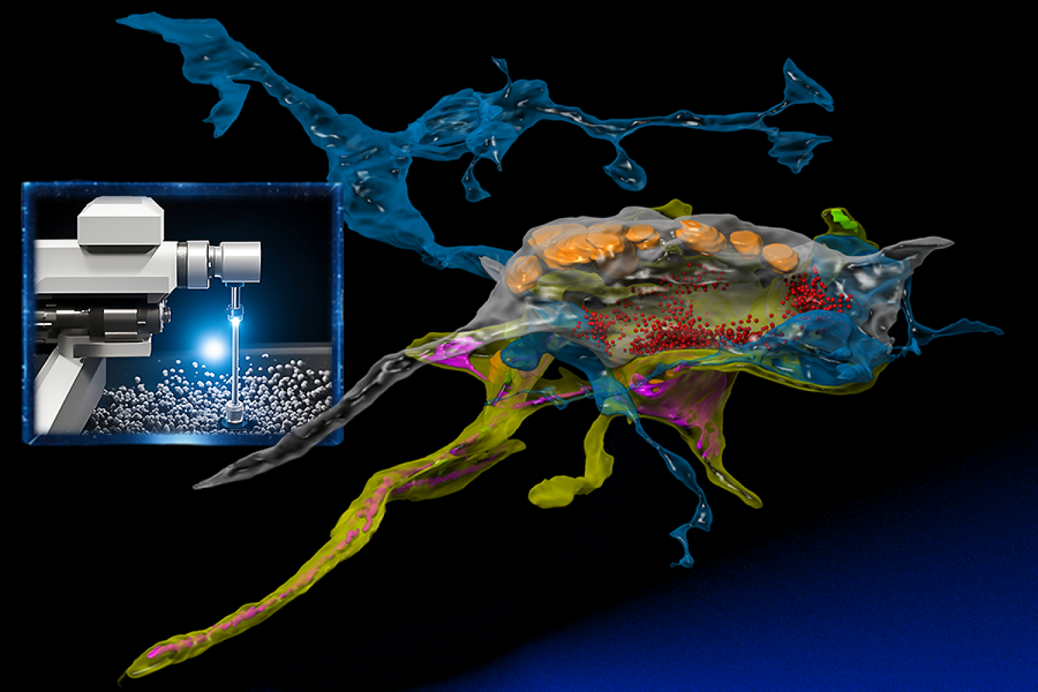
At its forefront is the use of powerful electron microscopes, which researchers from the MIT Computer Science and Artificial Intelligence Laboratory (CSAIL) and the Samuel and Lichtman Labs of Harvard University bestowed with the analytical prowess of machine learning. Unlike traditional electron microscopy, the integrated AI serves as a “brain” that learns a specimen while acquiring the images, and intelligently focuses on the relevant pixels at nanoscale resolution similar to how animals inspect their worlds. 

SmartEM” assists connectomics in quickly examining and reconstructing the brain’s complex network of synapses and neurons with nanometer precision. Unlike traditional electron microscopy, its integrated AI opens new doors to understand the brain's intricate architecture.

The integration of hardware and software in the process is crucial. The team embedded a GPU into the support computer connected to their microscope. This enabled running machine-learning models on the images, helping the microscope beam be directed to areas deemed interesting by the AI. “This lets the microscope dwell longer in areas that are harder to understand until it captures what it needs,” says MIT professor and CSAIL principal investigator Nir Shavit. “This step helps in mirroring human eye control, enabling rapid understanding of the images.” 

“When we look at a human face, our eyes swiftly navigate to the focal points that deliver vital cues for effective communication and comprehension,” says the lead architect of SmartEM, Yaron Meirovitch, a visiting scientist at MIT CSAIL who is also a former postdoc and current research associate neuroscientist at Harvard. “When we immerse ourselves in a book, we don't scan all of the empty space; rather, we direct our gaze towards the words and characters with ambiguity relative to our sentence expectations. This phenomenon within the human visual system has paved the way for the birth of the novel microscope concept.” 

For the task of reconstructing a human brain segment of about 100,000 neurons, achieving this with a conventional microscope would necessitate a decade of continuous imaging and a prohibitive budget. However, with SmartEM, by investing in four of these innovative microscopes at less than $1 million each, the task could be completed in a mere three months.

Nobel Prizes and little worms  

Over a century ago, Spanish neuroscientist Santiago Ramón y Cajal was heralded as being the first to characterize the structure of the nervous system. Employing the rudimentary light microscopes of his time, he embarked on leading explorations into neuroscience, laying the foundational understanding of neurons and sketching the initial outlines of this expansive and uncharted realm — a feat that earned him a Nobel Prize. He noted, on the topics of inspiration and discovery, that “As long as our brain is a mystery, the universe, the reflection of the structure of the brain will also be a mystery.”

Progressing from these early stages, the field has advanced dramatically, evidenced by efforts in the 1980s, mapping the relatively simpler connectome of C. elegans, small worms, to today’s endeavors probing into more intricate brains of organisms like zebrafish and mice. This evolution reflects not only enormous strides, but also escalating complexities and demands: mapping the mouse brain alone means managing a staggering thousand petabytes of data, a task that vastly eclipses the storage capabilities of any university, the team says. 

Testing the waters

For their own work, Meirovitch and others from the research team studied 30-nanometer thick slices of octopus tissue that were mounted on tapes, put on wafers, and finally inserted into the electron microscopes. Each section of an octopus brain, comprising billions of pixels, was imaged, letting the scientists reconstruct the slices into a three-dimensional cube at nanometer resolution. This provided an ultra-detailed view of synapses. The chief aim? To colorize these images, identify each neuron, and understand their interrelationships, thereby creating a detailed map or “connectome” of the brain's circuitry.

“SmartEM will cut the imaging time of such projects from two weeks to 1.5 days,” says Meirovitch. “Neuroscience labs that currently can't be engaged with expensive and long EM imaging will be able to do it now,” The method should also allow synapse-level circuit analysis in samples from patients with psychiatric and neurologic disorders. 

Down the line, the team envisions a future where connectomics is both affordable and accessible. They hope that with tools like SmartEM, a wider spectrum of research institutions could contribute to neuroscience without relying on large partnerships, and that the method will soon be a standard pipeline in cases where biopsies from living patients are available. Additionally, they’re eager to apply the tech to understand pathologies, extending utility beyond just connectomics. “We are now endeavoring to introduce this to hospitals for large biopsies, utilizing electron microscopes, aiming to make pathology studies more efficient,” says Shavit. 

Two other authors on the paper have MIT CSAIL ties: lead author Lu Mi MCS ’19, PhD ’22, who is now a postdoc at the Allen Institute for Brain Science, and Shashata Sawmya, an MIT graduate student in the lab. The other lead authors are Core Francisco Park and Pavel Potocek, while Harvard professors Jeff Lichtman and Aravi Samuel are additional senior authors. Their research was supported by the NIH BRAIN Initiative and was presented at the 2023 International Conference on Machine Learning (ICML) Workshop on Computational Biology. The work was done in collaboration with scientists from Thermo Fisher Scientific.

© Left image: Yaron Meirovitch via the Stable Diffusion XL AI image generator and Alex Shipps via the Midjourney AI image generator. Right image: Daniel Berger and Meirovitch, edited by Alex Shipps/MIT CSAIL

MIT researchers invented a technology and software to take electron microscopy to the next level by seamlessly integrating real-time machine learning into the imaging process — “smart microscopy.”
❌
❌