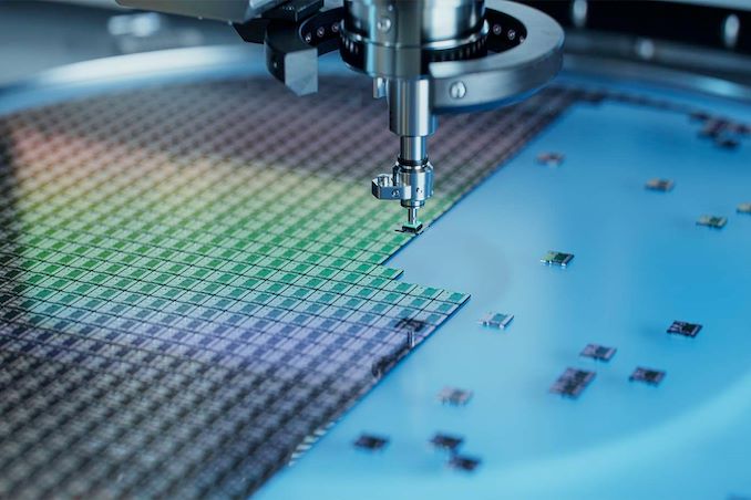
One of the core challenges that Rapidus will face when it kicks off volume production of chips on its 2nm-class process technology in 2027 is lining up customers. With Intel, Samsung, and TSMC all slated to offer their own 2nm-class nodes by that time, Rapidus will need some kind of advantage to attract customers away from its more established rivals. To that end, the company thinks they've found their edge: fully automated packaging that will allow for shorter chip lead times than manned packag
One of the core challenges that Rapidus will face when it kicks off volume production of chips on its 2nm-class process technology in 2027 is lining up customers. With Intel, Samsung, and TSMC all slated to offer their own 2nm-class nodes by that time, Rapidus will need some kind of advantage to attract customers away from its more established rivals. To that end, the company thinks they've found their edge: fully automated packaging that will allow for shorter chip lead times than manned packaging operations.
In an interview with Nikkei, Rapidus' president, Atsuyoshi Koike, outlined the company's vision to use advanced packaging as a competitive edge for the new fab. The Hokkaido facility, which is currently under construction and is expecting to begin equipment installation this December, is already slated to both produce chips and offer advanced packaging services within the same facility, an industry first. But ultimately, Rapidus biggest plan to differentiate itself is by automating the back-end fab processes (chip packaging) to provide significantly faster turnaround times.
Rapidus is targetting back-end production in particular as, compared to front-end (lithography) production, back-end production still heavily relies on human labor. No other advanced packaging fab has fully automated the process thus far, which provides for a degree of flexibility, but slows throughput. But with automation in place to handle this aspect of chip production, Rapidus would be able to increase chip packaging efficiency and speed, which is crucial as chip assembly tasks become more complex. Rapidus is also collaborating with multiple Japanese suppliers to source materials for back-end production.
"In the past, Japanese chipmakers tried to keep their technology development exclusively in-house, which pushed up development costs and made them less competitive," Koike told Nikkei. "[Rapidus plans to] open up technology that should be standardized, bringing down costs, while handling important technology in-house."
Financially, Rapidus faces a significant challenge, needing a total of ¥5 trillion ($35 billion) by the time mass production starts in 2027. The company estimates that ¥2 trillion will be required by 2025 for prototype production. While the Japanese government has provided ¥920 billion in aid, Rapidus still needs to secure substantial funding from private investors.
Due to its lack of track record and experience of chip production as. well as limited visibility for success, Rapidus is finding it difficult to attract private financing. The company is in discussions with the government to make it easier to raise capital, including potential loan guarantees, and is hopeful that new legislation will assist in this effort.
Under the CHIPS & Science Act, the U.S. government provided tens of billions of dollars in grants and loans to the world's leading maker of chips, such as Intel, Samsung, and TSMC, which will significantly expand the country's semiconductor production industry in the coming years. However, most chips are typically tested, assembled, and packaged in Asia, which has left the American supply chain incomplete. Addressing this last gap in the government's domestic chip production plans, these pas
Under the CHIPS & Science Act, the U.S. government provided tens of billions of dollars in grants and loans to the world's leading maker of chips, such as Intel, Samsung, and TSMC, which will significantly expand the country's semiconductor production industry in the coming years. However, most chips are typically tested, assembled, and packaged in Asia, which has left the American supply chain incomplete. Addressing this last gap in the government's domestic chip production plans, these past couple of weeks the U.S. government signed memorandums of understanding worth about $1.5 billion with Amkor and SK hynix to support their efforts to build chip packaging facilities in the U.S.
Amkor to Build Advanced Packaging Facility with Apple in Mind
Amkor plans to build a $2 billion advanced packaging facility near Peoria, Arizona, to test and assemble chips produced by TSMC at its Fab 21 near Phoenix, Arizona. The company signed a MOU that offers $400 million in direct funding and access to $200 million in loans under the CHIPS & Science Act. In addition, the company plans to take advantage of a 25% investment tax credit on eligible capital expenditures.
Set to be strategically positioned near TSMC's upcoming Fab 21 complex in Arizona, Amkor's Peoria facility will occupy 55 acres and, when fully completed, will feature over 500,000 square feet (46,451 square meters) of cleanroom space, more than twice the size of Amkor's advanced packaging site in Vietnam. Although the company has not disclosed the exact capacity or the specific technologies the facility will support, it is expected to cater to a wide range of industries, including automotive, high-performance computing, and mobile technologies. This suggests the new plant will offer diverse packaging solutions, including traditional, 2.5D, and 3D technologies.
Amkor has collaborated extensively with Apple on the vision and initial setup of the Peoria facility, as Apple is slated to be the facility's first and largest customer, marking a significant commitment from the tech giant. This partnership highlights the importance of the new facility in reinforcing the U.S. semiconductor supply chain and positioning Amkor as a key partner for companies relying on TSMC's manufacturing capabilities. The project is expected to generate around 2,000 jobs and is scheduled to begin operations in 2027.
SK hynix to Build HBM4 in the U.S.
This week SK hynix also signed a preliminary agreement with the U.S. government to receive up to $450 million in direct funding and $500 million in loans to build an advanced memory packaging facility in West Lafayette, Indiana.
The proposed facility is scheduled to begin operations in 2028, which means that it will assemble HBM4 or HBM4E memory. Meanwhile, DRAM devices for high bandwidth memory (HBM) stacks will still be produced in South Korea. Nonetheless, packing finished HBM4/HBM4E in the U.S. and possibly integrating these memory modules with high-end processors is a big deal.
In addition to building its packaging plant, SK hynix plans to collaborate with Purdue University and other local research institutions to advance semiconductor technology and packaging innovations. This partnership is intended to bolster research and development in the region, positioning the facility as a hub for AI technology and skilled employment.
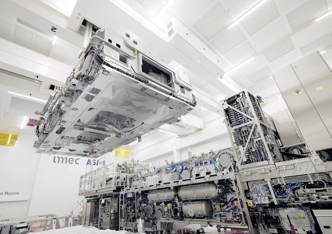
Imec and ASML have announced that the two companies have printed the first logic and DRAM patterns using ASML's experimental Twinscan EXE:5000 EUV lithography tool, the industry's first High-NA EUV scanner. The lithography system achieved resolution that is good enough for 1.4nm-class process technology with just one exposure, which confirms the capabilities of the system and that development of the High-NA ecosystem remains on-track for use in commercial chip production later this decade.
"The
Imec and ASML have announced that the two companies have printed the first logic and DRAM patterns using ASML's experimental Twinscan EXE:5000 EUV lithography tool, the industry's first High-NA EUV scanner. The lithography system achieved resolution that is good enough for 1.4nm-class process technology with just one exposure, which confirms the capabilities of the system and that development of the High-NA ecosystem remains on-track for use in commercial chip production later this decade.
"The results confirm the long-predicted resolution capability of High NA EUV lithography, targeting sub 20nm pitch metal layers in one single exposure," said Luc Van den hove, president and CEO of imec. "High NA EUV will therefore be highly instrumental to continue the dimensional scaling of logic and memory technologies, one of the key pillars to push the roadmaps deep into the ‘angstrom era'. These early demonstrations were only possible thanks to the set-up of the joint ASML-imec lab allowing our partners to accelerate the introduction of High NA lithography into manufacturing."
The successful test printing comes after ASML and Imec have spent the last several months laying the groundwork for the test. Besides the years required to build the complex scanner itself, engineers from ASML, Imec, and their partners needed to develop newer photoresists, underlayers, and reticles. Then they had to take an existing production node and tune it for High-NA EUV tools, including doing optical proximity correction (OPC) and tuning etching processes.
The culmination of these efforts was that, using ASML's pre-production Twinscan EXE:5000 system, Imec was able to successfully pattern random logic structures with 9.5nm dense metal lines, which corresponds to a 19nm pitch and sub-20nm tip-to-tip dimensions. Similarly, Imec also set new high marks in feature density in other respects, including patterning of 2D features at a 22nm pitch, and printing random vias with a 30nm center-to-center distance, demonstrating high pattern fidelity and critical dimension uniformity.
The overall result is that Imec's experiments have proven that ASML's High-NA scanner is delivering on its intended capabilities, printing features at a fine enough resolution for fabricating logic on a 1.4nm-class process technology – and all with a single exposure. The latter is perhaps the most important aspect of this tooling, as the high cost and complexity of the High-NA tool itself (said to be around $400 million) is intended to be offset by being able to return to single-patterning, which allows for higher tool productivity and fewer steps overall.
Imec hasn't just been printing logic structures, either; the group successfully patterned DRAM designs as well, printing both a storage node landing pad alongside the bit line periphery for memory in a single exposure. As with their logic tests, this would allow DRAM designs to be printed in just one exposure, reducing cycle times and eventually costs.
9,5nm random logic structure (19nm pitch) after pattern transfer
"We are thrilled to demonstrate the world's first High NA-enabled logic and memory patterning in the joint ASML-imec lab as an initial validation of industry applications," said Steven Scheer, senior vice president of compute technologies & systems/compute system scaling at imec. "The results showcase the unique potential for High NA EUV to enable single-print imaging of aggressively-scaled 2D features, improving design flexibility as well as reducing patterning cost and complexity. Looking ahead, we expect to provide valuable insights to our patterning ecosystem partners, supporting them in further maturing High NA EUV specific materials and equipment."
South Korea's early trade data showed exports gaining momentum this month, boosting the outlook for economic growth and suggesting global demand for semiconductors remains resilient.
South Korea's early trade data showed exports gaining momentum this month, boosting the outlook for economic growth and suggesting global demand for semiconductors remains resilient.
Chinese exports of critical minerals are returning to more normal levels, undercutting fears that the restrictions imposed by the government last year could choke off supplies crucial to high-tech manufacturers around the world.
Chinese exports of critical minerals are returning to more normal levels, undercutting fears that the restrictions imposed by the government last year could choke off supplies crucial to high-tech manufacturers around the world.
Since 2012, Taiwan's integrated circuit (IC) industry has experienced positive growth for 11 consecutive years. Since 2014, it has officially surpassed the petroleum, coal products, and chemical raw materials industries to become the leading sector in manufacturing.
Since 2012, Taiwan's integrated circuit (IC) industry has experienced positive growth for 11 consecutive years. Since 2014, it has officially surpassed the petroleum, coal products, and chemical raw materials industries to become the leading sector in manufacturing.
Following the UK general election, attention has shifted to the country's national semiconductor strategy. An upcoming report urges the new government to conduct a comprehensive review of the semiconductor supply chain to ensure effective resource allocation.
Following the UK general election, attention has shifted to the country's national semiconductor strategy. An upcoming report urges the new government to conduct a comprehensive review of the semiconductor supply chain to ensure effective resource allocation.
Having received a subsidy of EUR10 billion (US$11 billion) from the German government to complete construction and start production within three years, what is the newest progress on Intel's Magdeburg fab factory?
Having received a subsidy of EUR10 billion (US$11 billion) from the German government to complete construction and start production within three years, what is the newest progress on Intel's Magdeburg fab factory?
TSMC's first European wafer fab is set to be located in Dresden, Germany, a region already recognized as a significant chip manufacturing hub in both Germany and Europe. This decision is expected to bring greater international geopolitical attention to the area, placing it at the forefront of the ongoing US-China chip war.
TSMC's first European wafer fab is set to be located in Dresden, Germany, a region already recognized as a significant chip manufacturing hub in both Germany and Europe. This decision is expected to bring greater international geopolitical attention to the area, placing it at the forefront of the ongoing US-China chip war.
ZillTek Technology, a micro-electromechanical systems (MEMS) microphone specialist, anticipates that demand for automotive, hearing aid, and headset applications will fuel future revenue growth.
ZillTek Technology, a micro-electromechanical systems (MEMS) microphone specialist, anticipates that demand for automotive, hearing aid, and headset applications will fuel future revenue growth.
IC distributor WPG posted strong revenue figures for the second quarter of 2024, with vice president Scott Lin expecting the third quarter to be the peak of the year in terms of both market growth and prices, and an optimistic outlook for the latter half of 2024.
IC distributor WPG posted strong revenue figures for the second quarter of 2024, with vice president Scott Lin expecting the third quarter to be the peak of the year in terms of both market growth and prices, and an optimistic outlook for the latter half of 2024.
Taiwan Specialty Chemicals (TSC) has gradually expanded its share of the global disilane market, which is dominated by its Japan- and France-based counterparts.
Taiwan Specialty Chemicals (TSC) has gradually expanded its share of the global disilane market, which is dominated by its Japan- and France-based counterparts.
Printed circuit board (PCB) and IC substrate equipment specialist Group Up Industrial (GP) has stepped up the development of its glass substrate offering, eyeing robust demand for advanced packaging.
Printed circuit board (PCB) and IC substrate equipment specialist Group Up Industrial (GP) has stepped up the development of its glass substrate offering, eyeing robust demand for advanced packaging.
Support from local foundries and backend houses in China is helping CMOS image sensor (CIS) firms obtain more orders, reducing the country's reliance on Sony, according to industry sources.
Support from local foundries and backend houses in China is helping CMOS image sensor (CIS) firms obtain more orders, reducing the country's reliance on Sony, according to industry sources.
Microchip Technology experienced a cyberattack on August 17 that disrupted its operations. The company is investigating the incident and working to restore normal business functions. The impact on the company's financial condition remains uncertain.
Microchip Technology experienced a cyberattack on August 17 that disrupted its operations. The company is investigating the incident and working to restore normal business functions. The impact on the company's financial condition remains uncertain.
ESMC has commenced construction on a new semiconductor fabrication facility in Dresden, Germany. The joint venture between TSMC, Robert Bosch, Infineon, and NXP is investing over EUR10 billion (US$11 billion) to establish the EU's first FinFET-capable pure-play foundry. This facility is anticipated to enhance semiconductor manufacturing capabilities in Europe and generate significant employment opportunities.
ESMC has commenced construction on a new semiconductor fabrication facility in Dresden, Germany. The joint venture between TSMC, Robert Bosch, Infineon, and NXP is investing over EUR10 billion (US$11 billion) to establish the EU's first FinFET-capable pure-play foundry. This facility is anticipated to enhance semiconductor manufacturing capabilities in Europe and generate significant employment opportunities.
Many chipmakers have disclosed delays or suspensions in their new European fab projects; however, TSMC's are proceeding more efficiently than those of their competitors.
Many chipmakers have disclosed delays or suspensions in their new European fab projects; however, TSMC's are proceeding more efficiently than those of their competitors.
TSMC Chairman C. C. Wei welcomes German Chancellor Olaf Scholz at Dresden plant. Credit: DIGITIMES
European Semiconductor Manufacturing Company (ESMC), a joint venture between TSMC, Robert Bosch, Infineon Technologies and NXP Semiconductors, has held a groundbreaking ceremony to officially mark the initial phase of land preparation for its first semiconductor fab in Dresden, Germany. The event brought together government officials, customers, suppliers, business partners and academia to celebrate a milestone in establishing what will be the EU's first-ever FinFET-capable pure-play foundry.
European Semiconductor Manufacturing Company (ESMC), a joint venture between TSMC, Robert Bosch, Infineon Technologies and NXP Semiconductors, has held a groundbreaking ceremony to officially mark the initial phase of land preparation for its first semiconductor fab in Dresden, Germany. The event brought together government officials, customers, suppliers, business partners and academia to celebrate a milestone in establishing what will be the EU's first-ever FinFET-capable pure-play foundry.
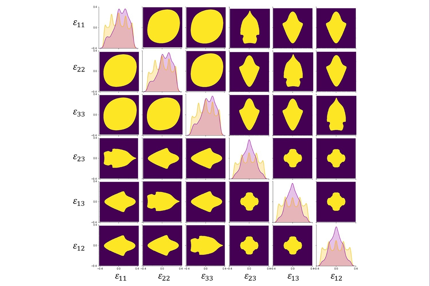
Without a map, it can be just about impossible to know not just where you are, but where you’re going, and that’s especially true when it comes to materials properties.
For decades, scientists have understood that while bulk materials behave in certain ways, those rules can break down for materials at the micro- and nano-scales, and often in surprising ways. One of those surprises was the finding that, for some materials, applying even modest strains — a concept known as elastic strain engineer
Without a map, it can be just about impossible to know not just where you are, but where you’re going, and that’s especially true when it comes to materials properties.
For decades, scientists have understood that while bulk materials behave in certain ways, those rules can break down for materials at the micro- and nano-scales, and often in surprising ways. One of those surprises was the finding that, for some materials, applying even modest strains — a concept known as elastic strain engineering — on materials can dramatically improve certain properties, provided those strains stay elastic and do not relax away by plasticity, fracture, or phase transformations. Micro- and nano-scale materials are especially good at holding applied strains in the elastic form.
Precisely how to apply those elastic strains (or equivalently, residual stress) to achieve certain material properties, however, had been less clear — until recently.
Using a combination of first principles calculations and machine learning, a team of MIT researchers has developed the first-ever map of how to tune crystalline materials to produce specific thermal and electronic properties.
Led by Ju Li, the Battelle Energy Alliance Professor in Nuclear Engineering and professor of materials science and engineering, the team described a framework for understanding precisely how changing the elastic strains on a material can fine-tune properties like thermal and electrical conductivity. The work is described in an open-access paper published in PNAS.
“For the first time, by using machine learning, we’ve been able to delineate the complete six-dimensional boundary of ideal strength, which is the upper limit to elastic strain engineering, and create a map for these electronic and phononic properties,” Li says. “We can now use this approach to explore many other materials. Traditionally, people create new materials by changing the chemistry.”
“For example, with a ternary alloy, you can change the percentage of two elements, so you have two degrees of freedom,” he continues. “What we’ve shown is that diamond, with just one element, is equivalent to a six-component alloy, because you have six degrees of elastic strain freedom you can tune independently.”
Small strains, big material benefits
The paper builds on a foundation laid as far back as the 1980s, when researchers first discovered that the performance of semiconductor materials doubled when a small — just 1 percent — elastic strain was applied to the material.
While that discovery was quickly commercialized by the semiconductor industry and today is used to increase the performance of microchips in everything from laptops to cellphones, that level of strain is very small compared to what we can achieve now, says Subra Suresh, the Vannevar Bush Professor of Engineering Emeritus.
In a 2018 Science paper, Suresh, Dao, and colleagues demonstrated that 1 percent strain was just the tip of the iceberg.
As part of a 2018 study, Suresh and colleagues demonstrated for the first time that diamond nanoneedles could withstand elastic strains of as much as 9 percent and still return to their original state. Later on, several groups independently confirmed that microscale diamond can indeed elastically deform by approximately 7 percent in tension reversibly.
“Once we showed we could bend nanoscale diamonds and create strains on the order of 9 or 10 percent, the question was, what do you do with it,” Suresh says. “It turns out diamond is a very good semiconductor material … and one of our questions was, if we can mechanically strain diamond, can we reduce the band gap from 5.6 electron-volts to two or three? Or can we get it all the way down to zero, where it begins to conduct like a metal?”
To answer those questions, the team first turned to machine learning in an effort to get a more precise picture of exactly how strain altered material properties.
“Strain is a big space,” Li explains. “You can have tensile strain, you can have shear strain in multiple directions, so it’s a six-dimensional space, and the phonon band is three-dimensional, so in total there are nine tunable parameters. So, we’re using machine learning, for the first time, to create a complete map for navigating the electronic and phononic properties and identify the boundaries.”
Armed with that map, the team subsequently demonstrated how strain could be used to dramatically alter diamond’s semiconductor properties.
“Diamond is like the Mt. Everest of electronic materials,” Li says, “because it has very high thermal conductivity, very high dielectric breakdown strengths, a very big carrier mobility. What we have shown is we can controllably squish Mt. Everest down … so we show that by strain engineering you can either improve diamond’s thermal conductivity by a factor of two, or make it much worse by a factor of 20.”
New map, new applications
Going forward, the findings could be used to explore a host of exotic material properties, Li says, from dramatically reduced thermal conductivity to superconductivity.
“Experimentally, these properties are already accessible with nanoneedles and even microbridges,” he says. “And we have seen exotic properties, like reducing diamond’s (thermal conductivity) to only a few hundred watts per meter-Kelvin. Recently, people have shown that you can produce room-temperature superconductors with hydrides if you squeeze them to a few hundred gigapascals, so we have found all kinds of exotic behavior once we have the map.”
The results could also influence the design of next-generation computer chips capable of running much faster and cooler than today’s processors, as well as quantum sensors and communication devices. As the semiconductor manufacturing industry moves to denser and denser architectures, Suresh says the ability to tune a material’s thermal conductivity will be particularly important for heat dissipation.
While the paper could inform the design of future generations of microchips, Zhe Shi, a postdoc in Li’s lab and first author of the paper, says more work will be needed before those chips find their way into the average laptop or cellphone.
“We know that 1 percent strain can give you an order of magnitude increase in the clock speed of your CPU,” Shi says. “There are a lot of manufacturing and device problems that need to be solved in order for this to become realistic, but I think it’s definitely a great start. It’s an exciting beginning to what could lead to significant strides in technology.”
This work was supported with funding from the Defense Threat Reduction Agency, an NSF Graduate Research Fellowship, the Nanyang Technological University School of Biological Sciences, the National Science Foundation (NSF), the MIT Vannevar Bush Professorship, and a Nanyang Technological University Distinguished University Professorship.
The “map,” or the phonon stability boundary, is a graphical representation that plots the stability regions of a crystal as a function of strain. This map helps scientists and engineers determine the conditions under which a material can exist in a particular phase and when it might fail or transition to another phase. By analyzing the phonon stability boundary, researchers can understand material properties at extreme conditions and design new materials with desired characteristics.
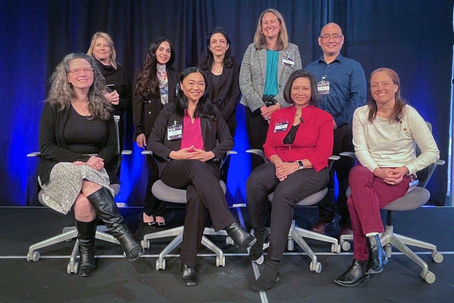
“I want to tell you that you don’t have to be just one thing,” said Katie Eckermann ’03, MEng ’04, director of business development at Advanced Micro Devices (AMD) at a networking event for students considering careers in hard technologies. “There is a huge wealth of different jobs and roles within the semiconductor industry.”
Eckermann was one of two keynote speakers at the Design the Solution conference, presented by the Global Semiconductor Alliance (GSA) Women’s Leadership Initiative, and c
“I want to tell you that you don’t have to be just one thing,” said Katie Eckermann ’03, MEng ’04, director of business development at Advanced Micro Devices (AMD) at a networking event for students considering careers in hard technologies. “There is a huge wealth of different jobs and roles within the semiconductor industry.”
Eckermann was one of two keynote speakers at the Design the Solution conference, presented by the Global Semiconductor Alliance (GSA)Women’s Leadership Initiative, and co-sponsored by MIT.nano. Following the speaking portion of the event, attendees were invited to meet with representatives from AMD, Analog Devices, Applied Materials, Arm, Cadence Design Systems, Cisco Systems, Intel, Marvell, Micron Technology, Samsung, Synopsys, and TSMC. This annual February event was one in a series organized by the GSA Women’s Leadership Initiative and hosted at universities across the country to highlight the global impact of a career in semiconductors and recruit more women into the hard-tech ecosystem.
Eckermann was joined by John Wuu ’96, MEng ’97, senior fellow design engineer at AMD. Together, the two highlighted some of the key trends and most significant challenges of the semiconductor industry, as well as shared their career paths and advice.
Wuu highlighted the tremendous increase in computing performance in recent years, illustrated in 2022 by Hewlett Packard’s Frontier computer — calculating complex problems much faster than several other supercomputers combined. While supercomputer performance has doubled every 1.2 years over the last 30 years, power efficiency has doubled only every 2.2 years — thus underscoring a clear need to continue the pace of performance sustainably and responsibly.
“These performance improvements are not about trying to break records just for the sake of breaking records,” said Wuu. “The demand for computing is very high and insatiable, and the improvements in performance that we’re getting are being used to solve some of humanity’s most challenging and important problems — from space exploration to climate change, and more.”
Both Wuu and Eckermann encouraged students pursuing careers in semiconductors to focus on learning and stretching themselves, taking risks, and growing their network. They also emphasized the many different skill sets needed in the semiconductor industry and the common problems that often exist across different market segments.
“One of the most valuable things about MIT is that it doesn’t teach you how to recite formulas or to memorize facts, it teaches you a framework on how to think,” said Eckermann. “And when it comes down to engineering, it’s all about solving complex problems.”
Following the keynote, Deb Dyson, senior staff engineering manager at Marvell, moderated a panel discussion featuring Rose Castanares, senior vice president for business management at TSMC North America; Kate Shamberger, field technical director for the Americas at Analog Devices; and Thy Tran, vice president of global frontend procurement at Micron Technology.
The panelists described their own individual and diverse career journeys, also emphasizing the tremendous amount and variety of opportunities currently available in semiconductors.
“Everywhere you look [in the semiconductor industry], it is the epicenter of all the intersectionality of the disciplines,” said Tran. “It’s the pure sciences, the math, the engineering, application-based, theory-based — I can’t believe I got so lucky to be in this arena.”
Some key themes of the panel discussion included the importance of teamwork and understanding the people you’re working with, the development of leadership styles, and trying out different types of roles within the industry. All speakers encouraged students to identify what they like to do most and think broadly and flexibly about how they can apply their skills and interests — and, above all, to always be learning and gaining a breadth of knowledge.
“It’s important to be continually learning — not just in your field, but also adjunct to your field,” said Castanares. “It’s not about trying to prove that you’re the smartest person in the room, but the most curious person in the room — and then apply and share that knowledge.”
At the Design the Solution conference co-sponsored by MIT.nano and the Global Semiconductor Association, MIT students received advice and networked with representatives from Advanced Micro Devices, Analog Devices, Applied Materials, Arm, Cadence, Cisco, Intel, Marvell, Micron, Samsung, and Synopsys.
The Northeast Microelectronics Internship Program (NMIP), an initiative of MIT’s Microsystems Technology Laboratories (MTL) to connect first- and second-year college students to careers in semiconductor and microelectronics industries, recently received a $75,000 grant to expand its reach and impact. The funding is part of $9.2 million in grants awarded by the Northeast Microelectronics Coalition (NEMC) Hub to boost technology advancement, workforce development, education, and student engagement
The Northeast Microelectronics Internship Program (NMIP), an initiative of MIT’s Microsystems Technology Laboratories (MTL) to connect first- and second-year college students to careers in semiconductor and microelectronics industries, recently received a $75,000 grant to expand its reach and impact. The funding is part of $9.2 million in grants awarded by the Northeast Microelectronics Coalition (NEMC) Hub to boost technology advancement, workforce development, education, and student engagement across the Northeast Region.
NMIP was founded by Tomás Palacios, the Clarence J. LeBel Professor of Electrical Engineering at MIT, and director of MTL. The grant, he says, will help address a significant barrier limiting the number of students who pursue careers in critical technological fields.
“Undergraduate students are key for the future of our nation’s microelectronics workforce. They directly fill important roles that require technical fluency or move on to advanced degrees,” says Palacios. “But these students have repeatedly shared with us that the lack of internships in their first few semesters in college is the main reason why many move to industries with a more established tradition of hiring undergraduate students in their early years. This program connects students and industry partners to fix this issue.”
The NMIP funding was announced on Jan. 30 during an event featuring Massachusetts Governor Maura Healey, Lt. Governor Kim Driscoll, and Economic Development Secretary Yvonne Hao, as well as leaders from the U.S. Department of Defense and the director of Microelectronics Commons at NSTXL, the National Security Technology Accelerator. The grant to support NMIP is part of $1.5 million in new workforce development grants aimed at spurring the microelectronics and semiconductor industry across the Northeast Region. The new awards are the first investments made by the NEMC Hub, a division of the Massachusetts Technology Collaborative, that is overseeing investments made by the federal CHIPS and Science Act following the formal establishment of the NEMC Hub in September 2023.
“We are very excited for the recognition the program is receiving. It is growing quickly and the support will help us further dive into our mission to connect talented students to the broader microelectronics ecosystem while integrating our values of curiosity, openness, excellence, respect, and community,” says Preetha Kingsview, who manages the program. “This grant will help us connect to the broader community convened by NEMC Hub in close collaboration with MassTech. We are very excited for what this support will help NMIP achieve.”
The funds provided by the NEMC Microelectronics Commons Hub will help expand the program more broadly across the Northeast, to support students and grow the pool of skilled workers for the microelectronics sector regionally. After receiving 300 applications in the first two years, the program received 296 applications in 2024 from students interested in summer internships, and is working with more than 25 industry partners across the Northeast. These NMIP students not only participate in industry-focused summer internships, but are also exposed to the broader microelectronics ecosystem through bi-weekly field trips to microelectronics companies in the region.
“The expansion of the program across the Northeast, and potentially nationwide, will extend the impact of this program to reach more students and benefit more microelectronics companies across the region,” says Christine Nolan, acting NEMC Hub program director. “Through hands-on training opportunities we are able to showcase the amazing jobs that exist in this sector and to strengthen the pipeline of talented workers to support the mission of the NEMC Hub and the national CHIPs investments.”
Sheila Wescott says her company, MACOM, a Lowell-based developer of semiconductor devices and components, is keenly interested in sourcing intern candidates from NMIP. “We already have a success story from this program,” she says. “One of our interns completed two summer programs with us and is continuing part time in the fall — and we anticipate him joining MACOM full time after graduation.”
“NMIP is an excellent platform to engage students with a diverse background and promote microelectronics technology,” says Bin Lu, CTO and co-founder of Finwave Semiconductor. “Finwave has benefited from engaging with the young engineers who are passionate about working with electronics and cutting-edge semiconductor technology. We are committed to continuing to work with NMIP.”
Massachusetts Governor Maura Healey speaks at the announcement of $9.2 million in new grants from the Northeast Microelectronics Coalition Hub. The governor was joined at the event by (left to right) Sally Kornbluth, president of MIT; Dev Shenoy, principal director for microelectronics for the Office of the Undersecretary for Defense; Kim Driscoll, lieutenant governor; Ben Linville-Engler, acting director of the NEMC Hub; and Carolyn Kirk, executive director of the MassTech Collaborative.
On August 6th, WT Microelectronics, a leading IC distributor based in Taiwan, held its investor conference where Chairman Simon Cheng expressed confidence that current semiconductor market headwinds are only a short-term phenomenon.
On August 6th, WT Microelectronics, a leading IC distributor based in Taiwan, held its investor conference where Chairman Simon Cheng expressed confidence that current semiconductor market headwinds are only a short-term phenomenon.
On August 6th, 2024, the Future of Memory and Storage (FMS) event commenced, highlighting AI storage applications and new products. Leading companies Phison and Western Digital (WD) have each made strides into the data center SSD market, both unveiling storage solutions with capacities reaching up to 64TB.
On August 6th, 2024, the Future of Memory and Storage (FMS) event commenced, highlighting AI storage applications and new products. Leading companies Phison and Western Digital (WD) have each made strides into the data center SSD market, both unveiling storage solutions with capacities reaching up to 64TB.
SEMICON Taiwan 2024 is set to take place from September 4-6 at the Taipei Nangang Exhibition Center, spotlighting key industry themes such as the AI value chain, advanced processes, heterogeneous integration, compound semiconductors, and silicon photonics.
SEMICON Taiwan 2024 is set to take place from September 4-6 at the Taipei Nangang Exhibition Center, spotlighting key industry themes such as the AI value chain, advanced processes, heterogeneous integration, compound semiconductors, and silicon photonics.
China-based foundries are rapidly expanding their capacity for mature logic IC processes, limiting local NOR production capability. As a result, global NOR flash supply and demand are close to equilibrium, with supply expected to be constrained in 2025, according to industry sources.
China-based foundries are rapidly expanding their capacity for mature logic IC processes, limiting local NOR production capability. As a result, global NOR flash supply and demand are close to equilibrium, with supply expected to be constrained in 2025, according to industry sources.
Samsung Electronics reported strong results for the second quarter of 2024, with its Device Solutions (DS) division, led by memory chips and the System LSI Business, driving nearly 60% of the company's operating profit.
Samsung Electronics reported strong results for the second quarter of 2024, with its Device Solutions (DS) division, led by memory chips and the System LSI Business, driving nearly 60% of the company's operating profit.
Taiwan Semiconductor Manufacturing Co. this week said its revenue for the second quarter 2024 reached $20.82 billion, making it the company's best quarter (at least in dollars) to date. TSMC's high-performance computing (HPC) platform revenue share exceeded 52% for the first time in many years due to demand for AI processors and rebound of the PC market.
TSMC earned $20.82 billion USD in revenue for the second quarter of 2024, a 32.8% year-over-year increase and a 10.3% increase from the previo
Taiwan Semiconductor Manufacturing Co. this week said its revenue for the second quarter 2024 reached $20.82 billion, making it the company's best quarter (at least in dollars) to date. TSMC's high-performance computing (HPC) platform revenue share exceeded 52% for the first time in many years due to demand for AI processors and rebound of the PC market.
TSMC earned $20.82 billion USD in revenue for the second quarter of 2024, a 32.8% year-over-year increase and a 10.3% increase from the previous quarter. Perhaps more remarkable, $20.82 billion is a higher result than the company posted Q3 2022 ($20.23 billion), the foundry's best quarter to date. Otherwise, in terms of profitability, TSMC booked $7.59 billion in net income for the quarter, for a gross margin of 53.2%. This is a decent bit off of TSMC's record margin of 60.4% (Q3'22), and comes as the company is still in the process of further ramping its N3 (3nm-class) fab lines.
When it comes to wafer revenue share, the company's N3 process technologies (3nm-class) accounted for 15% of wafer revenue in Q2 (up from 9% in the previous quarter), N5 production nodes (4nm and 5nm-classes) commanded 35% of TSMC's earnings in the second quarter (down from 37% in Q1 2024), and N7 fabrication processes (6nm and 7nm-classes) accounted for 17% of the foundry's wafer revenue in the second quarter of 2024 (down from 19% in Q1 2024). Advanced technologies all together (N3, N5, N7) accounted for 67% of total wafer revenue.
"Our business in the second quarter was supported by strong demand for our industry-leading 3nm and 5nm technologies, partially offset by continued smartphone seasonality," said Wendell Huang, Senior VP and Chief Financial Officer of TSMC. "Moving into third quarter 2024, we expect our business to be supported by strong smartphone and AI-related demand for our leading-edge process technologies."
TSMC usually starts ramping up production for Apple's fall products (e.g. iPhone) in the second quarter of the year, so it is not surprising that revenue share of N3 increased in Q2 of this year. Yet, keeping in mind that TSMC's revenue in general increased by 10.3% QoQ, the company's shipments of processors made on N5 and N7 nodes are showing resilience as demand for AI and HPC processors is high across the industry.
Speaking of TSMC's HPC sales, HPC platform sales accounted for 52% of TSMC's revenue for the first time in many years. The world's largest contract maker of chips produces many types of chips that get placed under the HPC umbrella, including AI processors, CPUs for client PCs, and system-on-chips (SoCs) for consoles, just to name a few. Yet, in this case TSMC attributes demand for AI processors as the main driver for its HPC success.
As for smartphone platform revenue, its share dropped to 33% as actual sales declined by 1% quarter-over-quarter. All other segments grew by 5% to 20%.
For the third quarter of 2024, TSMC expects revenue between US$22.4 billion and US$23.2 billion, with a gross profit margin of 53.5% to 55.5% and an operating profit margin of 42.5% to 44.5%. The company's sales are projected to be driven by strong demand for leading-edge process technologies as well as increased demand for AI and smartphones-related applications.
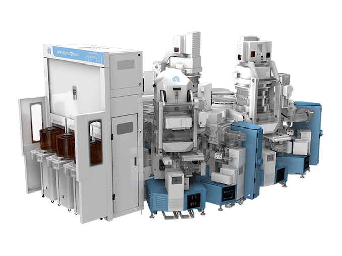
Although the pace of Moore's Law has undeniably slackened in the last decade, transistor density is still increasing with every new process technology. But there is a challenge with feeding power to smaller transistors, as with the smaller transistors comes thinner power wires within the chip, which increases their resistance and may cause yield loss. Looking to combat that effect, this week Applied Materials introduced its new Applied Endura Copper Barrier Seed IMS with Volta Ruthenium Copper V
Although the pace of Moore's Law has undeniably slackened in the last decade, transistor density is still increasing with every new process technology. But there is a challenge with feeding power to smaller transistors, as with the smaller transistors comes thinner power wires within the chip, which increases their resistance and may cause yield loss. Looking to combat that effect, this week Applied Materials introduced its new Applied Endura Copper Barrier Seed IMS with Volta Ruthenium Copper Vapor Deposition (CVD) tool, which enables chipmakers to keep using copper for wiring with 2 nm-class and more advanced process technologies.
Today's advanced logic processors have about 20 layers of metal, with thin signal wires and thicker power wires. Scaling down wiring with shrinking transistors presents numerous challenges. Thinner wires have higher electrical resistance, while closer wires heighten capacitance and electrical crosstalk. The combination of the two can lead to increased power consumption while also limiting performance scaling, which is particularly problematic for datacenter grade processors that are looking to have it all. Moving power rails to a wafer's back-side is expected to enhance performance and efficiency by reducing wiring complexity and freeing up space for more transistors.
But backside power delivery network (BSPDN) does not solve the problem with thin wires in general. As lithographic scaling progresses, both transistor features and wiring trenches become smaller. This reduction means that barriers and liners take up more space in these trenches, leaving insufficient room to deposit copper without creating voids, which raises resistance and can lower yields. Additionally, the closer proximity of wires thins the low-k dielectrics, making them more vulnerable to damage during the etching process. This damage increases capacitance and weakens the chips, making them unsuitable for 3D stacking. Consequently, as the industry advances, copper wiring faces significant physical scaling challenges. But Applied Materials has a solution.
Adopting Binary RuCo Liners
Contemporary manufacturing technologies use reflow to fill interconnects with copper, where anneals help the copper flow from the wafer surface into wiring trenches and vias. This process depends on the liners on which the copper flows. Normally, a CVD cobalt film was used for liners, but this film is too thick for 3nm-class nodes (which would affect resistance and yield).
Applied Materials proposes using a ruthenium cobalt (RuCo) binary liner with a thickness under 20A (2nm, 20 angstroms), which would provide better surface properties for copper reflow. This would ultimately allow for 33% more space for void-free conductive copper to be reflowed, reducing the overall resistance by 25%. While usage of the new liner requires new tooling, it can enable better interconnects that mean higher performance, lower power consumption and higher yields.
Applied Materials says that so far its new Endura Copper Barrier Seed IMS with Volta Ruthenium CVD tool has been adopted by all leading logic makers, including TSMC and Samsung Foundry for their 3nm-class nodes and beyond.
"The semiconductor industry must deliver dramatic improvements in energy-efficient performance to enable sustainable growth in AI computing," said Dr. Y.J. Mii, Executive Vice President and Co-Chief Operating Officer at TSMC. "New materials that reduce interconnect resistance will play an important role in the semiconductor industry, alongside other innovations to improve overall system performance and power."
New Low-K Dielectric
But thin and efficient liner is not the only thing crucial for wiring at 3nm production nodes and beyond. Trenches for wiring are filed not only with a Co/RuCo liner and a Ta/N barrier, but with low dielectric constant (Low-K) film to minimize electrical charge buildup, reduce power consumption, and lower signal interference. Applied Materials has offered its Black Diamond Low-K film since the early 2000s.
But new production nodes require better dielectrics, so this week the company introduced an upgraded version of Black Diamond material and a plasma-enhanced chemical vapor deposition (PEVCD) tool to apply it, the Producer Black Diamond PECVD series. This new material allows for scaling down to 2nm and beyond by further reducing the dielectric constant while also increasing the mechanical strength of the chips, which is good for 3D stacking both for logic and memory. The new Black Diamond is being rapidly adopted by major logic and DRAM chipmakers, Applied says.
"The AI era needs more energy-efficient computing, and chip wiring and stacking are critical to performance and power consumption," said Dr. Prabu Raja, President of the Semiconductor Products Group at Applied Materials. "Applied's newest integrated materials solution enables the industry to scale low-resistance copper wiring to the emerging angstrom nodes, while our latest low-k dielectric material simultaneously reduces capacitance and strengthens chips to take 3D stacking to new heights."
MediaTek, the leading smartphone AP supplier in India, sees the country as a promising market for its automotive technology. The company is focusing on providing scalable hardware and software solutions while prioritizing safety and reliability for the automotive sector.
MediaTek, the leading smartphone AP supplier in India, sees the country as a promising market for its automotive technology. The company is focusing on providing scalable hardware and software solutions while prioritizing safety and reliability for the automotive sector.
Indian opto-semiconductor supplier Polymatech has announced the acquisition of a US-based semiconductor equipment provider specializing in packaging and testing. This move is part of Polymatech's broader strategy to build an integrated chipmaking business that spans multiple sectors.
Indian opto-semiconductor supplier Polymatech has announced the acquisition of a US-based semiconductor equipment provider specializing in packaging and testing. This move is part of Polymatech's broader strategy to build an integrated chipmaking business that spans multiple sectors.
South Korea's leading component suppliers, Samsung Electro-Mechanics (Semco) and LG Innotek, have defied the traditional second-quarter slump with impressive results, driven by recovering market demand and a strategic focus on high-value products. As they head into the peak season of the second half, both companies are poised to expand their high-margin product lines to fuel further growth.
South Korea's leading component suppliers, Samsung Electro-Mechanics (Semco) and LG Innotek, have defied the traditional second-quarter slump with impressive results, driven by recovering market demand and a strategic focus on high-value products. As they head into the peak season of the second half, both companies are poised to expand their high-margin product lines to fuel further growth.
Worldwide silicon wafer shipments increased 7.1% quarter-on-quarter to 3.035 billion square inches in the second quarter of 2024, but saw an 8.9% decline from the 3.33 billion square inches recorded during the same quarter last year, SEMI disclosed in its quarterly analysis of the silicon wafer industry.
Worldwide silicon wafer shipments increased 7.1% quarter-on-quarter to 3.035 billion square inches in the second quarter of 2024, but saw an 8.9% decline from the 3.33 billion square inches recorded during the same quarter last year, SEMI disclosed in its quarterly analysis of the silicon wafer industry.
The current hypergrowth in GPUs and other accelerator chips for AI in the cloud and the data center will eventually decelerate but not until it has transformed the industry, according to Omdia. The market will ultimately reach US$151 billion in 2029, having grown from just under US$10 billion in 2022 to US$78 billion this year.
The current hypergrowth in GPUs and other accelerator chips for AI in the cloud and the data center will eventually decelerate but not until it has transformed the industry, according to Omdia. The market will ultimately reach US$151 billion in 2029, having grown from just under US$10 billion in 2022 to US$78 billion this year.
Following a 37% surge in sales during the off-season second quarter, PCB giant Zhen Ding reported robust performance in July. The company anticipates strong demand momentum across its four key business areas for the second half of the year.
Following a 37% surge in sales during the off-season second quarter, PCB giant Zhen Ding reported robust performance in July. The company anticipates strong demand momentum across its four key business areas for the second half of the year.
Infineon Technologies has completed the sale of its two backend manufacturing sites, one in Cavite, Philippines, and one in Cheonan, South Korea, to two fully owned subsidiaries of ASE, a Taiwan-based provider of independent semiconductor manufacturing services in assembly and test, according to the semiconductor IDM company.
Infineon Technologies has completed the sale of its two backend manufacturing sites, one in Cavite, Philippines, and one in Cheonan, South Korea, to two fully owned subsidiaries of ASE, a Taiwan-based provider of independent semiconductor manufacturing services in assembly and test, according to the semiconductor IDM company.
Innolux has selected FOPLP as the primary driver of its transformation from an LCD panel maker to a semiconductor firm and is getting ready for market growth, according to company chairman Jim Hung.
Innolux has selected FOPLP as the primary driver of its transformation from an LCD panel maker to a semiconductor firm and is getting ready for market growth, according to company chairman Jim Hung.
MediaTek is confident in the stability and resilience of its ASIC business between 2025 and 2028 and is committed to bolstering the ecosystems of related industries, according to the Taiwanese IC design house.
MediaTek is confident in the stability and resilience of its ASIC business between 2025 and 2028 and is committed to bolstering the ecosystems of related industries, according to the Taiwanese IC design house.
Taiwanese PCB makers have particularly targeted the automotive market in their investments. The simultaneous expansion of their operations in Thailand reflects their clients' emphasis on a "China+1" production strategy. Furthermore, the Thai government's focus on electric vehicles (EVs) as a priority industry has attracted companies from Taiwan, South Korea, Japan, and China to expand production in the country.
Taiwanese PCB makers have particularly targeted the automotive market in their investments. The simultaneous expansion of their operations in Thailand reflects their clients' emphasis on a "China+1" production strategy. Furthermore, the Thai government's focus on electric vehicles (EVs) as a priority industry has attracted companies from Taiwan, South Korea, Japan, and China to expand production in the country.
Taiwan's chipmaking tool exports, which prioritize the market in China, have been impacted by China's increased efforts to achieve self-sufficiency in semiconductor equipment.
Taiwan's chipmaking tool exports, which prioritize the market in China, have been impacted by China's increased efforts to achieve self-sufficiency in semiconductor equipment.
TSMC has notified clients of a 3-8% price increase for its 5nm and 3nm process manufacturing in 2025 to reflect escalating costs, according to sources at IC design houses.
TSMC has notified clients of a 3-8% price increase for its 5nm and 3nm process manufacturing in 2025 to reflect escalating costs, according to sources at IC design houses.
Infineon Technologies AG reported revenue that missed analysts' expectations after the hoped-for resurgence in the electric vehicle market was delayed.
Infineon Technologies AG reported revenue that missed analysts' expectations after the hoped-for resurgence in the electric vehicle market was delayed.
Winbond Electronics, a specialty DRAM and flash memory chipmaker, has begun ramping up its DDR4 chip output in the second half of 2024, with the memory output increase expected to boost its sales performance.
Winbond Electronics, a specialty DRAM and flash memory chipmaker, has begun ramping up its DDR4 chip output in the second half of 2024, with the memory output increase expected to boost its sales performance.
Over the past two years, the semiconductor industry has undergone a dramatic transformation, shifting its focus to AI development. This shift has driven chipmakers to significantly reallocate resources, diverting investments from consumer applications to AI computing and encouraging employees to transition into AI-related roles.
Over the past two years, the semiconductor industry has undergone a dramatic transformation, shifting its focus to AI development. This shift has driven chipmakers to significantly reallocate resources, diverting investments from consumer applications to AI computing and encouraging employees to transition into AI-related roles.
Huawei reportedly mimics Apple by designing a chip with shared memory to improve its chip performance amid US sanctions and develop its in-house chip infrastructure ecosystem.
Huawei reportedly mimics Apple by designing a chip with shared memory to improve its chip performance amid US sanctions and develop its in-house chip infrastructure ecosystem.
Kioxia has announced that the construction of Fab2 (K2) at its factory site in Kitakami was completed in July. K2 is the second flash memory manufacturing facility at Kioxia's Kitakami site in Iwate Prefecture, Japan.
Kioxia has announced that the construction of Fab2 (K2) at its factory site in Kitakami was completed in July. K2 is the second flash memory manufacturing facility at Kioxia's Kitakami site in Iwate Prefecture, Japan.
Kitakami Plant (K2 is on the left, K1 is on the right). Credit: Kioxia
Without a map, it can be just about impossible to know not just where you are, but where you’re going, and that’s especially true when it comes to materials properties.
For decades, scientists have understood that while bulk materials behave in certain ways, those rules can break down for materials at the micro- and nano-scales, and often in surprising ways. One of those surprises was the finding that, for some materials, applying even modest strains — a concept known as elastic strain engineer
Without a map, it can be just about impossible to know not just where you are, but where you’re going, and that’s especially true when it comes to materials properties.
For decades, scientists have understood that while bulk materials behave in certain ways, those rules can break down for materials at the micro- and nano-scales, and often in surprising ways. One of those surprises was the finding that, for some materials, applying even modest strains — a concept known as elastic strain engineering — on materials can dramatically improve certain properties, provided those strains stay elastic and do not relax away by plasticity, fracture, or phase transformations. Micro- and nano-scale materials are especially good at holding applied strains in the elastic form.
Precisely how to apply those elastic strains (or equivalently, residual stress) to achieve certain material properties, however, had been less clear — until recently.
Using a combination of first principles calculations and machine learning, a team of MIT researchers has developed the first-ever map of how to tune crystalline materials to produce specific thermal and electronic properties.
Led by Ju Li, the Battelle Energy Alliance Professor in Nuclear Engineering and professor of materials science and engineering, the team described a framework for understanding precisely how changing the elastic strains on a material can fine-tune properties like thermal and electrical conductivity. The work is described in an open-access paper published in PNAS.
“For the first time, by using machine learning, we’ve been able to delineate the complete six-dimensional boundary of ideal strength, which is the upper limit to elastic strain engineering, and create a map for these electronic and phononic properties,” Li says. “We can now use this approach to explore many other materials. Traditionally, people create new materials by changing the chemistry.”
“For example, with a ternary alloy, you can change the percentage of two elements, so you have two degrees of freedom,” he continues. “What we’ve shown is that diamond, with just one element, is equivalent to a six-component alloy, because you have six degrees of elastic strain freedom you can tune independently.”
Small strains, big material benefits
The paper builds on a foundation laid as far back as the 1980s, when researchers first discovered that the performance of semiconductor materials doubled when a small — just 1 percent — elastic strain was applied to the material.
While that discovery was quickly commercialized by the semiconductor industry and today is used to increase the performance of microchips in everything from laptops to cellphones, that level of strain is very small compared to what we can achieve now, says Subra Suresh, the Vannevar Bush Professor of Engineering Emeritus.
In a 2018 Science paper, Suresh, Dao, and colleagues demonstrated that 1 percent strain was just the tip of the iceberg.
As part of a 2018 study, Suresh and colleagues demonstrated for the first time that diamond nanoneedles could withstand elastic strains of as much as 9 percent and still return to their original state. Later on, several groups independently confirmed that microscale diamond can indeed elastically deform by approximately 7 percent in tension reversibly.
“Once we showed we could bend nanoscale diamonds and create strains on the order of 9 or 10 percent, the question was, what do you do with it,” Suresh says. “It turns out diamond is a very good semiconductor material … and one of our questions was, if we can mechanically strain diamond, can we reduce the band gap from 5.6 electron-volts to two or three? Or can we get it all the way down to zero, where it begins to conduct like a metal?”
To answer those questions, the team first turned to machine learning in an effort to get a more precise picture of exactly how strain altered material properties.
“Strain is a big space,” Li explains. “You can have tensile strain, you can have shear strain in multiple directions, so it’s a six-dimensional space, and the phonon band is three-dimensional, so in total there are nine tunable parameters. So, we’re using machine learning, for the first time, to create a complete map for navigating the electronic and phononic properties and identify the boundaries.”
Armed with that map, the team subsequently demonstrated how strain could be used to dramatically alter diamond’s semiconductor properties.
“Diamond is like the Mt. Everest of electronic materials,” Li says, “because it has very high thermal conductivity, very high dielectric breakdown strengths, a very big carrier mobility. What we have shown is we can controllably squish Mt. Everest down … so we show that by strain engineering you can either improve diamond’s thermal conductivity by a factor of two, or make it much worse by a factor of 20.”
New map, new applications
Going forward, the findings could be used to explore a host of exotic material properties, Li says, from dramatically reduced thermal conductivity to superconductivity.
“Experimentally, these properties are already accessible with nanoneedles and even microbridges,” he says. “And we have seen exotic properties, like reducing diamond’s (thermal conductivity) to only a few hundred watts per meter-Kelvin. Recently, people have shown that you can produce room-temperature superconductors with hydrides if you squeeze them to a few hundred gigapascals, so we have found all kinds of exotic behavior once we have the map.”
The results could also influence the design of next-generation computer chips capable of running much faster and cooler than today’s processors, as well as quantum sensors and communication devices. As the semiconductor manufacturing industry moves to denser and denser architectures, Suresh says the ability to tune a material’s thermal conductivity will be particularly important for heat dissipation.
While the paper could inform the design of future generations of microchips, Zhe Shi, a postdoc in Li’s lab and first author of the paper, says more work will be needed before those chips find their way into the average laptop or cellphone.
“We know that 1 percent strain can give you an order of magnitude increase in the clock speed of your CPU,” Shi says. “There are a lot of manufacturing and device problems that need to be solved in order for this to become realistic, but I think it’s definitely a great start. It’s an exciting beginning to what could lead to significant strides in technology.”
This work was supported with funding from the Defense Threat Reduction Agency, an NSF Graduate Research Fellowship, the Nanyang Technological University School of Biological Sciences, the National Science Foundation (NSF), the MIT Vannevar Bush Professorship, and a Nanyang Technological University Distinguished University Professorship.
The “map,” or the phonon stability boundary, is a graphical representation that plots the stability regions of a crystal as a function of strain. This map helps scientists and engineers determine the conditions under which a material can exist in a particular phase and when it might fail or transition to another phase. By analyzing the phonon stability boundary, researchers can understand material properties at extreme conditions and design new materials with desired characteristics.
“I want to tell you that you don’t have to be just one thing,” said Katie Eckermann ’03, MEng ’04, director of business development at Advanced Micro Devices (AMD) at a networking event for students considering careers in hard technologies. “There is a huge wealth of different jobs and roles within the semiconductor industry.”
Eckermann was one of two keynote speakers at the Design the Solution conference, presented by the Global Semiconductor Alliance (GSA) Women’s Leadership Initiative, and c
“I want to tell you that you don’t have to be just one thing,” said Katie Eckermann ’03, MEng ’04, director of business development at Advanced Micro Devices (AMD) at a networking event for students considering careers in hard technologies. “There is a huge wealth of different jobs and roles within the semiconductor industry.”
Eckermann was one of two keynote speakers at the Design the Solution conference, presented by the Global Semiconductor Alliance (GSA)Women’s Leadership Initiative, and co-sponsored by MIT.nano. Following the speaking portion of the event, attendees were invited to meet with representatives from AMD, Analog Devices, Applied Materials, Arm, Cadence Design Systems, Cisco Systems, Intel, Marvell, Micron Technology, Samsung, Synopsys, and TSMC. This annual February event was one in a series organized by the GSA Women’s Leadership Initiative and hosted at universities across the country to highlight the global impact of a career in semiconductors and recruit more women into the hard-tech ecosystem.
Eckermann was joined by John Wuu ’96, MEng ’97, senior fellow design engineer at AMD. Together, the two highlighted some of the key trends and most significant challenges of the semiconductor industry, as well as shared their career paths and advice.
Wuu highlighted the tremendous increase in computing performance in recent years, illustrated in 2022 by Hewlett Packard’s Frontier computer — calculating complex problems much faster than several other supercomputers combined. While supercomputer performance has doubled every 1.2 years over the last 30 years, power efficiency has doubled only every 2.2 years — thus underscoring a clear need to continue the pace of performance sustainably and responsibly.
“These performance improvements are not about trying to break records just for the sake of breaking records,” said Wuu. “The demand for computing is very high and insatiable, and the improvements in performance that we’re getting are being used to solve some of humanity’s most challenging and important problems — from space exploration to climate change, and more.”
Both Wuu and Eckermann encouraged students pursuing careers in semiconductors to focus on learning and stretching themselves, taking risks, and growing their network. They also emphasized the many different skill sets needed in the semiconductor industry and the common problems that often exist across different market segments.
“One of the most valuable things about MIT is that it doesn’t teach you how to recite formulas or to memorize facts, it teaches you a framework on how to think,” said Eckermann. “And when it comes down to engineering, it’s all about solving complex problems.”
Following the keynote, Deb Dyson, senior staff engineering manager at Marvell, moderated a panel discussion featuring Rose Castanares, senior vice president for business management at TSMC North America; Kate Shamberger, field technical director for the Americas at Analog Devices; and Thy Tran, vice president of global frontend procurement at Micron Technology.
The panelists described their own individual and diverse career journeys, also emphasizing the tremendous amount and variety of opportunities currently available in semiconductors.
“Everywhere you look [in the semiconductor industry], it is the epicenter of all the intersectionality of the disciplines,” said Tran. “It’s the pure sciences, the math, the engineering, application-based, theory-based — I can’t believe I got so lucky to be in this arena.”
Some key themes of the panel discussion included the importance of teamwork and understanding the people you’re working with, the development of leadership styles, and trying out different types of roles within the industry. All speakers encouraged students to identify what they like to do most and think broadly and flexibly about how they can apply their skills and interests — and, above all, to always be learning and gaining a breadth of knowledge.
“It’s important to be continually learning — not just in your field, but also adjunct to your field,” said Castanares. “It’s not about trying to prove that you’re the smartest person in the room, but the most curious person in the room — and then apply and share that knowledge.”
At the Design the Solution conference co-sponsored by MIT.nano and the Global Semiconductor Association, MIT students received advice and networked with representatives from Advanced Micro Devices, Analog Devices, Applied Materials, Arm, Cadence, Cisco, Intel, Marvell, Micron, Samsung, and Synopsys.