Physicists create five-lane superhighway for electrons
MIT physicists and colleagues have created a five-lane superhighway for electrons that could allow ultra-efficient electronics and more.
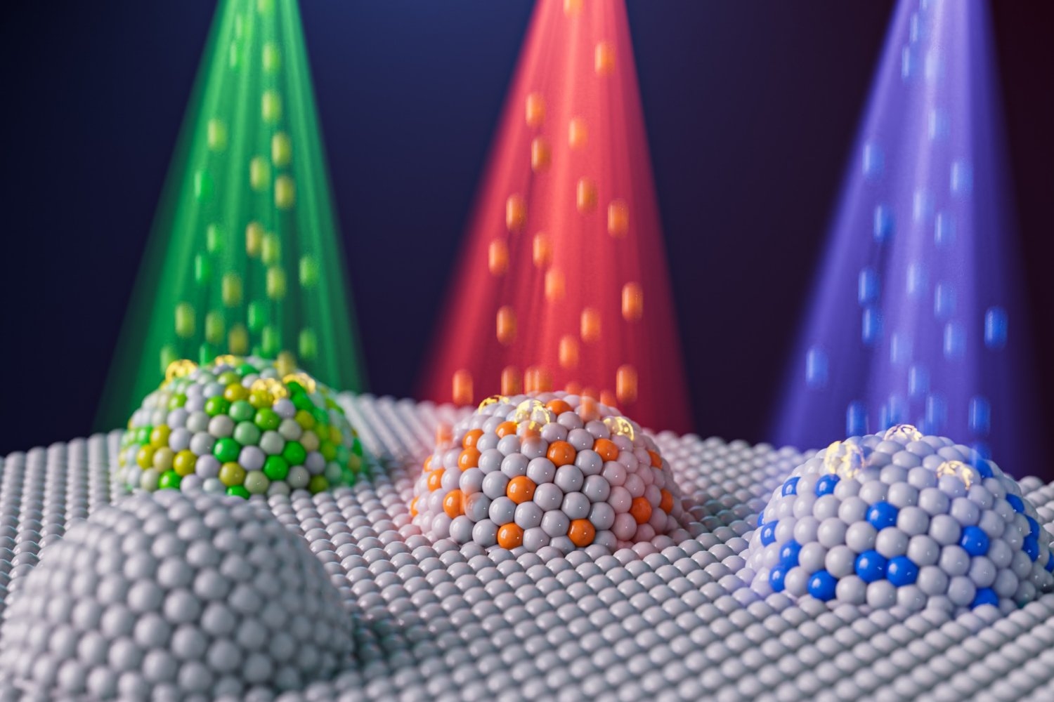
The work, reported in the May 10 issue of Science, is one of several important discoveries by the same team over the past year involving a material that is a unique form of graphene.
“This discovery has direct implications for low-power electronic devices because no energy is lost during the propagation of electrons, which is not the case in regular materials where the electrons are scattered,” says Long Ju, an assistant professor in the Department of Physics and corresponding author of the Science paper.
The phenomenon is akin to cars traveling down an open turnpike as opposed to those moving through neighborhoods. The neighborhood cars can be stopped or slowed by other drivers making abrupt stops or U-turns that disrupt an otherwise smooth commute.
A new material
The material behind this work, known as rhombohedral pentalayer graphene, was discovered two years ago by physicists led by Ju. “We found a goldmine, and every scoop is revealing something new,” says Ju, who is also affiliated with MIT’s Materials Research Laboratory.
In a Nature Nanotechnology paper last October, Ju and colleagues reported the discovery of three important properties arising from rhombohedral graphene. For example, they showed that it could be topological, or allow the unimpeded movement of electrons around the edge of the material but not through the middle. That resulted in a superhighway, but required the application of a large magnetic field some tens of thousands times stronger than the Earth’s magnetic field.
In the current work, the team reports creating the superhighway without any magnetic field.
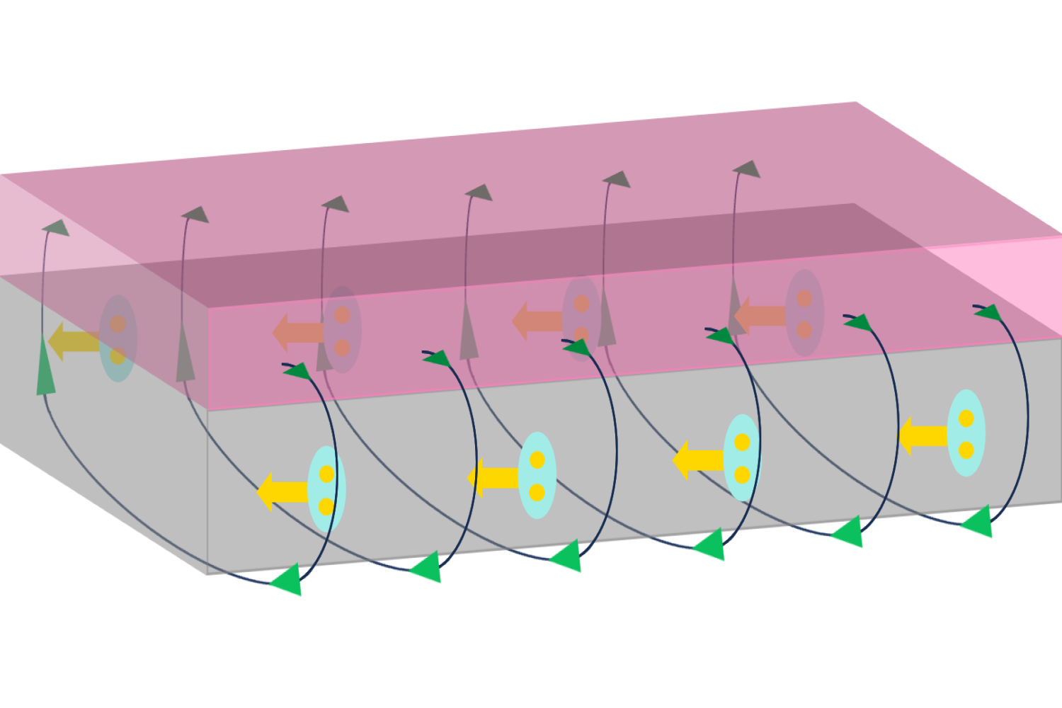
Tonghang Han, an MIT graduate student in physics, is a co-first author of the paper. “We are not the first to discover this general phenomenon, but we did so in a very different system. And compared to previous systems, ours is simpler and also supports more electron channels.” Explains Ju, “other materials can only support one lane of traffic on the edge of the material. We suddenly bumped it up to five.”
Additional co-first authors of the paper who contributed equally to the work are Zhengguang Lu and Yuxuan Yao. Lu is a postdoc in the Materials Research Laboratory. Yao conducted the work as a visiting undergraduate student from Tsinghua University. Other authors are MIT professor of physics Liang Fu; Jixiang Yang and Junseok Seo, both MIT graduate students in physics; Chiho Yoon and Fan Zhang of the University of Texas at Dallas; and Kenji Watanabe and Takashi Taniguchi of the National Institute for Materials Science in Japan.
How it works
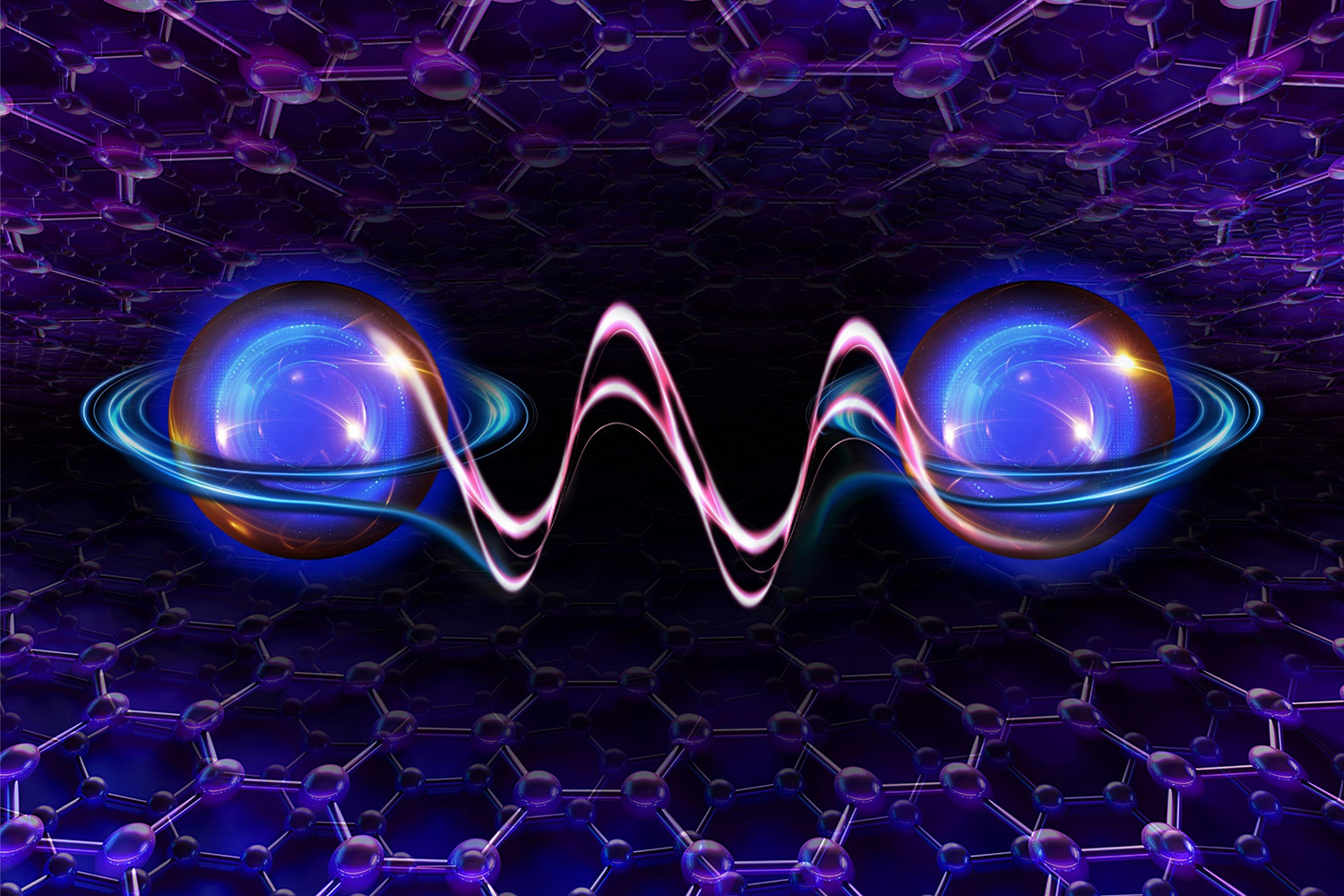
Graphite, the primary component of pencil lead, is composed of many layers of graphene, a single layer of carbon atoms arranged in hexagons resembling a honeycomb structure. Rhombohedral graphene is composed of five layers of graphene stacked in a specific overlapping order.
Ju and colleagues isolated rhombohedral graphene thanks to a novel microscope Ju built at MIT in 2021 that can quickly and relatively inexpensively determine a variety of important characteristics of a material at the nanoscale. Pentalayer rhombohedral stacked graphene is only a few billionths of a meter thick.
In the current work, the team tinkered with the original system, adding a layer of tungsten disulfide (WS2). “The interaction between the WS2 and the pentalayer rhombohedral graphene resulted in this five-lane superhighway that operates at zero magnetic field,” says Ju.
Comparison to superconductivity
The phenomenon that the Ju group discovered in rhombohedral graphene that allows electrons to travel with no resistance at zero magnetic field is known as the quantum anomalous Hall effect. Most people are more familiar with superconductivity, a completely different phenomenon that does the same thing but happens in very different materials.
Ju notes that although superconductors were discovered in the 1910s, it took some 100 years of research to coax the system to work at the higher temperatures necessary for applications. “And the world record is still well below room temperature,” he notes.
Similarly, the rhombohedral graphene superhighway currently operates at about 2 kelvins, or -456 degrees Fahrenheit. “It will take a lot of effort to elevate the temperature, but as physicists, our job is to provide the insight; a different way for realizing this [phenomenon],” Ju says.
Very exciting
The discoveries involving rhombohedral graphene came as a result of painstaking research that wasn’t guaranteed to work. “We tried many recipes over many months,” says Han, “so it was very exciting when we cooled the system to a very low temperature and [a five-lane superhighway operating at zero magnetic field] just popped out.”
Says Ju, “it’s very exciting to be the first to discover a phenomenon in a new system, especially in a material that we uncovered.”
This work was supported by a Sloan Fellowship; the U.S. National Science Foundation; the U.S. Office of the Under Secretary of Defense for Research and Engineering; the Japan Society for the Promotion of Science KAKENHI; and the World Premier International Research Initiative of Japan.
![]()
© Image: Sampson Wilcox/Research Laboratory of Electronics