Scientists observe record-setting electron mobility in a new crystal film
A material with a high electron mobility is like a highway without traffic. Any electrons that flow into the material experience a commuter’s dream, breezing through without any obstacles or congestion to slow or scatter them off their path.
The higher a material’s electron mobility, the more efficient its electrical conductivity, and the less energy is lost or wasted as electrons zip through. Advanced materials that exhibit high electron mobility will be essential for more efficient and sustainable electronic devices that can do more work with less power.
Now, physicists at MIT, the Army Research Lab, and elsewhere have achieved a record-setting level of electron mobility in a thin film of ternary tetradymite — a class of mineral that is naturally found in deep hydrothermal deposits of gold and quartz.
For this study, the scientists grew pure, ultrathin films of the material, in a way that minimized defects in its crystalline structure. They found that this nearly perfect film — much thinner than a human hair — exhibits the highest electron mobility in its class.
The team was able to estimate the material’s electron mobility by detecting quantum oscillations when electric current passes through. These oscillations are a signature of the quantum mechanical behavior of electrons in a material. The researchers detected a particular rhythm of oscillations that is characteristic of high electron mobility — higher than any ternary thin films of this class to date.
“Before, what people had achieved in terms of electron mobility in these systems was like traffic on a road under construction — you’re backed up, you can’t drive, it’s dusty, and it’s a mess,” says Jagadeesh Moodera, a senior research scientist in MIT’s Department of Physics. “In this newly optimized material, it’s like driving on the Mass Pike with no traffic.”
The team’s results, which appear today in the journal Materials Today Physics, point to ternary tetradymite thin films as a promising material for future electronics, such as wearable thermoelectric devices that efficiently convert waste heat into electricity. (Tetradymites are the active materials that cause the cooling effect in commercial thermoelectric coolers.) The material could also be the basis for spintronic devices, which process information using an electron’s spin, using far less power than conventional silicon-based devices.
The study also uses quantum oscillations as a highly effective tool for measuring a material’s electronic performance.
“We are using this oscillation as a rapid test kit,” says study author Hang Chi, a former research scientist at MIT who is now at the University of Ottawa. “By studying this delicate quantum dance of electrons, scientists can start to understand and identify new materials for the next generation of technologies that will power our world.”
Chi and Moodera’s co-authors include Patrick Taylor, formerly of MIT Lincoln Laboratory, along with Owen Vail and Harry Hier of the Army Research Lab, and Brandi Wooten and Joseph Heremans of Ohio State University.
Beam down
The name “tetradymite” derives from the Greek “tetra” for “four,” and “dymite,” meaning “twin.” Both terms describe the mineral’s crystal structure, which consists of rhombohedral crystals that are “twinned” in groups of four — i.e. they have identical crystal structures that share a side.
Tetradymites comprise combinations of bismuth, antimony tellurium, sulfur, and selenium. In the 1950s, scientists found that tetradymites exhibit semiconducting properties that could be ideal for thermoelectric applications: The mineral in its bulk crystal form was able to passively convert heat into electricity.
Then, in the 1990s, the late Institute Professor Mildred Dresselhaus proposed that the mineral’s thermoelectric properties might be significantly enhanced, not in its bulk form but within its microscopic, nanometer-scale surface, where the interactions of electrons is more pronounced. (Heremans happened to work in Dresselhaus’ group at the time.)
“It became clear that when you look at this material long enough and close enough, new things will happen,” Chi says. “This material was identified as a topological insulator, where scientists could see very interesting phenomena on their surface. But to keep uncovering new things, we have to master the material growth.”
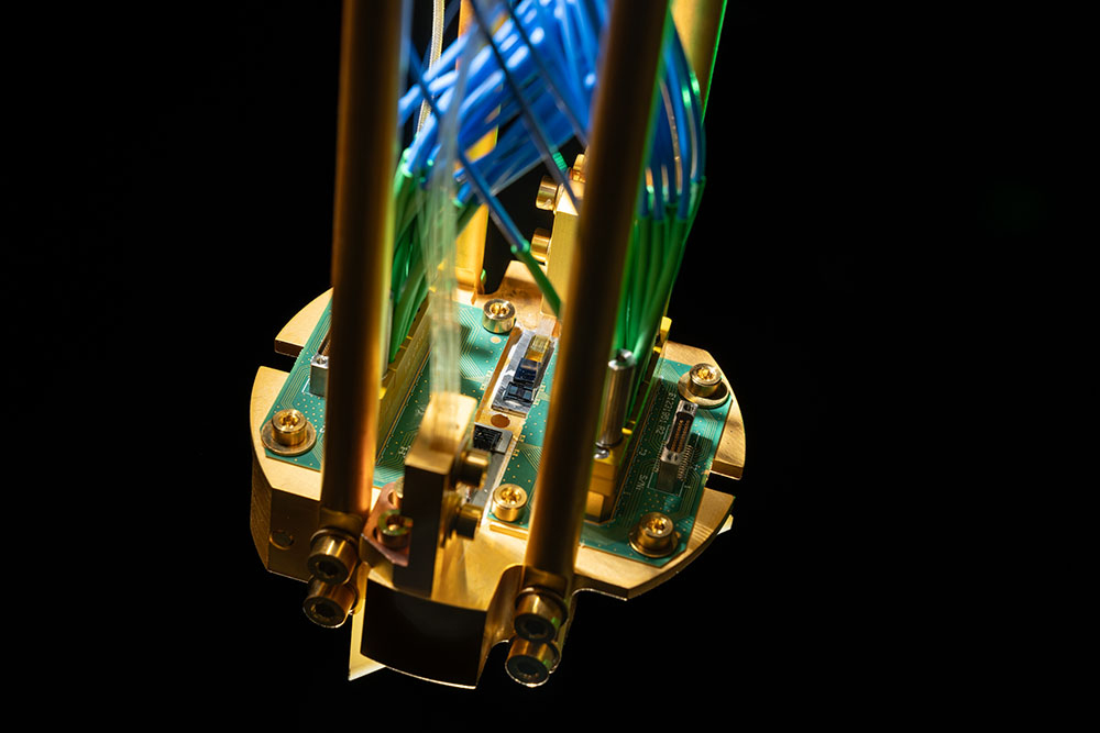
To grow thin films of pure crystal, the researchers employed molecular beam epitaxy — a method by which a beam of molecules is fired at a substrate, typically in a vacuum, and with precisely controlled temperatures. When the molecules deposit on the substrate, they condense and build up slowly, one atomic layer at a time. By controlling the timing and type of molecules deposited, scientists can grow ultrathin crystal films in exact configurations, with few if any defects.
“Normally, bismuth and tellurium can interchange their position, which creates defects in the crystal,” co-author Taylor explains. “The system we used to grow these films came down with me from MIT Lincoln Laboratory, where we use high purity materials to minimize impurities to undetectable limits. It is the perfect tool to explore this research.”
Free flow
The team grew thin films of ternary tetradymite, each about 100 nanometers thin. They then tested the film’s electronic properties by looking for Shubnikov-de Haas quantum oscillations — a phenomenon that was discovered by physicists Lev Shubnikov and Wander de Haas, who found that a material’s electrical conductivity can oscillate when exposed to a strong magnetic field at low temperatures. This effect occurs because the material’s electrons fill up specific energy levels that shift as the magnetic field changes.
Such quantum oscillations could serve as a signature of a material’s electronic structure, and the ways in which electrons behave and interact. Most notably for the MIT team, the oscillations could determine a material’s electron mobility: If oscillations exist, it must mean that the material’s electrical resistance is able to change, and by inference, electrons can be mobile, and made to easily flow.
The team looked for signs of quantum oscillations in their new films, by first exposing them to ultracold temperatures and a strong magnetic field, then running an electric current through the film and measuring the voltage along its path, as they tuned the magnetic field up and down.
“It turns out, to our great joy and excitement, that the material’s electrical resistance oscillates,” Chi says. “Immediately, that tells you that this has very high electron mobility.”
Specifically, the team estimates that the ternary tetradymite thin film exhibits an electron mobility of 10,000 cm2/V-s — the highest mobility of any ternary tetradymite film yet measured. The team suspects that the film’s record mobility has something to do with its low defects and impurities, which they were able to minimize with their precise growth strategies. The fewer a material’s defects, the fewer obstacles an electron encounters, and the more freely it can flow.
“This is showing it’s possible to go a giant step further, when properly controlling these complex systems,” Moodera says. “This tells us we’re in the right direction, and we have the right system to proceed further, to keep perfecting this material down to even much thinner films and proximity coupling for use in future spintronics and wearable thermoelectric devices.”
This research was supported in part by the Army Research Office, National Science Foundation, Office of Naval Research, Canada Research Chairs Program and Natural Sciences and Engineering Research Council of Canada.
![]()
© Credit: Courtesy of the researchers; edited by MIT News