FreshRSS

Normální zobrazení

Jsou dostupné nové články, klikněte pro obnovení stránky.
PředevčíremSemiconductor Engineering
  • ✇Semiconductor Engineering
  • Intel, And Others, InsideEd Sperling
    Intel this week made a strong case for how it will regain global process technology leadership, unfurling an aggressive technology and business roadmap that includes everything from several more process node shrinks that ultimately could scale into the single-digit angstrom range to a broad shift in how it approaches the market. Both will be essential for processing the huge amount of data for AI everywhere, and to win back some of the market share that NVIDIA currently wields. Intel’s strategy
     

Intel, And Others, Inside

22. Únor 2024 v 09:30

Intel this week made a strong case for how it will regain global process technology leadership, unfurling an aggressive technology and business roadmap that includes everything from several more process node shrinks that ultimately could scale into the single-digit angstrom range to a broad shift in how it approaches the market. Both will be essential for processing the huge amount of data for AI everywhere, and to win back some of the market share that NVIDIA currently wields.

Intel’s strategy is many layers thick. It includes a long list of innovations, including backside power delivery, which significantly reduces congestion and noise in more than a dozen metal layers, to 2.5D and 3D-ICs using a standard architecture for internally developed and third-party chiplets and IP. And it encompasses everything from a broad and open ecosystem — a sharp departure from its past own-it-all strategy, which once prompted anti-competitive charges — as well as a willingness to work more closely with customers, competitors, and governments to achieve its goals.

Whether Intel delivers on that promise remains to be seen. But the breadth of its vision, particularly for Intel Foundry, and the ambitious delivery schedule represent a sharp change in direction and culture for the 56-year-old chipmaker.

Of particular note is how the companies internal silos are being deconstructed. Intel CEO Pat Gelsinger said there will be a clean line between Intel products and Intel Foundry, but noted the foundry will be offer Intel developments and innovations developed by the product teams. “The à la carte menu is wide open for the industry,” he said during a Q&A session. “Clearwater Forest, which I showed today, is a construct that was innovated by my Xeon team — how to do hybrid bonding, Intel three base dies, 18A top die, being able to solve a lot of the CoWoS/Foveros problems using EMIB and hybrid bonding. That will become a set of collaterals that will benefit the foundry. They’re going to sell that constructional opportunity as a better way to build AI chips. So clearly, I’m taking product group intellectual property and leveraging it on the foundry side.”

This may sound like business as usual for a foundry, but Intel for years waffled over its commitment to a foundry model. In fact, it was viewed as an IDM that only began selling wafers to customers as the cost of maintaining its own fab began to skyrocket out of country. Creating separation between the two is a fundamental shift, and it’s an essential one for building trust in a complex world of sometimes partners, sometimes competitors. In the past, the company closely guarded its IP, confining that to its own processors rather than unbundling it and selling it to potential competitors. With this new division, Intel potentially can generate profits both from customized chips that leverage technologies it develops internally for other applications, as well as its own chip business.

Gelsinger is adamant about this being a leading-edge technology company, not a supplier of all components required in systems. “I’m not going to solve 200mm supply chain issues,” he said. “And, by the way, there are not going to be more 200mm factories built, for the most part, outside of specialty like SiC. There are some crazy discussions, like when some Europeans say, ‘I don’t need a leading-edge factory in Europe. Give me a 40nm node.’ What a stupid statement. It takes 5 years to build a new 40nm node, which is already 20 years old, and to make it economically viable, we’re going to have to run it 30 more years. Move the designs to more modern nodes as opposed to expecting to build old factories that are already out of date.”

Put in perspective, Intel is basically taking the Apple approach to chipmaking. How it fares against the other two leading-edge foundries isn’t clear at this point. Until 22nm, which was 16/14nm for Samsung and TSMC, Intel was the front runner in process technology. Several nodes later, it was trailing both Samsung and TSMC. The company is on a mission to regain its leadership.

“Great industries have two or three strong players,” said Gelsinger. “TSMC is a great company, and we’re going to build a great foundry, as well. And we’re going to challenge each other to further greatness. They are the best company in terms of customer support, bar none, in the industry, and they do not have a legacy of leadership technologies. They implement technologies with great customer support. We have a deep legacy of leadership technologies across domains that we created…At our innovation conference in September, I showed three companies participating in chiplet standardization — Synopsys, Intel, and TSMC. With our test chips — with our test chips. The world wants chiplets across a range of suppliers. I think we’ll be doing some of that. I think they’re going to be doing some of that. And I want to make sure that our mutual customers have great choice and technology benefits.”

If successful, Intel Foundry may not be the lowest-cost chipmaker, as TSMC founder Morris Chang has intimated. But if it can win back some key customers, and attract a lot of new ones with better performance, higher energy efficiency, and more customization options, that may not matter. What does matter is execution on the roadmap, and the number of companies rallying around Intel appears to indicate that significant changes are afoot, and that the competitive landscape could be a lot more fluid than it was several years ago.

The post Intel, And Others, Inside appeared first on Semiconductor Engineering.

  • ✇Semiconductor Engineering
  • UCIe Goes Back To The Drawing BoardGregory Haley
    The integration of multiple dies within a single package increasingly is viewed as the next evolution for extending Moore’s Law, but it also presents myriad challenges — particularly in achieving a universally accepted standard integrating plug-and-play chiplets from different vendors. “In some respects, people are already doing this,” says Debendra Das Sharma, Intel senior fellow and chair of the UCIe Consortium. “They’re putting multiple dies on the same package, and we’ve been doing it for de
     

UCIe Goes Back To The Drawing Board

22. Únor 2024 v 09:08

The integration of multiple dies within a single package increasingly is viewed as the next evolution for extending Moore’s Law, but it also presents myriad challenges — particularly in achieving a universally accepted standard integrating plug-and-play chiplets from different vendors.

“In some respects, people are already doing this,” says Debendra Das Sharma, Intel senior fellow and chair of the UCIe Consortium. “They’re putting multiple dies on the same package, and we’ve been doing it for decades back to what was multi-chip modules (MCMs). And if you look in our mainstream CPUs today, they’re all multiple chips on the same package.”

Combining more than one chip in a package becomes a lot more complicated, however, when those chips have different functions or come from different vendors or foundries. That’s where a standard like UCIe becomes necessary.

“For most of the multi-chip products that are in the market, the same company is designing and providing the multiple dies, so they know exactly how they talk to each other and how to divide or partition the chip,” says Vik Chaudhry, senior director of product marketing and business development at Amkor. “That makes it a little easier to understand how one part talks to the other. What UCIe is trying to do is standardize that interconnect between multiple vendors.”

While other protocols like Bunch of Wires (BoW) have made significant strides in recent years and are still being developed, UCIe stands out for its backing by many of the largest chip manufacturers and its support for all major packaging technologies, including organic substrates, silicon interposers, and RDL fan-outs.

Fig. 1: Chiplet diagram with UCIe interconnect highlighted. Source: Keysight

But the move toward UCIe compatibility necessitates more than a mere afterthought in the chip creation process. It requires a foundational shift back to the drawing board, where compatibility must be conceived as an integral component of the chip, not retrofitted as an expedient solution. As this standard evolves, it has become increasingly apparent that for chiplets to truly embrace UCIe, the blueprint for their design must be reimagined from the ground up.

“UCIe is a layout,” says Chaudry. “It’s designed. But keep in mind, these chiplets can be from different fab nodes. One could be 5nm, another could be 3nm, and third could be 14nm. Somehow you have to connect these dies together. You need to be compatible in terms of how much space you have to run the routes, and that’s what UCIe is addressing.”

The transition to UCIe is not merely about different vendors adapting to a new standard. It requires a willingness among manufacturers throughout the industry to align their design and production processes with a common protocol that is still, in many respects, a work in progress.

While it is commonly assumed that chiplets plus advanced packaging represent the next evolution for extending Moore’s Law, the lack of a fully defined standard, coupled with the uncertainty surrounding the integration with existing technologies, means investing in new designs for UCIe is currently limited to the largest players in the market.

“Anytime you put multiple dies on a substrate or interposer, it’s challenging,” adds Chaudhry. “As we are seeing AI come into the picture, we are seeing a lot of vendors putting multiple dies on a chip, and not just 3 or 4, but 8, 10, or 12 dies. The complexity exponentially grows as you have more and more dies on the same interposer or substrate. You also have to test everything in between, and that increases the complexity and cost. That’s a huge challenge for anybody, and right now only a few companies in the world are capable of committing those kinds of resources and those kinds of expenses to put a line together.”

Moreover, the adoption of UCIe still must overcome significant hurdles in terms of scalability, compatibility with existing systems, and ensuring that the cost implications do not outweigh the benefits.

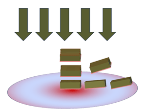
The chiplet evolution
Large chipmakers have been constrained by the size of the reticle field for at least the last several process nodes, which sharply limited the number of features that could be crammed onto a planar SoC. Today, with node shrinks becoming more costly and challenging, the best solution available is to decompose the SoC into individual blocks, or chiplets.

“Once the dies become really big, you’re up against the reticle limit,” says Intel’s Das Sharma. “That’s where you will see a lot of people deploying chiplets. You’re basically having multiple sets of chips being packaged together to deliver a certain set of functionality.”

Take, for instance, the leap to 50 Tb per second switches that are challenging the limits of reticle size. There’s a growing need to dissect and distribute the functionality of these chips across multiple components. Whether it’s the I/O, memory, or SRAM, the key lies in strategically breaking down the SoC into smaller units. This not only makes the manufacturing process more feasible, but also opens doors to more innovative and efficient design architectures.

It also provides some immediate benefits. Smaller dies yield better than larger ones, which is why in 2012 Xilinx split its 28nm FPGA into four different dies, connected through an interposer. It also provides room to grow, because the individual chiplets are still well below the reticle limit.

But all of the early implementations were homogeneous. They were all developed by the same vendor using the same process technology. A big benefit of advanced packaging is the ability to combine heterogeneous chiplets in the same package, allowing analog circuits and less-critical features to be developed at whatever process node makes sense. This is the challenge facing large chipmakers, foundries, and OSATs today, and it’s one that has not yet been fully solved.

Nevertheless, the chip industry agrees on one thing. There needs to be a common way to connect all of these chiplets together, and this is where UCIe fits into the picture.

The UCIe standard
Achieving a consensus on the electrical characteristics that underpin the UCIe is akin to orchestrating a symphony with a multitude of instruments, each with its own acoustic signature. Ensuring that chiplets from different corners of the industry can connect and communicate efficiently necessitates bridging gaps in voltage levels, signal timing, and power distribution.

In March, 2022, the UCIe consortium released UCIe 1.0 that included specifications for a standardized physical die-to-die interface designed to facilitate seamless communication between chiplets, regardless where they were manufactured or by whom. The specifications encompassed key aspects, such as electrical properties, physical dimensions, and protocols necessary for ensuring compatibility and efficient data transfer between diverse chip components.

“On advanced packages at 45 microns, the numbers are pretty stellar,” says Das Sharma. “You have 188 gigabytes per second per square millimeter as a starting point, up to 1.35 terabytes per second per square millimeter. People will have a hard time even absorbing that kind of bandwidth and processing it.”

UCIe 1.0 uses a layered protocol approach. The physical layer underpins the protocol stack, dedicated to defining and managing electrical signaling, such as clock synchronization and link training, while also incorporating sideband communication channels essential for non-data interactions between chiplets.

At the heart of UCIe’s mechanics is the Die-to-Die (D2D) adapter. This crucial interface acts as the gatekeeper, managing link state and facilitating negotiation parameters for chiplets, crucial for establishing reliable chiplet communication. It optionally extends a safeguard for data integrity through mechanisms like cyclic redundancy check (CRC) and link-level retry capabilities. This not only ensures accuracy in high-speed data transfer, but also aligns different chiplet protocols by providing an arbitration system enabling multiple chips to interact efficiently.

“UCIe is pretty flexible in that way,” says Chaudhry. “It supports your PCIe protocols, XML protocol, or streaming, so you can decide which protocol you want to support. And it has different data rates that it supports. It’s the lowest common denominator that everybody will support. If you’re on a 3nm process, you can support a much higher data rate, but if the other chiplet is at a different process node, then both the parts will support the basic lowest common denominator of the spec, and then you can talk on that.”

UCIe also incorporates strategies to mitigate interconnect defects, such as stuck-at faults and signal discontinuities. Stipulations within UCIe include the implementation of auxiliary pathways, furnishing a means to maintain connectivity if the primary lanes fail. This redundancy helps sustain system functionality by providing avenues for fault tolerance and repair.

UCIe also embraces existing standards such as PCI Express (PCIe) and Compute Express Link (CXL) natively, ensuring a broad resonance across the industry by capitalizing on these well-established protocols. The layered approach of UCIe also encompasses comprehensive usage models.

In August 2023, the consortium published UCIe version 1.1, extending reliability mechanisms to more protocols and supporting additional usage models. These enhancements are not merely incremental. They are geared towards pivotal segments such as automotive, which is gravitating toward chiplets.

One key area where the evolution from UCIe 1.0 to 1.1 becomes evident is in the standard’s preventive monitoring features. UCIe 1.1 expands the protocol with new registers designed to capture detailed Eye Margin information — viewing both width and height — which provides standardized reporting formats and proactive link health monitoring. Rather than reinventing the wheel, UCIe 1.1 leverages the existing periodic parity Flit injection mechanism from version 1.0, enhancing error detection and reporting capabilities through a new error log register. That, in turn, allows for improved assessment of link repair necessities. UCIe 1.1 also offers enhancements for compliance testing.

Another notable aspect is the advent of new and emerging usages, particularly with streaming protocols. Whereas UCIe 1.0’s support for such protocols was restricted to Raw Mode, UCIe 1.1 extends the utility of the die-to-die (D2D) adapter on the FDI interface to streaming protocols. This extension enables a blend of CRC retry power management features and facilitates the coexistence of multiple protocols.

UCIe 1.1 also considers cost optimization for advanced packaging solutions in anticipation of shrinking bump pitches and the advent of 3D integration. The introduction of additional column arrangements in UCIe 1.1 creates broader opportunities for mix-and-match dies.

“In a chiplet environment, the dies are very close to each other and your shoreline is very limited,” says Chaudhry. “You have limited space to connect the dies, and how the number of pins are connected, facing each other, that becomes critical. That is one thing that UCIe is addressing. What should be the pin location? Whether it’s 6-, 8-, or 16-column, how do you arrange it so that when one vendor has an 8-column configuration, they can talk to one with a 12 column configuration and connect to it physically, not just in terms of pins, but also connectivity and shoreline compatibility?”

Designing for interoperability
There are a number of technical hurdles that still stand in the way of the widespread adoption of UCIe. These include a need for precise electrical conformity, predictable signaling realms, and systematic physical interconnects catering to a variety of nodes and manufacturing processes.

“You can also have HBM in there, which can be very tall compared to a single ASIC,” says Amkor’s Chaudhry. “How do you address those height differences? A lot of different issues come into play when you’re putting different dies and different chiplets together.”

Thermal management is also a key element for high-density packaging. Disparate process nodes inevitably present distinct power profiles and heat dissipation characteristics. Bridging these gaps necessitates innovative heat distribution methodologies and sophisticate warpage control to ensure structural integrity and reliable function in complex modules.

“There are a lot of challenges in thermal,” adds Chaudhry. “When you have two dies from different process nodes, how do you make sure that you have a way to dissipate the power equally? Those are some of the challenges as we go along and there’s no general solution to that yet. Those are kind of things that the consortium is looking at right now.”

Continued evolution
Another goal of the UCIe consortium is to ensure that anyone developing a chiplet today will still be able to use that design five years from now, despite progress in the standard during that time.

“It will absolutely evolve,” adds Chaudhry. “PCI did the same thing. They are on Gen 5 or Gen 6 now. USB is the same way with USB 4.0 coming soon. CXL is at 3.1. We expect the same thing to happen to UCIe. It will continuously improve and come up with new and more flexible solutions that our members can adopt.”

“The more people get involved, the more they’re going to start tweaking things,” adds Das Sharma. “Some of them are not going to work out, and some of them are going to work out really well. This is a multi-decade journey, and the key is to learn and adapt and keep moving on.”

Conclusion
The UCIe initiative aims to revolutionize chip package interconnectivity by emulating the success of Peripheral Component Interconnect Express (PCIe) at the PCB level. By facilitating direct inter-die connections within the chip package, UCIe endeavors to drastically cut power usage, enhance bandwidth efficiency, and, ultimately, reduce production costs.

“The good thing about UCIe is that it’s an open standard,” says Chaudhry. “In all, there are about 120 members, and all of them are working together. There are six different working groups that range from mechanical to electrical to security to software and marketing, where they are bringing up new things as they are developing their chiplet-based designs. A lot of things that have happened between UCIe 1.0 and 1.1 are basically due to their input.”

—Ed Sperling contributed to this report.

The post UCIe Goes Back To The Drawing Board appeared first on Semiconductor Engineering.

  • ✇Semiconductor Engineering
  • Building CFETs With Monolithic And Sequential 3DKatherine Derbyshire
    Successive versions of vertical transistors are emerging as the likely successor to finFETs, combining lower leakage with significant area reduction. A stacked nanosheet transistor, introduced at N3, uses multiple channel layers to maintain the overall channel length and necessary drive current while continuing to reduce the standard cell footprint. The follow-on technology, the CFET, pushes further up the z axis, stacking n-channel and p-channel transistors on top of each other, rather than sid
     

Building CFETs With Monolithic And Sequential 3D

Successive versions of vertical transistors are emerging as the likely successor to finFETs, combining lower leakage with significant area reduction.

A stacked nanosheet transistor, introduced at N3, uses multiple channel layers to maintain the overall channel length and necessary drive current while continuing to reduce the standard cell footprint. The follow-on technology, the CFET, pushes further up the z axis, stacking n-channel and p-channel transistors on top of each other, rather than side by side.

In work presented at December’s IEEE Electron Device Meeting, researchers at TSMC estimated that CFETs give a 1.5X to 2X overall size reduction at constant gate dimensions. [1] Those are significant area benefits for any digital logic, but manufacturing these new transistor structures will be a challenge.

Monolithic 3D integration is the simplest integration scheme, and the one likely to see production first. In monolithic 3D integration, the entire structure is assembled on a single piece of silicon. This approach can also be used to fabricate compute-in-memory designs where memory devices are fabricated as part of the metallization layers for a conventional CMOS circuit. While individual layers in monolithic 3D designs can incorporate new technologies — the integration of ReRAM devices, for example — the overall CMOS flow is preserved. All of the materials and processes used must be compatible with that rubric.

Adding more nanosheets for complementary devices
The overall process in this kind of scheme is similar to a stacked nanosheet transistor flow. It starts with a stack of eight or more alternating silicon and silicon germanium layers (four pairs), compared to a stacked nanosheet NFET or PFET, which might have only four such layers (two pairs). In a CFET flow, however, middle dielectric layer is inserted halfway through the stack.

This layer, separating the n-type and p-type transistors, is probably the most important difference from a standard nanosheet transistor flow. To minimize parasitic capacitance, the middle dielectric layer should be as thin as possible, said imec’s Naoto Horiguchi. If it’s too thin, though, edge placement errors can cause isolation failures, landing contacts for the top devices onto bottom devices. [2]

In TSMC’s process, the Si/SiGe superlattice includes a high-germanium SiGe layer as a placeholder for the middle dielectric. After the source/drain etch, a highly selective etch removes this layer and oxidizes the silicon on either side of it to form the middle dielectric.

The inner spacer recess etch, which follows middle dielectric formation in the TSMC process, indents the SiGe layers relative to the silicon nanosheets, defining the gate length and junction overlap.

While TSMC emphasized it has not yet made fully metallized integrated CFET circuits, it did report that more than 90% of the transistors survived.

Fig. 1: TSMC used monolithic integration to stack NFET and PFET devices. [1]

Depositing the nanosheet stack is straightforward. Etching it with the precision required is not. A less-than-vertical etch profile will change the relative channel lengths of the top and bottom devices, leading to asymmetric switching characteristics.

Stacking wafers for more flexibility
The alternative, sequential 3D integration is a bit more flexible. While monolithic 3D integration uses a single device layer, sequential 3D integration bonds an additional tier on top of the first. Sequential 3D integration is different from three-dimensional wafer-level packaging and chip stacking, though. In WLP, the component devices are finished, passivated, and tested. The component chips are fully functional as independent circuits. In sequential 3D integration, the two tiers are part of a single integrated circuit.

Often, though not always, the second tier is an unprocessed bare wafer with no devices at all. Ionut Radu, director of research and external collaborations at Soitec, said his company used its SmartCut process to transfer sub-micron silicon layers. [3] One of the advantages of sequential integration, though, is that it opens the door to other possibilities. For example, the second layer could use a different silicon lattice orientation to facilitate stress engineering for improved carrier mobility. It also could use an alternative channel material, such as GaAs or a two-dimensional semiconductor. And up until the transfer occurs, processing of the second wafer has no effect on the thermal budget of the first.

After bonding, the second tier’s process temperature generally must remain below 500° C. Tadeu Mota-Frutuoso, process integration engineer at CEA-Leti, said researchers were able to achieve this benchmark in a conventional CMOS process by using laser annealing for the source/drain activation steps. [4]

While sequential 3D integration can be used to realize CFET devices, the top layers also can contain independent circuitry. Still, as in monolithic integration, the dielectric layer between the two circuit tiers is a critical process step. Analysts at KAIST found that reducing the thickness of the interlayer dielectric improves heat dissipation. It also facilitates the use of a bottom gate to control the top tier devices. On the other hand, the dielectric layer lies at the interface between the original wafer and the transferred layer. Thickness control depends on the polishing step used to prepare the transfer surface. Such precise control is extremely challenging for CMP. [5]

Re-driving wafers without contamination
While the second circuit tier can be added at any point in the process flow, the insertion point constrains not only the first and second tier devices, but also the fab as a whole. When the second layer does not yet contain devices, alignment to the first layer is relatively easy. In contrast, Horiguchi said, aligning one device wafer on top of another imposes an area penalty to accommodate potential overlay error. The total device thickness of sequential 3D structures tends to be greater, as well.

Returning a first-tier wafer with contacts and other metallization to FEOL tools for fabrication of a second transistor layer poses a substantial cross contamination risk. Even if the top surface is well encapsulated, Mota-Frutuoso explained in an interview that the sidewalls and bevels of the bottom tier can still expose metal layers to FEOL processes. CEA-Leti’s proposed bevel contamination wrap (BCW) scheme first cleans the wafer edge, then encapsulates it and the sidewall in a protective oxide layer.

"Fig.

Fig. 2: CEA-Leti’s sequential 3D integration stacked silicon CMOS on an industrial 28nm FDSOI wafer. [4]

Controlling heat dissipation
Heat dissipation is a major challenge for both monolithic and sequential 3D devices. Generalizations are difficult because thermal characteristics depend on the specific integration scheme and even the circuit design. Wei-Yen Woon, senior manager at TSMC, and his colleagues evaluated AlN and diamond as possible thermal dissipation layers. While both have been used in power devices, they are new to CMOS process flows. They achieved good quality columnar AlN films with a low temperature sputtering process, though the columnar structure did impede in-plane heat transport. While diamond offers extremely high thermal conductivity, it also can require extremely high process temperatures. The TSMC group deposited thin films with acceptable quality at BEOL compatible temperatures by using pre-deposited diamond nuclei, but they have not yet attempted to integrate these films with working devices.[6]

What’s next?
In the short term, monolithic 3D integration offers a relatively straightforward path to CFET fabrication, building on existing nanosheet transistor process flows. Even proponents of sequential 3D integration expect the monolithic approach to reach production first. For the longer term, though, the ability to use a completely different material for the second device layer gives device designers many more process optimization knobs.

However it is achieved, the idea that active devices no longer need to confine themselves to a single planar layer has implications far beyond logic transistors. From compute-in-memory modules to image sensors, 3D integration is an important tool for “More than Moore” devices.

References

[1] S. Liao et al., “Complementary Field-Effect Transistor (CFET) Demonstration at 48nm Gate Pitch for Future Logic Technology Scaling,” 2023 International Electron Devices Meeting (IEDM), San Francisco, CA, USA, 2023, pp. 1-4, doi: 10.1109/IEDM45741.2023.10413672.

[2] N. Horiguchi et al., “3D Stacked Devices and MOL Innovations for Post-Nanosheet CMOS Scaling,” 2023 International Electron Devices Meeting (IEDM), San Francisco, CA, USA, 2023, pp. 1-4, doi: 10.1109/IEDM45741.2023.10413701.

[3] I. Radu et al., “Ultimate Layer Stacking Technology for High Density Sequential 3D Integration,” 2023 International Electron Devices Meeting (IEDM), San Francisco, CA, USA, 2023, pp. 1-4, doi: 10.1109/IEDM45741.2023.10413807.

[4] T. Mota-Frutuoso et al., “3D sequential integration with Si CMOS stacked on 28nm industrial FDSOI with Cu-ULK iBEOL featuring RO and HDR pixel,” 2023 International Electron Devices Meeting (IEDM), San Francisco, CA, USA, 2023, pp. 1-4, doi: 10.1109/IEDM45741.2023.10413864.

[5] S. K. Kim et al., “Role of Inter-Layer Dielectric on the Electrical and Heat Dissipation Characteristics in the Heterogeneous 3D Sequential CFETs with Ge p-FETs on Si n-FETs,” 2023 International Electron Devices Meeting (IEDM), San Francisco, CA, USA, 2023, pp. 1-4, doi: 10.1109/IEDM45741.2023.10413845.

[6] W. Y. Woon et al., “Thermal dissipation in stacked devices,” 2023 International Electron Devices Meeting (IEDM), San Francisco, CA, USA, 2023, pp. 1-4, doi: 10.1109/IEDM45741.2023.10413721.


The post Building CFETs With Monolithic And Sequential 3D appeared first on Semiconductor Engineering.

Techniques To Identify And Correct Asymmetric Wafer Map Defects Caused By Design And Process Errors

Od: James Kim
22. Únor 2024 v 09:03

Asymmetries in wafer map defects are usually treated as random production hardware defects. For example, asymmetric wafer defects can be caused by particles inadvertently deposited on a wafer during any number of process steps. In this article, I want to share a different mechanism that can cause wafer defects. Namely, that these defects can be structural defects that are caused by a biased deposition or etch process.

It can be difficult for a process engineer to determine the cause of downstream structural defects located at a specific wafer radius, particularly if these defects are located in varying directions or at different locations on the wafer. As a wafer structure is formed, process behavior at that location may vary from other wafer locations based upon the radial direction and specific wafer location. Slight differences in processes at different wafer locations can be exaggerated by the accumulation of other process steps as you move toward that location. In addition, process performance differences (such as variation in equipment performance) can also cause on-wafer structural variability.

In this study, structural defects will be virtually introduced on a wafer to provide an example of how structural defects can be created by differences in wafer location. We will then use our virtual process model to identify an example of a mechanism that can cause these types of asymmetric wafer map defects.

Methods

A 3D process model of a specific metal stack (Cu/TaN/Ta) on a warped wafer was created using SEMulator3D virtual fabrication (figure 1). After the 3D model was generated, electrical analysis of 49 sites on the wafer was completed.

In our model, an anisotropic barrier/liner (TaN/Ta) deposition process was used. Due to wafer tilting, there were TaN/Ta deposition differences seen across the simulated high aspect ratio metal stack. To minimize the number of variables in the model, Cu deposition was assumed to fill in an ideal manner (without voids). Forty-nine (49) corresponding 3D models were created at different locations on the wafer, to reflect differences in tilting due to wafer warping. Next, electrical simulation was completed on these 3D models to monitor metal line resistance at each location. Serpentine metal line patterns were built into the model, to help simulate the projected electrical performance on the warped wafer at different points on the same radius, and across different directions on the wafer (figure 2).

Illustration of an anisotropic liner/barrier metal deposition on a tilted silicon wafer structure caused by wafer warping. In the illustration, the deposition direction is represented by arrows at the top of the image pointed down toward a silicon wafer at the bottom of the image. Forty-nine (49) corresponding 3D models were created at different locations on the wafer, to reflect differences in tilting due to wafer warping. These 49 models are represented in the image by rectangular blocks shown between the deposition direction arrows and the silicon wafer itself.

Fig. 1: Anisotropic liner/barrier metal deposition on a tilted structure caused by wafer warping.

Composite image displaying the resistance extraction simulation and cross section analysis performed in this study. 4 images make up the composite image. Upper left: 3D visualization of serpentine metal line patterns built into the model. Upper right: Top view of TaN/Ta deposition in simulated high aspect ratio metal stack, along with visible Cu deposition (shown in brown and blue colors). Lower left: Cross section view of metal stack. Lower right: Resistance extraction simulation of serpentine metal line patterns, with different colors (blue to red) highlighting areas of lower to higher resistance.

Fig. 2: Resistance extraction simulation and cross section analysis.

Using only incoming structure and process behavior, we can develop a behavioral process model and extend our device performance predictions and behavioral trend analysis outside of our proposed process window range. In the case of complicated processes with more than one mechanism or behavior, we can split processes into several steps and develop models for each individual process step. There will be phenomena or behavior in manufacturing which can’t be fully captured by this type of process modeling, but these models provide useful insight during process window development.

Results

Of the forty-nine 3D models, the models on the far edge of the wafer were heavily tilted by wafer warpage. Interestingly, not all of the models at the same wafer radius exhibited the same behavior. This was due to the metal pattern design. With anisotropic deposition into high aspect ratio trenches, deposition in specific directions was blocked at certain locations in the trenches (depending upon trench depth and tilt angle). This affected both the device structure and electrical behavior at different locations on the wafer.

Since the metal lines were extending across the x-axis, there were minimal differences seen when tilting the wafer across the x-axis in our model. X-axis tilting created only a small difference in thickness of the Ta/TaN relative to the Cu. However, when the wafer was tilted in the y-axis using our model, the high aspect ratio wall blocked Ta/TaN deposition due to the deposition angle. This lowered the volume of Ta/TaN deposition relative to Cu, which decreased the metal resistance and placed the resistance outside of our design specification.

X-axis wafer tilting had little influence on the device structure. The resistance on the far edge of the x-axis did not significantly change and remained in-spec. Y-axis wafer tilting had a more significant influence on the device structure. The resistance on the far edge of the y-axis was outside of our electrical specification (figure 3).

Electrical simulation results shown on a wafer map. Locations on the far edge of the Y-axis exhibit out-of-spec resistance. Resistance varied between 40,430 and 40,438 ohm/SQ across the wafer. In the image, out of spec resistance on the wafer is highlighted in blue (lower resistance within the range) or red (higher resistance within the range).

Fig. 3: Electrical simulation results shown on a wafer map. Locations on the far edge of the Y-axis exhibit out-of-spec resistance.

Conclusion

Even though wafer warpage occurs in a circular manner due to accumulated stress, unexpected structural failures can occur in different radial directions on the wafer due to variations in pattern design and process behavior across the wafer. From this study, we demonstrated that asymmetric structures caused by wafer warping can create top-bottom or left-right wafer performance differences, even though processes have been uniformly applied in a circular distribution across the wafer. Process simulation can be used to better understand structural failures that can cause performance variability at different wafer locations. A better understanding of these structural failure mechanisms can help engineers improve overall wafer yield, by taking corrective action (such as performing line scanning at specific wafer locations) or by adjusting specific process windows to minimize asymmetric wafer defects.

The post Techniques To Identify And Correct Asymmetric Wafer Map Defects Caused By Design And Process Errors appeared first on Semiconductor Engineering.

  • ✇Semiconductor Engineering
  • Utilizing Artificial Intelligence For Efficient Semiconductor ManufacturingVivek Jain
    The challenges before semiconductor fabs are expansive and evolving. As the size of chips shrinks from nanometers to eventually angstroms, the complexity of the manufacturing process increases in response. It can take hundreds of process steps and more than a month to process a single wafer. It can subsequently take more than another month to go through the assembly, testing, and packaging steps necessary to get to the final product. Artificial Intelligence (AI) can be deployed within a fab to a
     

Utilizing Artificial Intelligence For Efficient Semiconductor Manufacturing

22. Únor 2024 v 09:02

The challenges before semiconductor fabs are expansive and evolving. As the size of chips shrinks from nanometers to eventually angstroms, the complexity of the manufacturing process increases in response. It can take hundreds of process steps and more than a month to process a single wafer. It can subsequently take more than another month to go through the assembly, testing, and packaging steps necessary to get to the final product.

Artificial Intelligence (AI) can be deployed within a fab to address the complexity and intricacy of semiconductor manufacturing. A fab generates petabytes of data as wafers go through the multitude of process and test operations. This wealth of data also presents a challenge in that it needs to be analyzed and acted on quickly to ensure tight process control, high yield, and avoid process excursions. Beyond navigating the complexity of the manufacturing process, new solutions are necessary to help make the process as efficient as possible and the yield as high as possible to produce the most business value for fabs.

The benefits of AI-enabled analysis tools for IC manufacturers

Traditional techniques to detect issues in the manufacturing process have run out of steam, especially at advanced technology nodes. For example, an engineer must do their own yield analysis to seek out potential problems. Once they identify an issue, they communicate with the defect and process teams to determine the root cause and then troubleshoot it. The defect team will begin work to find some correlation behind the issue and the process team troubleshoot and link it to the root cause.

All these steps take up significant time that could be focused on achieving the highest yield of chips possible, driving costs down and reducing time to market. One of the biggest benefits of enabling AI in analysis tools is that an engineer can quickly recognize and pinpoint an issue in a specific chip to see which process step and/or equipment has caused the issue.

Beyond the fast and accurate process control that AI allows for, there are numerous other benefits that result from the saved time and money, including:

  • Predictive applications: Enables fabs to take leap from reactive to predictive process control
  • Scalability: Analyzes petabytes of data, connects multiple fabs, and comes cloud-ready
  • Efficiency: Allows fab to make better decisions and reduce false alarms

To enable the next generation of manufacturing, Synopsys is enabling AI and Machine Learning (ML) for a comprehensive process control solution.

Actionable insights with AI and ML

Wafer, equipment, design, mask, test, and yield are silos within a fab that can benefit from a comprehensive AI/ML enabled solution. Such a solution can specifically help engineers generate actionable insights into the following:

  • Fault detection and classification (FDC)
  • Statistical process control (SPC)
  • Dynamic fault detection (DFD)
  • Defect classification and image analytics
  • Defect image analytics
  • Decision support system (DSS)

Fast analysis of petabytes of data, from equipment sensors or process parameters, allows manufacturers to quickly identify the root cause of process excursions and take action to maintain yield.

AI and ML in the fab

Synopsys is a provider of software solutions for silicon manufacturing and silicon lifecycle management, including solutions for TCAD, mask solutions, and manufacturing analytics. Its existing solutions are connected to thousands of pieces of equipment over multiple fabs with millions of sensors, analyzing hundreds of petabytes of data. By providing real-time visibility into the manufacturing process, Synopsys enables predictive analytics and optimizes product quality and yield to help give semiconductor fabs a leg up in this competitive landscape.

Synopsys has introduced an AI/ML enabled software offering, Fab.da, to make semiconductor manufacturing efficient. Fab.da is a part of the Synopsys EDA Data Analytics solution, which brings together data analytics and insights from the entire chip lifecycle

It offers a complete data continuum by bringing together these different data types from many different sources into one platform for both advanced and mature node chips. This data continuum allows for high user productivity, maximum data scalability, and increased speed and accuracy in root cause analysis for issues.

Delivering process control solutions to manage complexity at leading-edge fabs, Fab.da can help chip designers and manufacturers drive operational excellence and productivity, providing a competitive edge in today’s manufacturing landscape.

The post Utilizing Artificial Intelligence For Efficient Semiconductor Manufacturing appeared first on Semiconductor Engineering.

  • ✇Semiconductor Engineering
  • Integrating Digital Twins In Semiconductor OperationsMark da Silva
    By Mark da Silva, Nishita Rao and Karim Somani Chipmakers must adopt transformative technologies including Digital Twins (DT) to keep pace with unprecedented global semiconductor industry growth that is expected to drive its total market value to $1 trillion[1] as soon as 2030. Leveraging predictive modeling and other efficiency-enhancing innovations, DTs promise to optimize semiconductor design, manufacturing processes and equipment maintenance while improving overall operational efficiency. Wi
     

Integrating Digital Twins In Semiconductor Operations

22. Únor 2024 v 09:01

By Mark da Silva, Nishita Rao and Karim Somani

Chipmakers must adopt transformative technologies including Digital Twins (DT) to keep pace with unprecedented global semiconductor industry growth that is expected to drive its total market value to $1 trillion[1] as soon as 2030. Leveraging predictive modeling and other efficiency-enhancing innovations, DTs promise to optimize semiconductor design, manufacturing processes and equipment maintenance while improving overall operational efficiency.

With DTs rising in prominence as a critical enabler of industry growth, key players from across the semiconductor ecosystem – including OEMs, platforms and end users – gathered at the Semiconductor Digital Twin Workshop last December at SEMI headquarters in Milpitas, Calif. to discuss the latest DT developments and explore the path to advancing the technology.

Following are highlights from the sold-out event hosted by the SEMI Smart Manufacturing Initiative.

Key takeaways

  • Industry Alignment on DT Definition and Taxonomy
    • The semiconductor industry needs to align on the definition and taxonomy of DTs in semiconductor operations.
    • With collaboration crucial to advances in DTs, the industry must come together to develop a common understanding of the technology.
  • Data Sharing for Sustainability Improvements
    • Sharing data among various chip ecosystem players will be vital to driving sustainability improvements.
    • Focusing on equipment and operational DTs with sustainability in mind will help foster collaboration among industry stakeholders.
  • Advocacy for Standardized DT Architecture and Framework
    • A standardized DT framework architecture must be established to enhance interoperability, reliability, synchronization, and security.
    • The adoption of digital twin technical standards is in its early stages but increasing in importance as DT technology evolves.
    • Collaboration will be essential to accelerate the availability and adoption of several digital twin technical standards under development by SEMI and other Standards Development Organizations (SDOs).

Key challenges

  • Robust DT Framework and Overcoming Development Silos
    • Establishing a robust DT framework and overcoming isolated development silos in microelectronics are challenges the industry must overcome.
  • Managing Unclean Factory Data
    • Challenges include managing unclean factory data, varying data granularity, and addressing the lifecycle of data models.
  • Sharing Data Between Tools and Process Steps
    • Data sharing between various semiconductor tools and process steps must be seamless. Data provenance is critical for DT accuracy and validation.
  • Legacy Factories & Small/Medium Firms
    • Factories with older generation tools and processes have a unique challenge in developing process level DTs for existing products.

Workshop sessions

The workshop consisted of four sessions focused on DT efforts by equipment makers, solution providers, device makers, and factory integration providers.

Equipment-level digital twins session

The session focused on OEM efforts to develop tool-level DTs and highlighted the potential to improve efficiency, performance, and sustainability. The session also featured discussions on equipment-level data sharing, standards, and interoperability challenges that need to be addressed. Speakers included IRDS Co-Chair Supika Mashiro of TEL, Ala Moradian of Applied Materials, Joseph Ervin of LAM Research, Sean Glazier of Onto Innovation, Basil Milton and Chan-Pin Chong of Kulicke & Soffa, and Mark Huntington of McKinsey & Company.

Session speakers: (L) Supika Mashiro, TEL, and (R) Ala Moradien, AMAT. 

Speakers discussed existing DTs deployed in manufacturing such as Run-to-Run (R2R) control, virtual metrology, and predictive maintenance (PdM) and the need for standardized DTs that can communicate with each other. Tool-level DT solutions such as Applied Materials EcoTwin within the AppliedTwin platform provide a virtualized replica of chipmaking equipment for development and improvement of chip-level processes. The platform has also demonstrated extensibility to sustainability analysis, a significant development.

Other focus areas were the connectivity of DTs across different levels (tools to factories) and the use of AI to make them self-adjusting for manufacturing processes. The importance of DT infrastructure and associated challenges such as ensuring clean and accessible data, data flow, and communication to keeping DTs synchronized were raised as significant challenges. In the back-end, OEMs are making steady progress to virtualize various tools such as wire bonding. The session also highlighted DTs as a major investment across industries, with huge potential in chipmaking. Building a strong data sharing foundation is key to success.

Chamber process, operations and planning level digital twin session

The session was led by solution providers from across the semiconductor ecosystem that develop tools to facilitate DTs at various hierarchical levels. The providers offer a variety of products and services across areas such as process physics-based models, chamber processes, operations, as well as planning modelling approaches to help companies implement and manage DTs. The session included technical details of DT models and their potential impact on the entire manufacturing process.

While the session made clear that DTs promise to revolutionize the semiconductor industry, it must overcome significant technical development challenges of integrating DTs into day-to-day operations. Speakers included Sarbajit Ghosal of SC Solutions, Norman Chang of Ansys, Holland Smith of INFICON, Chandra Reddy of IBM Research, Jon Herlocker of TIGNIS, Ken Smerz of ZELUS and John Behnke of INFICON.

Speakers emphasized the need for fast, multi-physics-based (and data-assisted) accurate DTs for real-time control and monitoring and that react instantly to changes, just like physical equipment. Think of it as having a virtual process line that can predict how different processes will interact. Sitting on top of the DTs are AI-powered (physics and/or data-driven) models that can then be harnessed to optimize manufacturing processes and predict yield.

Speakers also discussed operational-level DTs and the need for a central hub for all factory operational data to boost efficiency, maximize productivity, and reduce waste – all critical as the number of fabs grows in the years ahead. Construction DTs for pre-construction planning in the building of new chip fabs or expanding brown-field sites provide a preconstruction virtual blueprint that can help identify potential problems early on and minimize time to wafer starts. Lastly, how these various levels of DTs are integrated vertically within a factory play a key role in making decisions about autonomous fabs.

Digital twin adoption and implementation session

The session was led by device makers and owners of fabs, where DTs are critical for improving productivity by predicting yield, quality, and efficiency. A process-level DT enables a virtual representation of a product’s process flow in the fab, and it can be used to speed integration efforts (MRL 5-7), simulate specific outcomes, and optimize operations. Imagine a future where chip fabs are run by AI agents, with virtual models predicting problems before they happen and optimizing processes on the fly. That’s the vision shared by the session’s expert speakers. Their insights painted a fascinating picture of what’s next for the semiconductor industry. Speakers included Professor. H.-S Philip Wong of Stanford University, Steven J Meyer of Intel, Jae Yong Park of Samsung, Rosa Javadi of JABIL, Professor Amit Lal and Peter Doerschuk of Cornell University, Ben Davaji of Northeastern University, Pushkar Apte of SEMI and Bobby Mitra of Deloitte.

Session speakers: (L) Steven J Meyer, Intel, and (R) Jae Yong Park, Samsung.

The key development target is advanced AI-assisted manufacturing with three layers of virtual models – processes, tools, and the entire fab itself – all working together seamlessly is critical. This ambitious vision aligns with the National Semiconductor Technology Center (NSTC) DT Grand Challenge, which focuses on generating, sharing, and using data effectively. Intel’s AFS Software Suite, which includes high-speed simulators and graphical models to enable better planning and decision-making across multiple sites, is a real-world example of DTs used in today’s fabs.

Use cases of deploying AI to improve Automated Material Handling Systems (AMHS) asset utilization by 30% have also been demonstrated in real-world fab environments. The session highlighted the importance of scheduling with AI-powered DTs and standardizing data availability across the industry. Other impressive product development use case studies shared included a rapid COVID-19 tester system development and a global supply chain DT.

Speakers described how challenges such as infrastructure readiness, talent gaps, and data privacy concerns are slowing industrywide adoption. They also discussed efforts to develop an open-access academic cleanroom dedicated to developing and testing DT models for lithography and etching processes, with investigation of federated learning to address data privacy & sharing concerns. The experts characterized the hierarchy of DT types as a framework based on the ISA-95 standard to ensure seamless communication and collaboration between DTs across various levels, from process development to production. This interconnected approach could revolutionize chipmaking across the entire enterprise, as demonstrated by an example showing DTs spanning the enterprise.

Digital twin connectivity and platform integration session

The session focused on a variety of product and service offerings by cloud, facilities, and supply chain solution providers that help companies implement and manage DTs of various levels. These solutions include integration, connectivity, security and horizontal integration across the supply chain. Almost all speakers pointed to the importance of standardization efforts as crucial for future development. Speakers included Rad Desiraju of Microsoft, Gautham Unni of AWS, David Gross and Srividya Jayaram of Siemens, Slava Libman of FTD Solutions, Becky Kelderman of Rockwell Automation, Ram Walvekar of HCL Technologies, and Paul Trio of SEMI International Standards

Session speakers touched on definitions and categorization of DTs, including types and uses, as well as building dedicated infrastructure to support their development. The experts highlighted a few DT development challenges in areas such as data sources and provenance, as well as visualization and shared their solution offerings for creating, connecting, and maintaining these digital twins both vertically and horizontally within an enterprise.

The presenters also shared use cases on how DTs bridge design and manufacturing, enabling simulations and faster production, and how connecting DTs for various assets, processes, and products creates a holistic view. Session speakers also discussed a DT maturity scorecard that enables players from across the supply chain to track their progress and identify areas for improvement. Use cases of facility-level DTs for water management in fabs for promoting sustainability was also a topic of discussion.

The semiconductor industry’s commitment to digital twins

The Semiconductor Digital Twin Workshop showcased the industry’s commitment to adopting and advancing the technology. Continued collaboration and adherence to standards and sustainable practices will play a crucial role in unlocking the full potential of DT technology in semiconductor manufacturing.

SEMI thanks the speakers who provided access to their material presented at the workshop. Visit Semiconductor Digital Twin Workshop OnDemand | SEMI for the workshop materials.

Reference

  1. Ondrej Burkacky, Julia Dragon, and Nikolaus Lehmann, The semiconductor decade: A trillion-dollar industry, McKinsey & Company (blog), April 1, 2021

Nishita Rao is senior product marketing manager at SEMI.

Karim Somani is program manager at SEMI.  

The post Integrating Digital Twins In Semiconductor Operations appeared first on Semiconductor Engineering.

Make The Impossible Possible: Use Variable-Shaped Beam Mask Writers And Curvilinear Full-Chip Inverse Lithography Technology For 193i Contacts/Vias With Mask-Wafer Co-Optimization

22. Únor 2024 v 09:01

Abstract:

“Full-chip curvilinear inverse lithography technology (ILT) requires mask writers to write full reticle curvilinear mask patterns in a reasonable write time. We jointly study and present the benefits of a full-chip, curvilinear, stitchless ILT with mask-wafer co-optimization (MWCO) for variable-shaped beam (VSB) mask writers and validate its benefits on mask and wafer at Micron Technology. The full-chip ILT technology employed, first demonstrated in a paper presented at the 2019 SPIE Photomask Technology Conference, produces curvilinear ILT mask patterns without stitching errors, and with process windows enlarged by over 100% compared to the OPC process of record, while the mask was written by multibeam mask writer. At the 2020 SPIE Advanced Lithography Conference, a method was introduced in which MWCO is performed during ILT optimization. This approach enables curvilinear ILT for 193i masks to be written on VSB mask writers within a practical, 12-h time frame, while also producing the largest process windows. We first review MWCO technology, then curvilinear ILT mask patterns written by VSB mask writer, and then show the corresponding 193i process wafer prints. Evaluations of mask write times and mask quality in terms of critical dimension uniformity and process windows are also presented.”

Find the technical paper here. Published February 2024.

Pang, Linyong, Sha Lu, Ezequiel Vidal Russell, Yang Lu, Michael Lee, Jennefir Digaum, Ming-Chuan Yang et al. “Make the impossible possible: use variable-shaped beam mask writers and curvilinear full-chip inverse lithography technology for 193i contacts/vias with mask-wafer co-optimization.” Journal of Micro/Nanopatterning, Materials, and Metrology 23, no. 1 (2024): 011207-011207.

Author Affiliations: D2S Inc. and Micron Technology Inc.

The post Make The Impossible Possible: Use Variable-Shaped Beam Mask Writers And Curvilinear Full-Chip Inverse Lithography Technology For 193i Contacts/Vias With Mask-Wafer Co-Optimization appeared first on Semiconductor Engineering.

  • ✇Semiconductor Engineering
  • Tackling Variability With AI-based Process ControlAnne Meixner
    Jon Herlocker, co-founder and CEO of Tignis, sat down with Semiconductor Engineering to talk about how AI in advanced process control reduces equipment variability and corrects for process drift. What follows are excerpts of that conversation. SE: How is AI being used in semiconductor manufacturing and what will the impact be? Herlocker: AI is going to create a completely different factory. The real change is going to happen when AI gets integrated, from the design side all the way through the m
     

Tackling Variability With AI-based Process Control

22. Únor 2024 v 09:01

Jon Herlocker, co-founder and CEO of Tignis, sat down with Semiconductor Engineering to talk about how AI in advanced process control reduces equipment variability and corrects for process drift. What follows are excerpts of that conversation.

SE: How is AI being used in semiconductor manufacturing and what will the impact be?

Herlocker: AI is going to create a completely different factory. The real change is going to happen when AI gets integrated, from the design side all the way through the manufacturing side. We are just starting to see the beginnings of this integration right now. One of the biggest challenges in the semiconductor industry is it can take years from the time an engineer designs a new device to that device reaching high-volume production. Machine learning is going to cut that to half, or even a quarter. The AI technology that Tignis offers today accelerates that very last step — high-volume manufacturing. Our customers want to know how to tune their tools so that every time they process a wafer the process is in control. Traditionally, device makers get the hardware that meets their specifications from the equipment manufacturer, and then the fab team gets their process recipes working. Depending on the size of the fab, they try to physically replicate that process in a ‘copy exact’ manner, which can take a lot of time and effort. But now device makers can use machine learning (ML) models to autonomously compensate for the differences in equipment variation to produce the exact same outcome, but with significantly less effort by process engineers and equipment technicians.

SE: How is this typically done?

Herlocker: A classic APC system on the floor today might model three input parameters using linear models. But if you need to model 20 or 30 parameters, these linear models don’t work very well. With AI controllers and non-linear models, customers can ingest all of their rich sensor data that shows what is happening in the chamber, and optimally modulate the recipe settings to ensure that the outcome is on-target. AI tools such as our PAICe Maker solution can control any complex process with a greater degree of precision.

SE: So, the adjustments AI process control software makes is to tweak inputs to provide consistent outputs?

Herlocker: Yes, I preach this all the time. By letting AI automate the tasks that were traditionally very manual and time-consuming, engineers and technicians in the fab can remove a lot of the manual precision tasks they needed to do to control their equipment, significantly reducing module operating costs. AI algorithms also can help identify integration issues — interacting effects between tools that are causing variability. We look at process control from two angles. Software can autonomously control the tool by modulating the recipe parameters in response to sensor readings and metrology. But your autonomous control cannot control the process if your equipment is not doing what it is supposed to do, so we developed a separate AI learning platform that ensures equipment is performing to specification. It brings together all the different data silos across the fab – the FDC trace data, metrology data, test data, equipment data, and maintenance data. The aggregation of all that data is critical to understanding the causes of a variation in equipment. This is where ML algorithms can automatically sift through massive amount of data to help process engineers and data scientists determine what parameters are most influencing their process outcomes.

SE: Which process tools benefit the most from AI modeling of advanced process control?

Herlocker: We see the most interest in thin film deposition tools. The physics involved in plasma etching and plasma-enhanced CVD are non-linear processes. That is why you can get much better control with ML modeling. You also can model how the process and equipment evolves over time. For example, every time you run a batch through the PECVD chamber you get some amount of material accumulation on the chamber walls, and that changes the physics and chemistry of the process. AI can build a predictive model of that chamber. In addition to reacting to what it sees in the chamber, it also can predict what the chamber is going to look like for the next run, and now the ML model can tweak the input parameters before you even see the feedback.

SE: How do engineers react to the idea that the AI will be shifting the tool recipe?

Herlocker: That is a good question. Depending on the customer, they have different levels of comfort about how frequently things should change, and how much human oversight there needs to be for that change. We have seen everything from, ‘Just make a recommendation and one of our engineers will decide whether or not to accept that recommendation,’ to adjusting the recipe once a day, to autonomously adjusting for every run. The whole idea behind these adjustments is for variability reduction and drift management, and customers weigh the targeted results versus the perceived risk of taking a novel approach.

SE: Does this involve building confidence in AI-based approaches?

Herlocker: Absolutely, and our systems have a large number of fail-safes, and some limits are hard-coded. We have people with PhDs in chemical engineering and material science who have operated these tools for years. These experts understand the physics of what is happening in these tools, and they have the practical experience to know what level of change can be expected or not.

SE: How much of your modeling is physics-based?

Herlocker: In the beginning, all of our modeling was physics-based, because we were working with equipment makers on their next-generation tools. But now we are also bringing our technology to device makers, where we can also deliver a lot of value by squeezing the most juice out of a data-driven approach. The main challenge with physics models is they are usually IP-protected. When we work with equipment makers, they typically pay us to build those physics-based models so they cannot be shared with other customers.

SE: So are your target customers the toolmakers or the fabs?

Herlocker: They are both our target customers. Most of our sales and marketing efforts are focused on device makers with legacy fabs. In most cases, the fab manager has us engage with their team members to do an assessment. Frequently, that team includes a cross section of automation, process, and equipment teams. The automation team is most interested in reducing the time to detect some sort of deviation that is going to cause yield loss, scrap, or tool downtime. The process and equipment engineers are interested in reducing variability or controlling drift, which also increases chamber life.

For example, let’s consider a PECVD tool. As I mentioned, every time you run the process, byproducts such as polymer materials build up on the chamber walls. You want a thickness of x in your deposition, but you are getting a slightly different wafer thickness uniformity due to drift of that chamber because of plasma confinement changes. Eventually, you must shut down the tool, wet clean the chamber, replace the preventive maintenance kit parts, and send them through the cleaning loop (i.e., to the cleaning vendor shop). Then you need to season the chamber and bring it back online. By controlling the process better, the PECVD team does not have to vent the chamber as often to clean parts. Just a 5% increase in chamber life can be quite significant from a maintenance cost reduction perspective (e.g., parts spend, refurb spend, cleaning spend, etc.). Reducing variability has a similarly large impact, particularly if it is a bottleneck tool, because then that reduction directly contributes to higher or more stable yields via more ‘sweet spot’ processing time, and sometimes better wafer throughput due to the longer chamber lifetime. The ROI story is more nuanced on non-bottleneck tools because they don’t modulate fab revenue, but the ROI there is still there. It is just more about chamber life stability.

SE: Where does this go next?

Herlocker: We also are working with OEMs on next-generation toolsets. Using AI/ML as the core of process control enables equipment makers to control processes that are impossible to implement with existing control strategies and software. For example, imagine on each process step there are a million different parameters that you can control. Further imagine that changing any one parameter has a global effect on all the other parameters, and only by co-varying all the million parameters in just the right way will you get the ideal outcome. And to further complicate things, toss in run-to-run variance, so that the right solution continues to change over time. And then there is the need to do this more than 200 times per hour to support high-volume manufacturing. AI/ML enables this kind of process control, which in turn will enable a step function increase in the ability to produce more complex devices more reliably.

SE: What additional changes do you see from AI-based algorithms?

Herlocker: Machine learning will dramatically improve the agility and productivity of the facility broadly. For example, process engineers will spend less time chasing issues and have more time to implement continuous improvement. Maintenance engineers will have time to do more preventive maintenance. Agility and resiliency — the ability to rapidly adjust to or maintain operations, despite disturbances in the factory or market — will increase. If you look at ML combined with upcoming generative AI capabilities, within a year or two we are going to have agents that effectively will understand many aspects of how equipment or a process works. These agents will make good engineers great, and enable better capture, aggregation, and transfer of manufacturing knowledge. In fact, we have some early examples of this running in our labs. These ML agents capture and ingest knowledge very quickly. So when it comes to implementing the vision of smart factories, machine learning automation will have a massive impact on manufacturing in the future.

The post Tackling Variability With AI-based Process Control appeared first on Semiconductor Engineering.

  • ✇Semiconductor Engineering
  • Computational Lithography Solutions To Enable High NA EUVSynopsys
    This white paper identifies and discusses the computational needs required to support the development, optimization, and implementation of high NA extreme ultraviolet (EUV) lithography. It explores the challenges associated with the increased complexity of high NA systems, proposes potential solutions, and highlights the importance of computational lithography in driving the success of advanced EUV lithography technologies. Click here to read more. The post Computational Lithography Solutions To
     

Computational Lithography Solutions To Enable High NA EUV

Od: Synopsys
21. Únor 2024 v 16:42

This white paper identifies and discusses the computational needs required to support the development, optimization, and implementation of high NA extreme ultraviolet (EUV) lithography. It explores the challenges associated with the increased complexity of high NA systems, proposes potential solutions, and highlights the importance of computational lithography in driving the success of advanced EUV lithography technologies.

Click here to read more.

The post Computational Lithography Solutions To Enable High NA EUV appeared first on Semiconductor Engineering.

  • ✇Semiconductor Engineering
  • Broad Impact From Accelerating Tech CyclesEd Sperling
    Experts at the Table: Semiconductor Engineering sat down to discuss the impact of leading edge technologies such as generative AI in data centers, AR/VR, and security architectures for connected devices, with Michael Kurniawan, business strategy manager at Accenture; Kaushal Vora, senior director and head of business acceleration and ecosystem at Renesas Electronics; Paul Karazuba, vice president of marketing at Expedera; and Chowdary Yanamadala, technology strategist at Arm. What follows are ex
     

Broad Impact From Accelerating Tech Cycles

21. Únor 2024 v 09:01

Experts at the Table: Semiconductor Engineering sat down to discuss the impact of leading edge technologies such as generative AI in data centers, AR/VR, and security architectures for connected devices, with Michael Kurniawan, business strategy manager at Accenture; Kaushal Vora, senior director and head of business acceleration and ecosystem at Renesas Electronics; Paul Karazuba, vice president of marketing at Expedera; and Chowdary Yanamadala, technology strategist at Arm. What follows are excerpts of that conversation. Panelists were chosen by GSA’s EMTECH Interest Group. To view part one of this discussion, click here.


L-R: Accenture’s Kurniawan; Renesas’ Vora; Expedera’s Karazuba; Arm’s Yanamadala.

SE: In the past, a lot of data center applications were for things like enterprise resource planning (ERP), and those were 10- or 15-year cycles. Cycles now are 1 or 2 years at most. With ChatGPT, that’s about six months. How do companies plan for this today?

Kurniawan: In the past, businesses were very focused on just the technology. But technology is everywhere today. ERP is there to support the business initiatives, and there is a very intimate relationship between technology and business at this point. So virtually all businesses are technology businesses. We advise clients before implementing their technologies to think first about, ‘What are your business initiatives? What’s the business strategy? What’s the business imperative for where you want to go? What’s your vision?’ And then, once you understand that and get alignment from the leaders, you can think about the technology. You kind of jump back and forth, because those are really two sides of the same coin. You cannot separate them anymore. And your vision encompasses everything you want to achieve in the future while providing room for flexibility and testing out the technology plan you want to put in place to see how that supports your business vision. With every challenge comes opportunity. Our job as a consultant is really to be able to see what’s happening out there, continuously scanning the market, and trying to get ahead of the curve to advise clients.

Yanamadala: The rapid evolution of advanced technologies like generative AI can present challenges to data centers due to the short technology cycles and demanding workloads. Some of the key challenges with advanced workloads include fluctuating resource needs, because they can demand bursts of high compute. That means static resource allocation will be inefficient in handling these demands. Additionally, the growing demand for heterogenous computing can also present additional challenges in deploying a flexible compute infrastructure. Data centers are adding flexibility through adoption of containerization and virtualization. Adopting hardware-agnostic software frameworks like TensorFlow and PyTorch also can help to facilitate switching between different computing architectures. So can the development of efficient hardware and specialized AI accelerators.

SE: A lot of technology advancements are incremental, but if you get enough of these incremental improvements they can be combined in ways most people never imagined. We’ve seen systems shrink from mainframes to PCs to smart phones, and now computing is happening just about everywhere. Are we at the on the cusp of moving beyond a box, which we’ve been tethered to since the start of computing, and particularly with AR/VR.

Vora: I find it fascinating that somebody could wear a pair of glasses, get immersed in that world, and get used to it. From a user experience perspective, it seems like an extreme shift. Although I do see some play in certain verticals, it’s not clear there will be mass consumerization or adoption of this technology.

Kurniawan: Right now, generative AI is getting a lot of attention. ChatGPT captured the attention of hundreds of millions of people in 60 days. That says something. You input a prompt and you get a response back. ChatGPT is super-intuitive. It’s a technology with potential for many killer use cases. AR/VR is promising technology with upside potential, but there’s still work that needs to be done to tie that technology to the use case. Virtual reality gaming is number one, for sure. But the path to leveraging that technology to enhance how we operate other stuff still needs more clarity. That said, we recently published a white paper talking about the build-outs around the globe, driven by the combination of public incentivies and private investments. Everywhere around the world, everybody wants to build up their manufacturing facilities. We conducted interviews with semiconductor experts, and touched on AR/VR when we asked what they did during COVID when the whole world shut down. Is AR/VR like a hammer looking for nails? The overall response we got was pretty positive. They said that AR/VR probably will be tremendously useful at some future date. But they like where the technologies are going. For example, there are constraints like heat dissipation and the size of the headset, but the belief is the technology will evolve. As it matures to become more user-centric, you might think about using an AR/VR device to control the operations of the equipment in a fab. But there is work needed from a value perspective — connectivity and processing, for example.

Karazuba: AR/VR in the past has largely been a victim of its own hype cycle. There’s a lot of promises people have made. We’ve spent a little bit of time with AR/VR folks. There’s certainly an acknowledgement that whatever success the Apple AR/VR headset has will largely set the tone for the next half decade for what the AR/VR market is. These folks are not undeterred by that. Are we at a point today where you can walk around all day with mixed reality? No. With a home gaming system, being tied to the wall is probably a small price to pay for the constant AC power and the performance advantages that will provide. This is going to take some time. The value proposition is there, but the timing may not be right today. We saw this with the watch and wearables. Now, everybody has one of these. But it took five to seven years before it really took off.

Vora: We’ve worn watches for decades, so it’s not something new. It’s just that what we wear now is different. But with AR/VR, we’ve never done that before. How do you suddenly expect massive change like that?

Karazuba: But most of us are wearing eyeglasses. If you have a form factor that is a version of what we have now, where information is just simply overlaid on what we’re seeing, it’s not that far of a jump for mixed reality or augmented reality. However, with virtual reality, I find it hard to believe that people are going to walk into a conference room with a bunch of other people and put a headset on.

Yanamadala: We’ve seen devices and sensors deployed practically everywhere. Platforms that offer high-performance computing, along with secure, power-efficient hardware and connectivity are available today, and they will make this trend possible. But untethered or ambient consumer experiences in the mass market will have their challenges. We will need to invest in substantial infrastructure to enable technology to operate invisibly in the background. So while consumer-facing technology deployments increasingly become untethered, the compute and connectivity infrastructure will still require connections for power and bandwidth.

SE: People have been sounding the alarm for hardware security for years, but with limited success. What’s changed today is that we have many more connected devices and more valuable data. Is the chip industry starting to take this seriously? Or is the problem now so immense and pervasive that anything we do is just going to be a drop in the bucket?

Yanamada: Security is fundamental from the chip level, and five years ago we saw an opportunity to proactively improve the quality of chip security. IoT was in its early stages, and each chip vendor had varied and fragmented approaches to security. They also rarely approached an independent evaluation lab to check the robustness of their security implementation. But with increasing connectivity and data becoming more valuable, hackers were paying close attention, and governments were considering what action to take to protect consumers. That’s why in 2019, we launched PSA Certified – to rally the ecosystem to be proactive with security best practices. It’s critically important that chip vendors, software platforms, OEMs, and CSPs can deploy and access standardized Root of Trust services. Security is complicated. You need the whole value chain to work together.

Vora: Security architectures, at least on the hardware side, have come a long way. We pretty much now have a semiconductor TPM-like [Trusted Platform Module] capability, with security capabilities built into even small microcontrollers. They have cryptographic engines, randomizers, and all sorts of security elements built in. The fundamental challenge with security is that just putting some security features on a chip and providing all the technology pieces won’t solve the security challenge. Security is more of a system challenge and a policy challenge. In many cases, people have to think about it within the context of the entire network. And then, it’s only as strong as the weakest link in the network. That piece of security is going to grow in complexity as we start seeing more complex use cases with AI coming into play with IoT. On the other side, though, as data handling of AI moves closer to the edge, we will start seeing more local inferencing and local data being worked on without the need to mindlessly transport data across layers of networks and across the cloud. We’re going to see some lower risk and improvements from a data-in-flight perspective, because of a lot of more localization of intelligence and compute happening at different layers of the edge. As we start moving more to the edge, AI starts getting more of a hold there. But as a whole, security will remain a challenge. The fundamental challenges with security have not changed. It’s just the context and the systems in which we will have to apply them are different.

Karazuba: The semiconductor industry is finally starting to understand the true nature of what security breaches could mean with the type of data we’re handling. Security is a day zero responsibility of anyone building a product, whether that product is a chip or a device, and security responsibilities proliferate across the entire lifecycle of the of any device, from the person who is architecting the chip, to the person designing the smartphone, to the carrier. I would argue that carrier responsibilities for security go as far as the stopping those robo calls that we all get, and the spam calls and phishing calls. The internet service providers have a responsibility to stop the phishing e-mails. That’s all part of security. Obviously, with banks and financial institutions, their security is generally pretty good. But it stretches the entire way, and in the security world, the weakest link is always the security profile of your device. We’re getting better. We always could be better. But I am more encouraged now than I’ve been at any point since I really started looking at security of devices. I’m more encouraged by the way chips are being designed, deployed, manufactured, and delivered to customers.

Kurniawan: There’s some certification for IoT devices before those are sent into the market to make sure there is some security standard they adhere to. But two key words I mentioned before, collaboration and flexibility, are applicable to security, as well. Collaboration involves where you see the rest of the system, including other components in the technology set, going to evolve in the future. And flexibility is required, because security is a moving target. It needs to evolve because as you upgrade your system, your software, a vulnerability will move, as well. You need flexibility and security-minded thinking infused into your chip design.

Related Reading
Preparing For An AI-Driven Future In Chips (part 1 of above roundtable)
Designs need to be flexible enough to handle an onslaught of continuous and rapid changes, but secure enough to protect data.

The post Broad Impact From Accelerating Tech Cycles appeared first on Semiconductor Engineering.

❌
❌