Propelling atomically layered magnets toward green computers
Globally, computation is booming at an unprecedented rate, fueled by the boons of artificial intelligence. With this, the staggering energy demand of the world’s computing infrastructure has become a major concern, and the development of computing devices that are far more energy-efficient is a leading challenge for the scientific community.
Use of magnetic materials to build computing devices like memories and processors has emerged as a promising avenue for creating “beyond-CMOS” computers, which would use far less energy compared to traditional computers. Magnetization switching in magnets can be used in computation the same way that a transistor switches from open or closed to represent the 0s and 1s of binary code.
While much of the research along this direction has focused on using bulk magnetic materials, a new class of magnetic materials — called two-dimensional van der Waals magnets — provides superior properties that can improve the scalability and energy efficiency of magnetic devices to make them commercially viable.
Although the benefits of shifting to 2D magnetic materials are evident, their practical induction into computers has been hindered by some fundamental challenges. Until recently, 2D magnetic materials could operate only at very low temperatures, much like superconductors. So bringing their operating temperatures above room temperature has remained a primary goal. Additionally, for use in computers, it is important that they can be controlled electrically, without the need for magnetic fields. Bridging this fundamental gap, where 2D magnetic materials can be electrically switched above room temperature without any magnetic fields, could potentially catapult the translation of 2D magnets into the next generation of “green” computers.
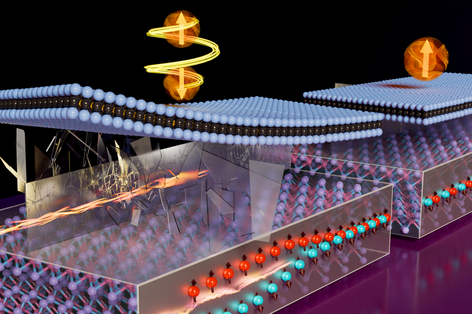
A team of MIT researchers has now achieved this critical milestone by designing a “van der Waals atomically layered heterostructure” device where a 2D van der Waals magnet, iron gallium telluride, is interfaced with another 2D material, tungsten ditelluride. In an open-access paper published March 15 in Science Advances, the team shows that the magnet can be toggled between the 0 and 1 states simply by applying pulses of electrical current across their two-layer device.
“Our device enables robust magnetization switching without the need for an external magnetic field, opening up unprecedented opportunities for ultra-low power and environmentally sustainable computing technology for big data and AI,” says lead author Deblina Sarkar, the AT&T Career Development Assistant Professor at the MIT Media Lab and Center for Neurobiological Engineering, and head of the Nano-Cybernetic Biotrek research group. “Moreover, the atomically layered structure of our device provides unique capabilities including improved interface and possibilities of gate voltage tunability, as well as flexible and transparent spintronic technologies.”
Sarkar is joined on the paper by first author Shivam Kajale, a graduate student in Sarkar’s research group at the Media Lab; Thanh Nguyen, a graduate student in the Department of Nuclear Science and Engineering (NSE); Nguyen Tuan Hung, an MIT visiting scholar in NSE and an assistant professor at Tohoku University in Japan; and Mingda Li, associate professor of NSE.
Breaking the mirror symmetries
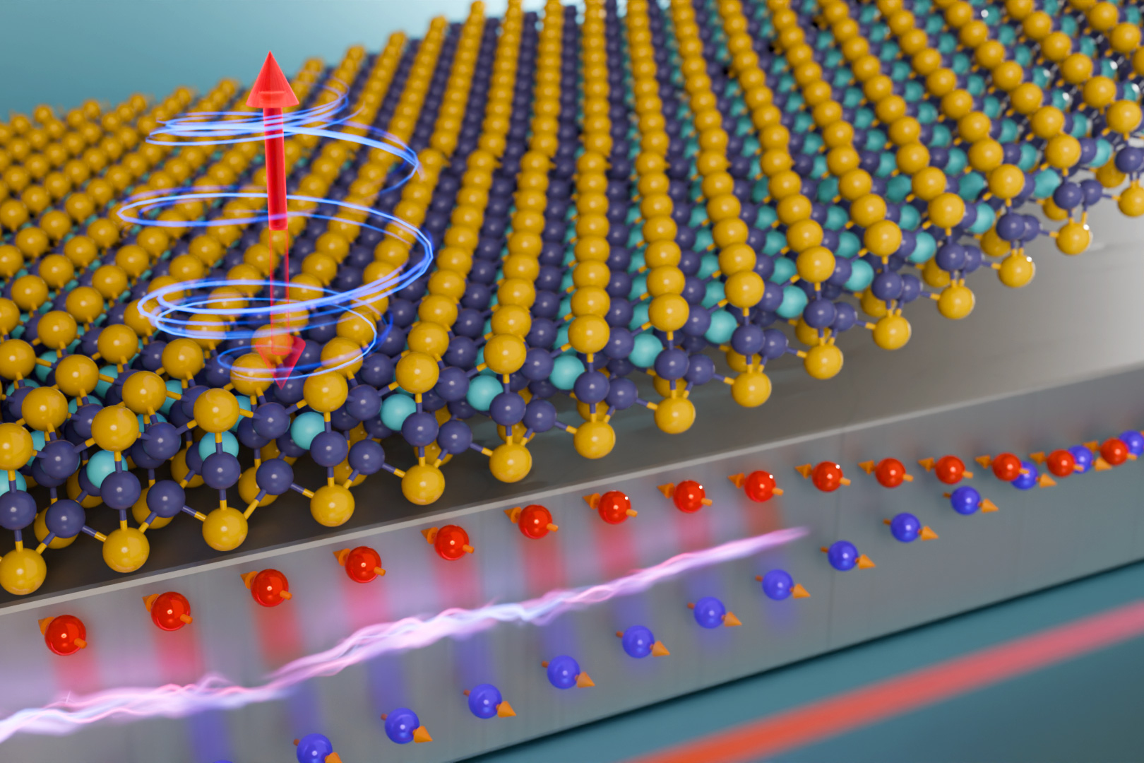
When electric current flows through heavy metals like platinum or tantalum, the electrons get segregated in the materials based on their spin component, a phenomenon called the spin Hall effect, says Kajale. The way this segregation happens depends on the material, and particularly its symmetries.
“The conversion of electric current to spin currents in heavy metals lies at the heart of controlling magnets electrically,” Kajale notes. “The microscopic structure of conventionally used materials, like platinum, have a kind of mirror symmetry, which restricts the spin currents only to in-plane spin polarization.”
Kajale explains that two mirror symmetries must be broken to produce an “out-of-plane” spin component that can be transferred to a magnetic layer to induce field-free switching. “Electrical current can 'break' the mirror symmetry along one plane in platinum, but its crystal structure prevents the mirror symmetry from being broken in a second plane.”
In their earlier experiments, the researchers used a small magnetic field to break the second mirror plane. To get rid of the need for a magnetic nudge, Kajale and Sarkar and colleagues looked instead for a material with a structure that could break the second mirror plane without outside help. This led them to another 2D material, tungsten ditelluride. The tungsten ditelluride that the researchers used has an orthorhombic crystal structure. The material itself has one broken mirror plane. Thus, by applying current along its low-symmetry axis (parallel to the broken mirror plane), the resulting spin current has an out-of-plane spin component that can directly induce switching in the ultra-thin magnet interfaced with the tungsten ditelluride.
“Because it's also a 2D van der Waals material, it can also ensure that when we stack the two materials together, we get pristine interfaces and a good flow of electron spins between the materials,” says Kajale.
Becoming more energy-efficient
Computer memory and processors built from magnetic materials use less energy than traditional silicon-based devices. And the van der Waals magnets can offer higher energy efficiency and better scalability compared to bulk magnetic material, the researchers note.
The electrical current density used for switching the magnet translates to how much energy is dissipated during switching. A lower density means a much more energy-efficient material. “The new design has one of the lowest current densities in van der Waals magnetic materials,” Kajale says. “This new design has an order of magnitude lower in terms of the switching current required in bulk materials. This translates to something like two orders of magnitude improvement in energy efficiency.”
The research team is now looking at similar low-symmetry van der Waals materials to see if they can reduce current density even further. They are also hoping to collaborate with other researchers to find ways to manufacture the 2D magnetic switch devices at commercial scale.
This work was carried out, in part, using the facilities at MIT.nano. It was funded by the Media Lab, the U.S. National Science Foundation, and the U.S. Department of Energy.
![]()
© Image courtesy of the researchers.


