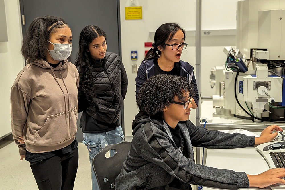
Researchers demonstrate the first chip-based 3D printer
Imagine a portable 3D printer you could hold in the palm of your hand. The tiny device could enable a user to rapidly create customized, low-cost objects on the go, like a fastener to repair a wobbly bicycle wheel or a component for a critical medical operation.
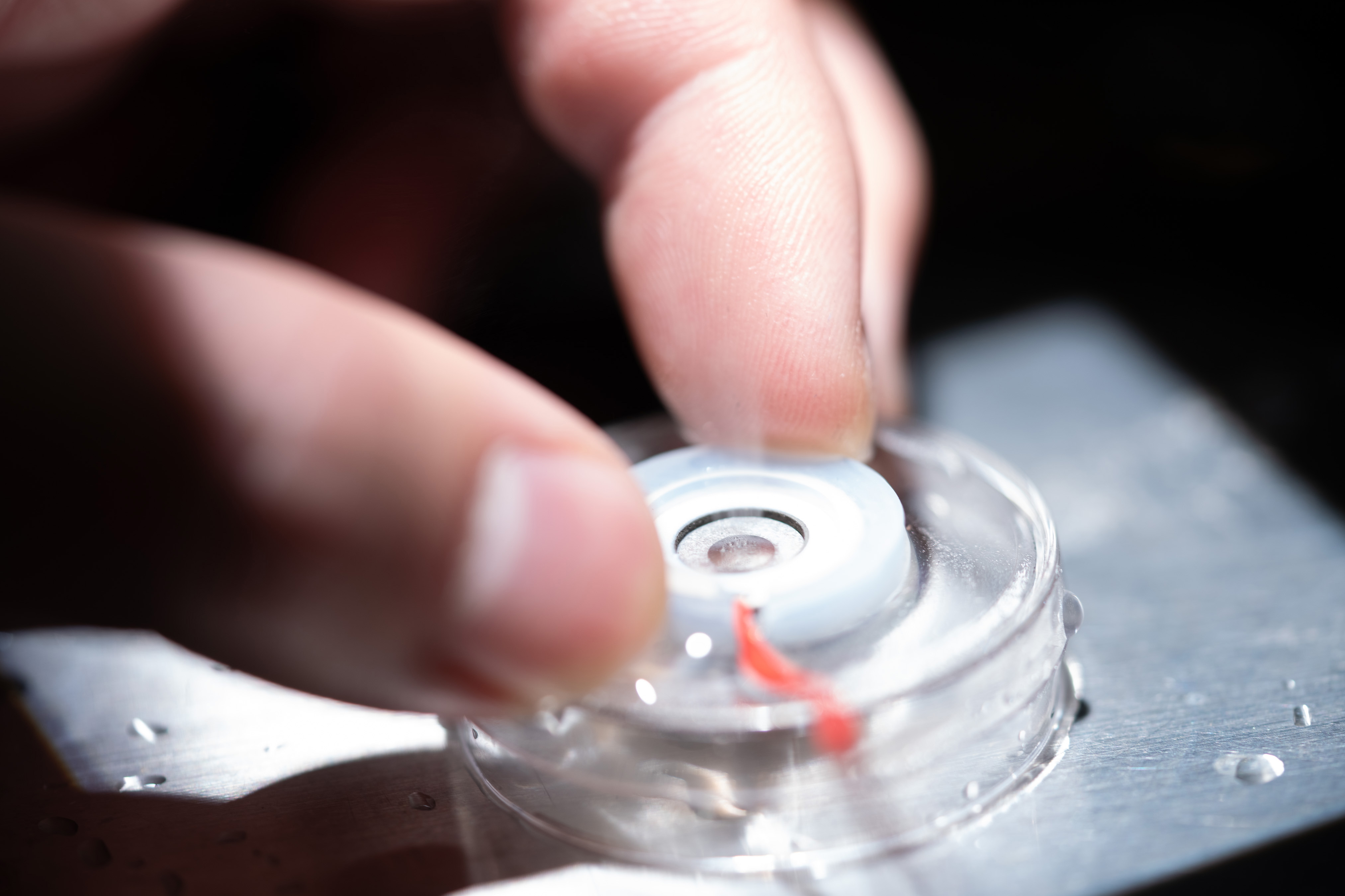
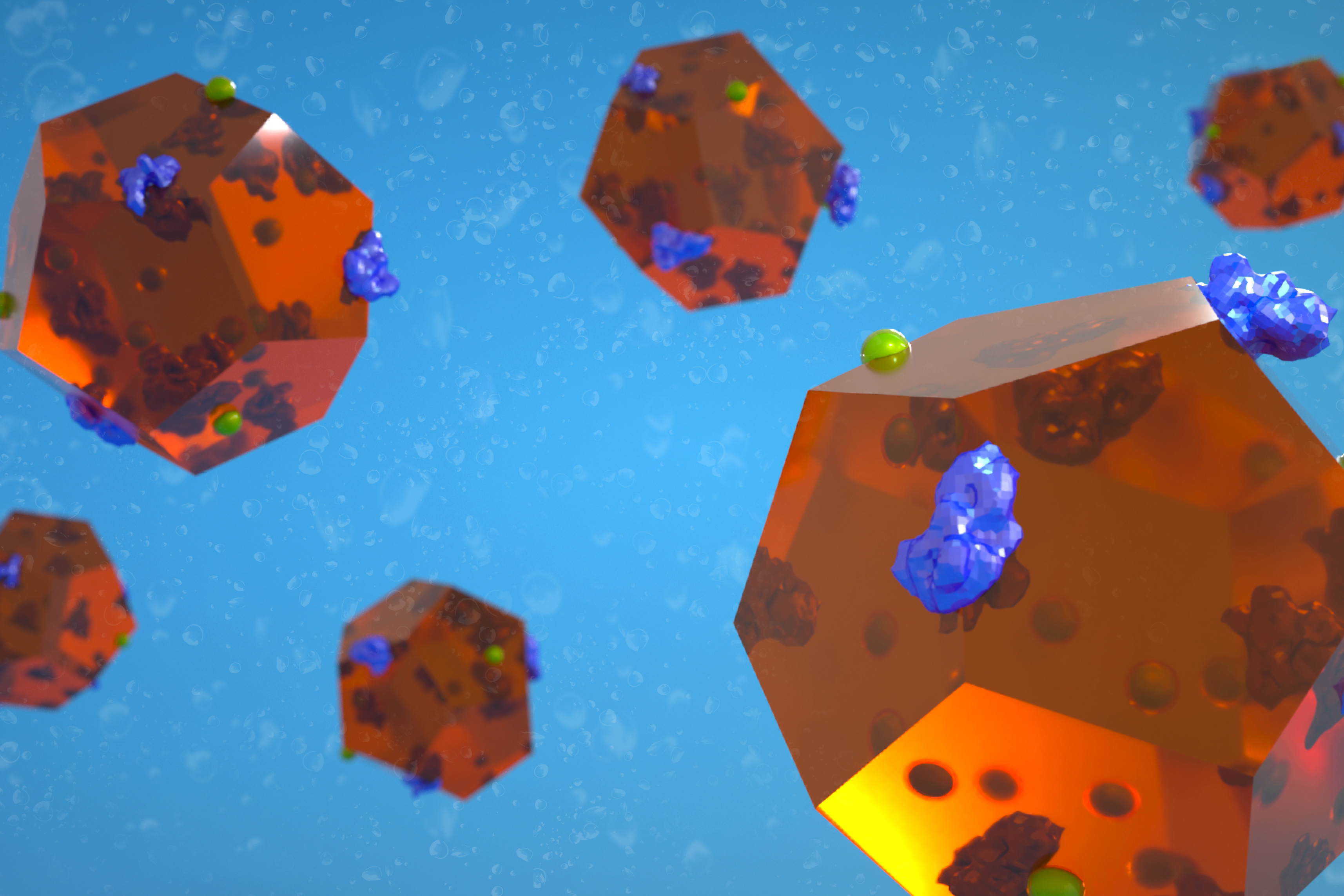
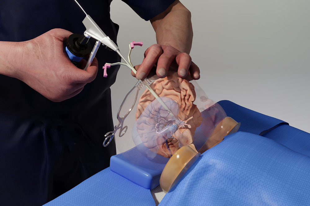
Researchers from MIT and the University of Texas at Austin took a major step toward making this idea a reality by demonstrating the first chip-based 3D printer. Their proof-of-concept device consists of a single, millimeter-scale photonic chip that emits reconfigurable beams of light into a well of resin that cures into a solid shape when light strikes it.
The prototype chip has no moving parts, instead relying on an array of tiny optical antennas to steer a beam of light. The beam projects up into a liquid resin that has been designed to rapidly cure when exposed to the beam’s wavelength of visible light.
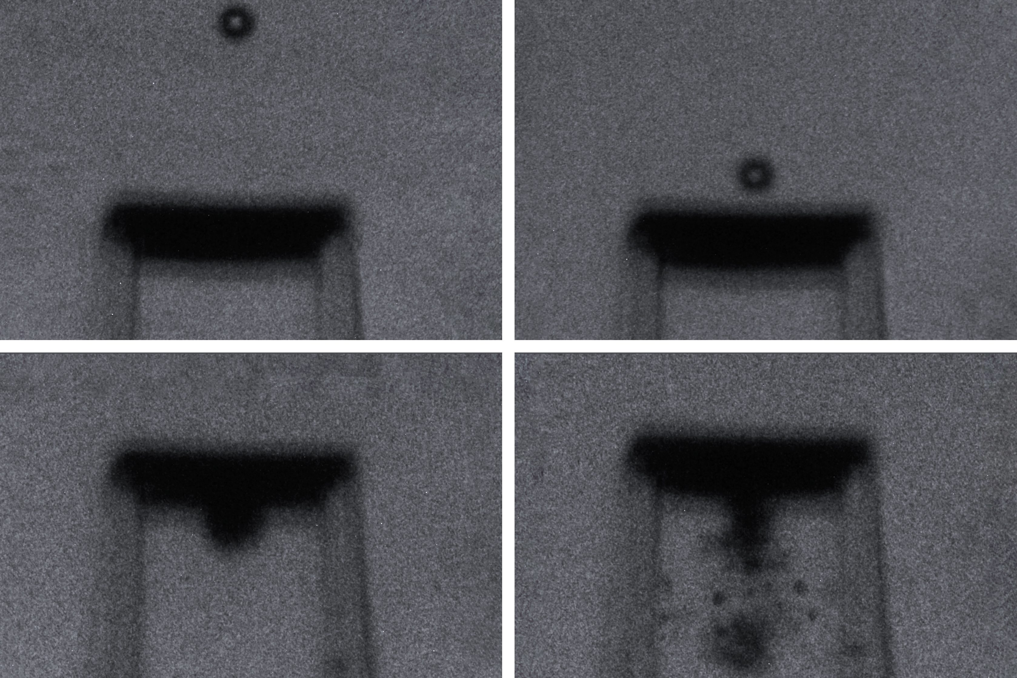
By combining silicon photonics and photochemistry, the interdisciplinary research team was able to demonstrate a chip that can steer light beams to 3D print arbitrary two-dimensional patterns, including the letters M-I-T. Shapes can be fully formed in a matter of seconds.
In the long run, they envision a system where a photonic chip sits at the bottom of a well of resin and emits a 3D hologram of visible light, rapidly curing an entire object in a single step.
This type of portable 3D printer could have many applications, such as enabling clinicians to create tailor-made medical device components or allowing engineers to make rapid prototypes at a job site.
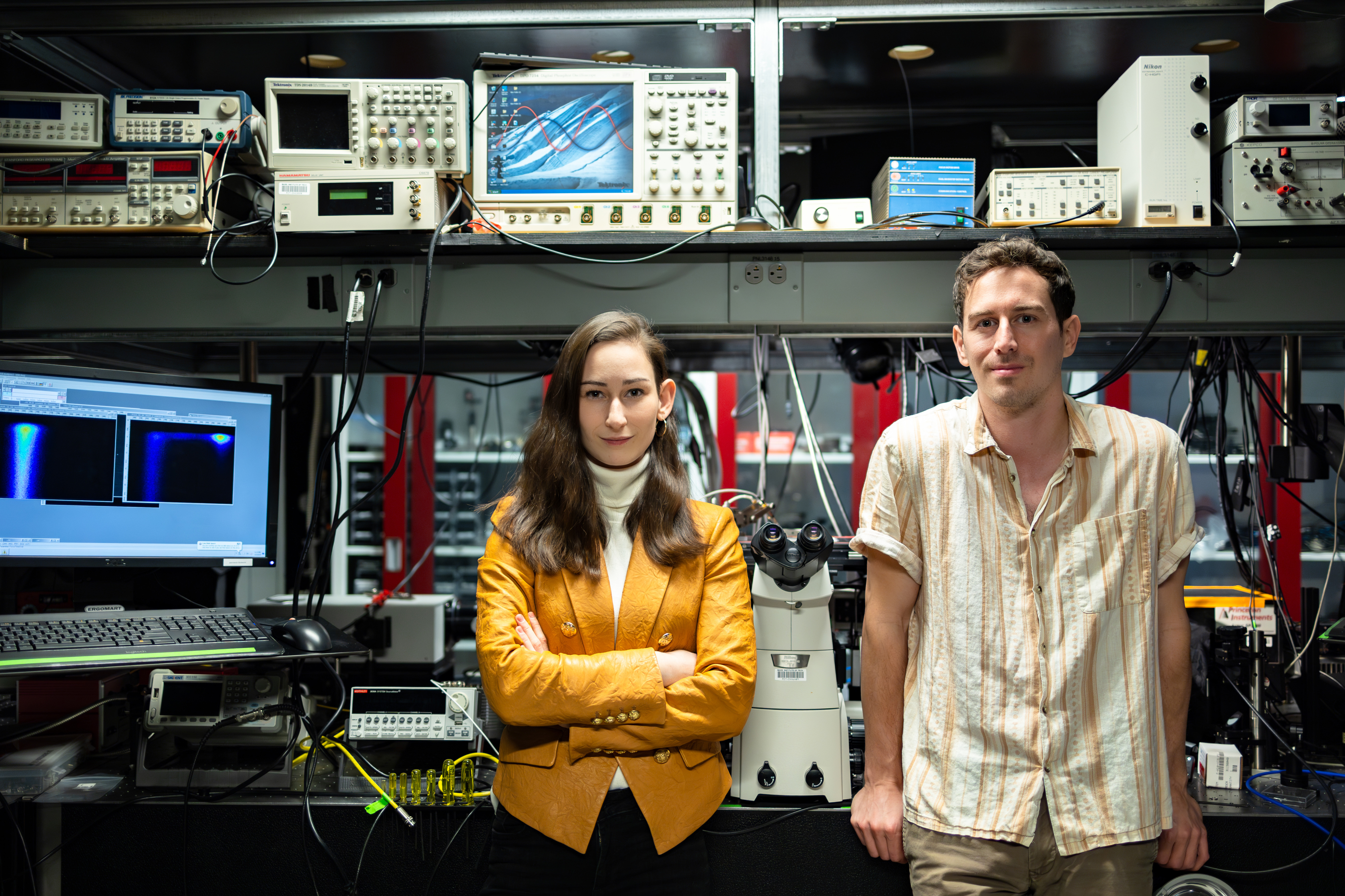
“This system is completely rethinking what a 3D printer is. It is no longer a big box sitting on a bench in a lab creating objects, but something that is handheld and portable. It is exciting to think about the new applications that could come out of this and how the field of 3D printing could change,” says senior author Jelena Notaros, the Robert J. Shillman Career Development Professor in Electrical Engineering and Computer Science (EECS), and a member of the Research Laboratory of Electronics.
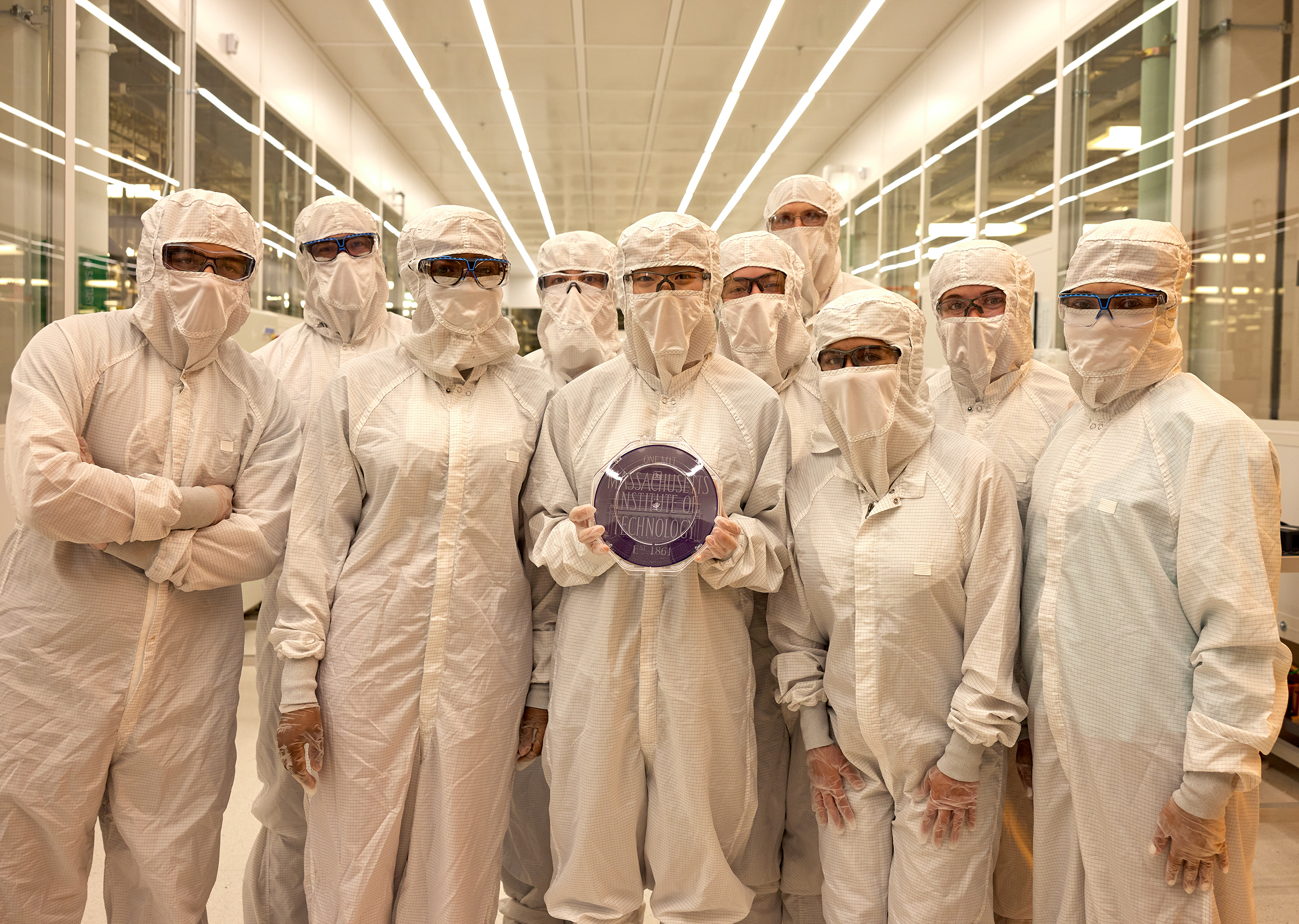
Joining Notaros on the paper are Sabrina Corsetti, lead author and EECS graduate student; Milica Notaros PhD ’23; Tal Sneh, an EECS graduate student; Alex Safford, a recent graduate of the University of Texas at Austin; and Zak Page, an assistant professor in the Department of Chemical Engineering at UT Austin. The research appears today in Nature Light Science and Applications.
Printing with a chip
Experts in silicon photonics, the Notaros group previously developed integrated optical-phased-array systems that steer beams of light using a series of microscale antennas fabricated on a chip using semiconductor manufacturing processes. By speeding up or delaying the optical signal on either side of the antenna array, they can move the beam of emitted light in a certain direction.
Such systems are key for lidar sensors, which map their surroundings by emitting infrared light beams that bounce off nearby objects. Recently, the group has focused on systems that emit and steer visible light for augmented-reality applications.
They wondered if such a device could be used for a chip-based 3D printer.
At about the same time they started brainstorming, the Page Group at UT Austin demonstrated specialized resins that can be rapidly cured using wavelengths of visible light for the first time. This was the missing piece that pushed the chip-based 3D printer into reality.
“With photocurable resins, it is very hard to get them to cure all the way up at infrared wavelengths, which is where integrated optical-phased-array systems were operating in the past for lidar,” Corsetti says. “Here, we are meeting in the middle between standard photochemistry and silicon photonics by using visible-light-curable resins and visible-light-emitting chips to create this chip-based 3D printer. You have this merging of two technologies into a completely new idea.”
Their prototype consists of a single photonic chip containing an array of 160-nanometer-thick optical antennas. (A sheet of paper is about 100,000 nanometers thick.) The entire chip fits onto a U.S. quarter.
When powered by an off-chip laser, the antennas emit a steerable beam of visible light into the well of photocurable resin. The chip sits below a clear slide, like those used in microscopes, which contains a shallow indentation that holds the resin. The researchers use electrical signals to nonmechanically steer the light beam, causing the resin to solidify wherever the beam strikes it.
A collaborative approach
But effectively modulating visible-wavelength light, which involves modifying its amplitude and phase, is especially tricky. One common method requires heating the chip, but this is inefficient and takes a large amount of physical space.
Instead, the researchers used liquid crystal to fashion compact modulators they integrate onto the chip. The material’s unique optical properties enable the modulators to be extremely efficient and only about 20 microns in length.
A single waveguide on the chip holds the light from the off-chip laser. Running along the waveguide are tiny taps which tap off a little bit of light to each of the antennas.
The researchers actively tune the modulators using an electric field, which reorients the liquid crystal molecules in a certain direction. In this way, they can precisely control the amplitude and phase of light being routed to the antennas.
But forming and steering the beam is only half the battle. Interfacing with a novel photocurable resin was a completely different challenge.
The Page Group at UT Austin worked closely with the Notaros Group at MIT, carefully adjusting the chemical combinations and concentrations to zero-in on a formula that provided a long shelf-life and rapid curing.
In the end, the group used their prototype to 3D print arbitrary two-dimensional shapes within seconds.
Building off this prototype, they want to move toward developing a system like the one they originally conceptualized — a chip that emits a hologram of visible light in a resin well to enable volumetric 3D printing in only one step.
“To be able to do that, we need a completely new silicon-photonics chip design. We already laid out a lot of what that final system would look like in this paper. And, now, we are excited to continue working towards this ultimate demonstration,” Jelena Notaros says.
This work was funded, in part, by the U.S. National Science Foundation, the U.S. Defense Advanced Research Projects Agency, the Robert A. Welch Foundation, the MIT Rolf G. Locher Endowed Fellowship, and the MIT Frederick and Barbara Cronin Fellowship.
![]()
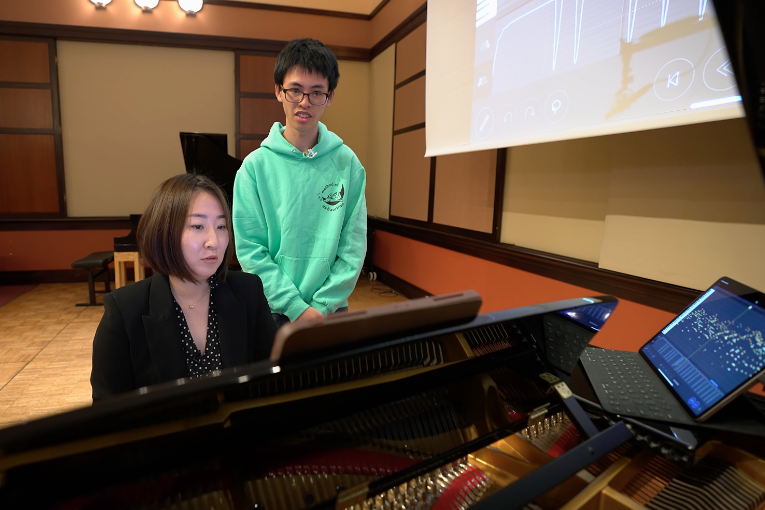
© Credit: Sampson Wilcox, RLE