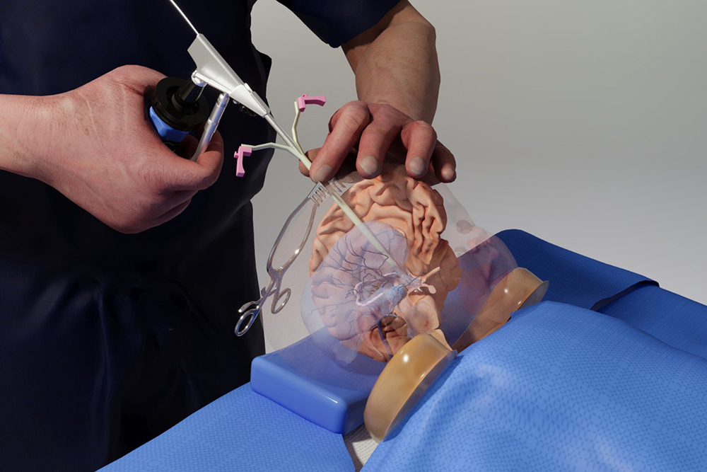
Brain surgery training from an avatar
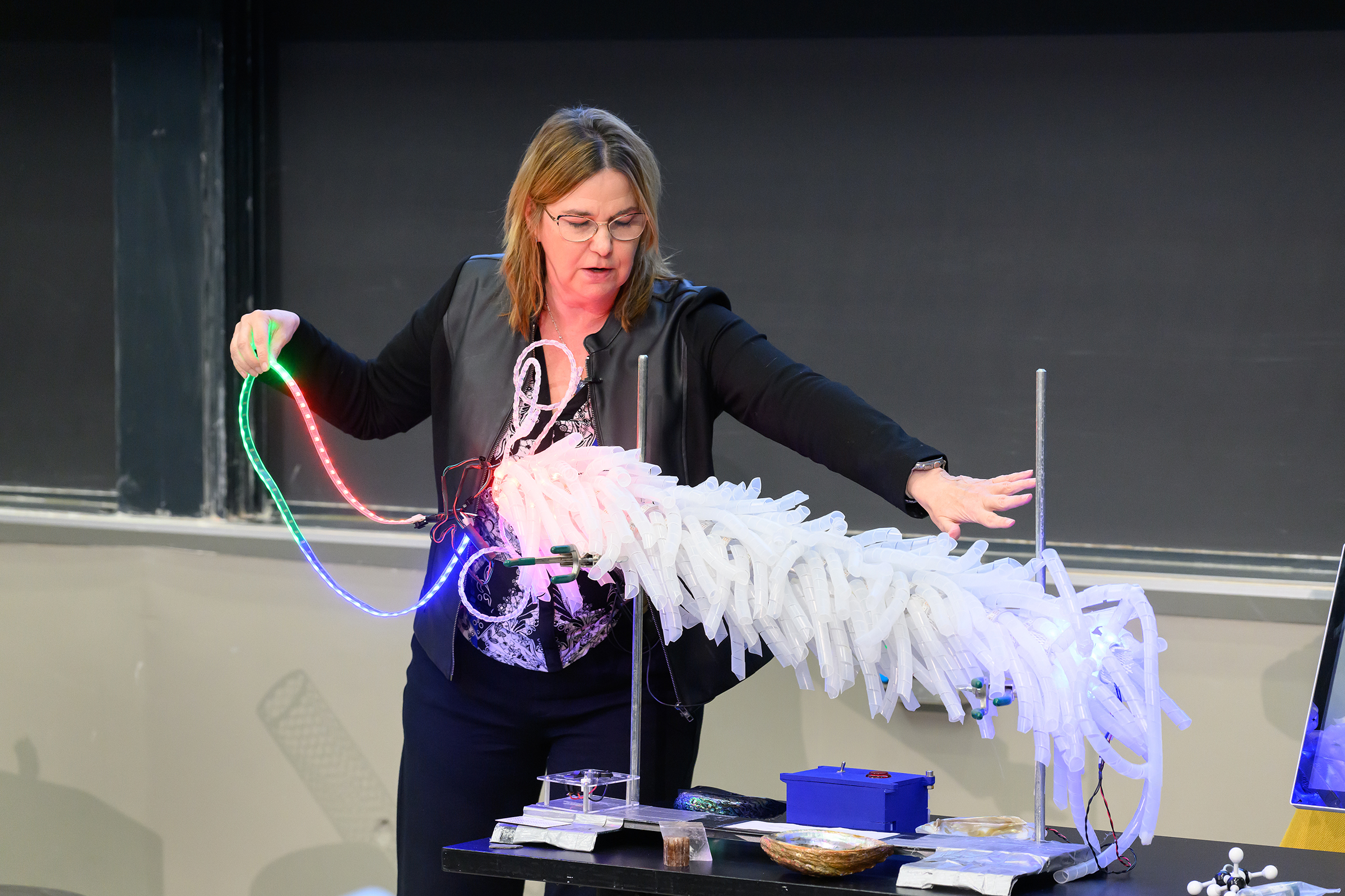
Benjamin Warf, a renowned neurosurgeon at Boston Children’s Hospital, stands in the MIT.nano Immersion Lab. More than 3,000 miles away, his virtual avatar stands next to Matheus Vasconcelos in Brazil as the resident practices delicate surgery on a doll-like model of a baby’s brain.
With a pair of virtual-reality goggles, Vasconcelos is able to watch Warf’s avatar demonstrate a brain surgery procedure before replicating the technique himself and while asking questions of Warf’s digital twin.
“It’s an almost out-of-body experience,” Warf says of watching his avatar interact with the residents. “Maybe it’s how it feels to have an identical twin?”
And that’s the goal: Warf’s digital twin bridged the distance, allowing him to be functionally in two places at once. “It was my first training using this model, and it had excellent performance,” says Vasconcelos, a neurosurgery resident at Santa Casa de São Paulo School of Medical Sciences in São Paulo, Brazil. “As a resident, I now feel more confident and comfortable applying the technique in a real patient under the guidance of a professor.”
Warf’s avatar arrived via a new project launched by medical simulator and augmented reality (AR) company EDUCSIM. The company is part of the 2023 cohort of START.nano, MIT.nano’s deep-tech accelerator that offers early-stage startups discounted access to MIT.nano’s laboratories.
In March 2023, Giselle Coelho, EDUCSIM’s scientific director and a pediatric neurosurgeon at Santa Casa de São Paulo and Sabará Children’s Hospital, began working with technical staff in the MIT.nano Immersion Lab to create Warf’s avatar. By November, the avatar was training future surgeons like Vasconcelos.
“I had this idea to create the avatar of Dr. Warf as a proof of concept, and asked, ‘What would be the place in the world where they are working on technologies like that?’” Coelho says. “Then I found MIT.nano.”
Capturing a Surgeon
As a neurosurgery resident, Coelho was so frustrated by the lack of practical training options for complex surgeries that she built her own model of a baby brain. The physical model contains all the structures of the brain and can even bleed, “simulating all the steps of a surgery, from incision to skin closure,” she says.
She soon found that simulators and virtual reality (VR) demonstrations reduced the learning curve for her own residents. Coelho launched EDUCSIM in 2017 to expand the variety and reach of the training for residents and experts looking to learn new techniques.
Those techniques include a procedure to treat infant hydrocephalus that was pioneered by Warf, the director of neonatal and congenital neurosurgery at Boston Children’s Hospital. Coelho had learned the technique directly from Warf and thought his avatar might be the way for surgeons who couldn’t travel to Boston to benefit from his expertise.
To create the avatar, Coelho worked with Talis Reks, the AR/VR/gaming/big data IT technologist in the Immersion Lab.
“A lot of technology and hardware can be very expensive for startups to access as they start their company journey,” Reks explains. “START.nano is one way of enabling them to utilize and afford the tools and technologies we have at MIT.nano’s Immersion Lab.”
Coelho and her colleagues needed high-fidelity and high-resolution motion-capture technology, volumetric video capture, and a range of other VR/AR technologies to capture Warf’s dexterous finger motions and facial expressions. Warf visited MIT.nano on several occasions to be digitally “captured,” including performing an operation on the physical baby model while wearing special gloves and clothing embedded with sensors.
“These technologies have mostly been used for entertainment or VFX [visual effects] or CGI [computer-generated imagery],” says Reks, “But this is a unique project, because we’re applying it now for real medical practice and real learning.”
One of the biggest challenges, Reks says, was helping to develop what Coelho calls “holoportation”— transmitting the 3D, volumetric video capture of Warf in real-time over the internet so that his avatar can appear in transcontinental medical training.
The Warf avatar has synchronous and asynchronous modes. The training that Vasconcelos received was in the asynchronous mode, where residents can observe the avatar’s demonstrations and ask it questions. The answers, delivered in a variety of languages, come from AI algorithms that draw from previous research and an extensive bank of questions and answers provided by Warf.
In the synchronous mode, Warf operates his avatar from a distance in real time, Coelho says. “He could walk around the room, he could talk to me, he could orient me. It’s amazing.”
Coelho, Warf, Reks, and other team members demonstrated a combination of the modes in a second session in late December. This demo consisted of volumetric live video capture between the Immersion Lab and Brazil, spatialized and visible in real-time through AR headsets. It significantly expanded upon the previous demo, which had only streamed volumetric data in one direction through a two-dimensional display.
Powerful impacts
Warf has a long history of training desperately needed pediatric neurosurgeons around the world, most recently through his nonprofit Neurokids. Remote and simulated training has been an increasingly large part of training since the pandemic, he says, although he doesn’t feel it will ever completely replace personal hands-on instruction and collaboration.
“But if in fact one day we could have avatars, like this one from Giselle, in remote places showing people how to do things and answering questions for them, without the cost of travel, without the time cost and so forth, I think it could be really powerful,” Warf says.
The avatar project is especially important for surgeons serving remote and underserved areas like the Amazon region of Brazil, Coelho says. “This is a way to give them the same level of education that they would get in other places, and the same opportunity to be in touch with Dr. Warf.”
One baby treated for hydrocephalus at a recent Amazon clinic had traveled by boat 30 hours for the surgery, according to Coelho.
Training surgeons with the avatar, she says, “can change reality for this baby and can change the future.”
![]()
© Photo courtesy of the MIT.nano Immersion Lab.