FreshRSS

Normální zobrazení

Jsou dostupné nové články, klikněte pro obnovení stránky.
PředevčíremMIT News - Nanoscience and nanotechnology | MIT.nano

MIT spinout Arnasi begins applying LiquiGlide no-stick technology to help patients

The no-stick technology invented by Professor Kripa Varanasi and David Smith SM ’11, initially commercialized as LiquiGlide in 2012, went viral for its uncanny ability to make materials that stick to their containers — think ketchup, cosmetics, and toothpaste — slide out with ease.

Now, the company that brought you Colgate no-stick toothpaste is moving into the medical space, and the applications could improve millions of lives. The company, which recently rebranded as the Arnasi Group, has developed an ambitious plan to launch three new biomedical products over the next four years.

The first of those products, called Revel, is a deodorizing lubricant designed for ostomy pouches, which are used by individuals to collect bodily waste after digestive system surgeries. Up to 1 million people rely on such pouches in the United States. Ostomy pouches must be emptied multiple times per day, and issues resulting from sticking or clogging can cause embarrassing, time-consuming situations for the people relying on them.

Arnasi’s deodorizing lubricant can prevent clogging and simplify the ostomy pouch cleaning process. Unlike other options available, one application of its lubricant works for the entire day, the Arnasi team says, and they designed a single unit dose that fits in your pocket for added convenience.

An ostomy pouch “significantly impacts a person’s lifestyle,” Varanasi says. “They need to keep it clean, and they need to use it at all times. We are solving a very important problem while helping people by giving their dignity and lifestyles back.”

Revel, Arnasi’s FDA-registered product, officially launched this month, and it has already received promising feedback from nurses and patients.

Margaret is a nurse who relies on an ostomy pouch herself and cares for patients who need them after receiving colostomies and ileostomies. She received samples of Revel at a recent conference and says it could dramatically improve both her and her patients’ lives.

“These pouches need to be emptied frequently, and sometimes that’s very difficult to do,” she says. “This particular product makes everything slide out without any problems at all, and it’s a wonderful improvement. It also lasts long enough to empty the pouch three to four times, which is great because you don’t have to carry a bunch of this stuff around.”

Margaret’s experience echoes feedback Arnasi’s team has heard from many others.

“When we showed it to the nurses, they were blown away with the product,” says Arnasi CEO Dan Salain. “They asked us to get this product out to the market as fast as we could, and so that’s what we’re doing.”

Arnasi’s next medical products will be used to prevent biofilm and bacterial infections caused by implants and catheters, and will also help people with cystic fibrosis.

“We want to create products that really help people,” Salain says. “Anything that’s implantable in the body, whether it’s a catheter, a hip, knee, or joint replacement, a breast implant, a bladder sling — those things lend themselves to our technology.”

From packages to patients

Varanasi initially developed Arnasi’s liquid-impregnated surface technology with Smith, Arnasi’s co-founder and current CTO, when Smith was a graduate student in Varanasi’s lab. The research was initially funded by the MIT Energy Initiative and the MIT Deshpande Center to work on solid-liquid interfaces with broad applications for energy, water, and more.

“There’s this fundamental friction constraint called the no-slip boundary condition between a liquid and a solid, so by creating a new surface in which we can infuse a liquid that is less viscous, we can now get the product to easily slide on surfaces,” Varanasi explains. “That aha moment meant we could get around a fundamental constraint in fluid dynamics.”

Still, sticky surfaces are everywhere, and the scientific co-founders had to decide where to apply their technology first. Shortly after the invention, Varanasi was at home trying to decide on the best application when he saw his wife across the kitchen table trying to get honey out of a bottle. It was another aha moment.

Soon after, Varanasi’s team entered the MIT $100K Entrepreneurship Competition. The competition — and the corresponding videos of ketchup and other materials sliding out their bottles with ease — created a media storm and a frenzy of attention.

“The press exploded,” Varanasi says. “For three months, my phone didn’t stop ringing. My group website crashed. There was a lot of market pull and in response, we founded the company.”

Arnasi, still operating as LiquiGlide, licensed the intellectual property from MIT’s Technology Licensing Office and eventually signed large deals with some of the world’s biggest consumer packaged goods companies, who used it to create products like fully recyclable toothpaste.

“There is so much waste just because we can't get all of the product, be it food, cosmetics, or medical products, out of containers,” Varanasi says. “Fifty billion-plus packages are sold every year, and 5 to 10 percent of product is left behind on average. So, you can imagine the CO2 footprint of the wasted product. And even though a lot of this is in recyclable packaging, they can’t be recycled because you need to wash out all the product. The water footprint of this is huge, not to mention the wasted product.”

While all of that was going on, Arnasi’s team was also looking into the biomedical space. For instance, Varanasi’s lab previously showed the technology could be used to prevent occlusion from blood clots and thrombosis and reduce biofilm formation, among other applications.

After studying the industry and speaking with patients and nurses, Arnasi realized a better lubricant for ostomy pouches could improve millions of people’s lives.

“Stool accumulates in these pouches outside of people’s bodies, and they need to empty it up to eight times a day,” explains Brienne Engel, Arnasi’s director of business development. “That process has a lot of challenges associated with it: It can be difficult to drain, leaving a lot of mass behind, it takes a long time to drain, so you can spend a long time in a restroom trying to clear out your pouch, and then there’s something called pancaking that can push the pouch off the [surgical opening], introducing issues like leakage, odor, and failure of the ostomy pouching system.”

Ostomy and beyond

Arnasi’s ostomy lubricant, Revel, is the first non-water-based solution on the market, and as-yet unpublished third-party testing has shown it allows for faster, more complete pouch drainage, along with other benefits.

“A lot of the existing brands treat their consumers like patients, but what we’ve found is they want to be treated like people and have a consumer experience,” Salain says. “The magic we saw with our toothpaste product was people got this amazing consumer experience out of it, and we wanted to create the same thing with Revel.”

Now Arnasi is planning to use its technology in medical products for skin infections, cystic fibrosis, and in implantable catheters and joint replacements. Arnasi’s team believes those last two use cases could prevent millions of deadly infections.

“When people are getting hemodialysis catheters, they have a 33 percent risk of developing infections, and those that do get those infections have a 25 percent chance of dying from them,” Engel says. “Taking our underlying technology and applying it to catheters, for example, imparts anti-biofilm properties and also prevent things like thrombosis, or blood clotting on the outside of these catheters, which is a problem in and of itself but also provides a space for bacteria to seed.”

Ultimately, Varanasi’s team is balancing making progress on its biomedical applications while exploring other avenues for its technology — including energy, manufacturing, and agriculture — to maximize its impact on the world.

“We think of this as a company with many companies within it because of all the different areas that it can impact. Liquid-solid interfaces are ubiquitous, viscous products are everywhere, and deploying this technology to solve difficult problems has been a dream,” Varanasi says. “It’s a great example of how MIT technology can be used for the benefit of humankind.”

© Image: Courtesy of Liquiglide

“[B]y creating a new surface in which we can infuse a liquid that is less viscous, we can now get the product to easily slide on surfaces,” Varanasi explains.
Professor Emeritus John Vander Sande, microscopist, entrepreneur, and admired mentor, dies at 80

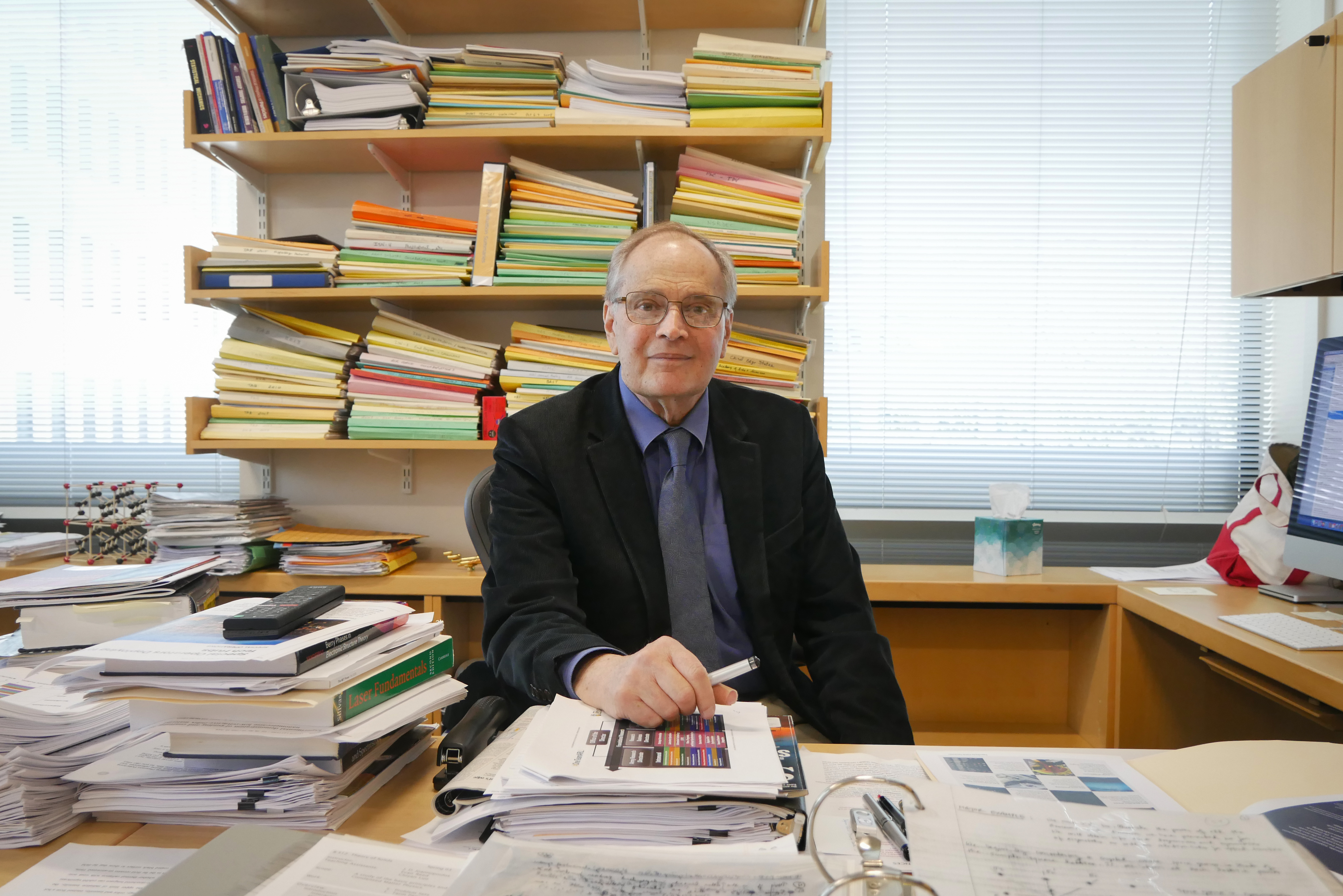
MIT Professor Emeritus John B. Vander Sande, a pioneer in electron microscopy and beloved educator and advisor known for his warmth and empathetic instruction, died June 28 in Newbury, Massachusetts. He was 80.

The Cecil and Ida Green Distinguished Professor in the Department of Materials Science and Engineering (DMSE), Vander Sande was a physical metallurgist, studying the physical properties and structure of metals and alloys. His long career included a major entrepreneurial pursuit, launching American Superconductor; forming international academic partnerships; and serving in numerous administrative roles at MIT and, after his retirement, one in Iceland.

Vander Sande’s interests encompassed more than science and technology; a self-taught scholar on 17th- and 18th-century furniture, he boasts a production credit in the 1996 film “The Crucible.”

He is perhaps best remembered for bringing the first scanning transmission electron microscope (STEM) into the United States. This powerful microscope uses a beam of electrons to scan material samples and investigate their structure and composition.

“John was the person who really built up what became MIT’s modern microscopy expertise,” says Samuel M. Allen, the POSCO Professor Emeritus of Physical Metallurgy. Vander Sande studied electron microscopy during a postdoctoral fellowship at Oxford University in England with luminaries Sir Peter Hirsch and Colin Humphreys. “The people who wrote the first book on transmission electron microscopy were all there at Oxford, and John basically brought that expertise to MIT in his teaching and mentoring.”

Born in Baltimore, Maryland, in 1944, Vander Sande grew up in Westwood, New Jersey. He studied mechanical engineering at Stevens Institute of Technology, earning a bachelor’s degree in 1966, and switched to materials science and engineering at Northwestern University, receiving a PhD in 1970. Following his time at Oxford, Vander Sande joined MIT as assistant professor in 1971.

A vision for advanced microscopy

At MIT, Vander Sande became known as a leading practitioner of weak-beam microscopy, a technique refined by Hirsch to improve images of dislocations, tiny imperfections in crystalline materials that help researchers determine why materials fail.

His procurement of the STEM instrument from the U.K. company Vacuum Generators in the mid-1970s was a substantial innovation, allowing researchers to visualize individual atoms and identify chemical elements in materials.

“He showed the capabilities of new techniques, like scanning transmission electron microscopy, in understanding the physics and chemistry of materials at the nanoscale,” says Yet-Ming Chiang, the Kyocera Professor of Ceramics at DMSE. Today, MIT.nano stands as one of the world’s foremost facilities for advanced microscopy techniques. “He paved the way, at MIT, certainly, and more broadly, to those state-of-the-art instruments that we have today.”

The director of a microscopy laboratory at MIT, Vander Sande used instruments like that early STEM and its successors to study how manufacturing processes affect material structure and properties.

One focus was rapid solidification, which involves cooling materials quickly to enhance their properties. Tom Kelly, a PhD student in the late 1970s, worked with Vander Sande to explore how fast-cooling molten metal as powder changes its internal structure. They discovered that “precipitates,” or small particles formed during the rapid cooling, made the metal stronger.

“It took me at least a year to finally get some success. But we did succeed,” says Kelly, CEO of STEAM Instruments, a startup that is developing mass spectrometry technology, which measures and analyzes atoms emitted by substances. “That was John who brought that project and the solution to the table.”

Using his deep expertise in metals and other materials, including superconducting oxides, which can conduct electricity when cooled to low temperatures, Vander Sande co-founded American Superconductor with fellow DMSE faculty member Greg Yurek in 1987. The company produced high-temperature superconducting wires now used in renewable energy technology.

“In the MIT entrepreneurial ecosystem, American Superconductor was a pioneer,” says Chiang, who was part of the startup’s co-founding membership. “It was one of the early companies that was formed on the basis of research at MIT, in which faculty spun out a company, as opposed to graduates starting companies.”

To teach them is to know them

While Yurek left MIT to lead the American Superconductor full time as CEO, Vander Sande stayed on the faculty at DMSE, remaining a consultant to the company and board member for many years.

That comes as no surprise to his students, who recall a passionate and devoted educator and mentor.

“He was a terrific teacher,” says Frank Gayle, a former PhD student of Vander Sande’s who recently retired from his job as director at the National Institute of Standards and Technology. “He would take the really complex subjects, super mathematical and complicated, and he would teach them in a way that you felt comfortable as a student learning them. He really had a terrific knack for that.”

Chiang said Vander Sande was an “exceptionally clear” lecturer who would use memorable imagery to get concepts across, like comparing heterogenous nanoparticles, tiny particles that have a varied structure or composition, to a black-and-white Holstein cow. “Hard to forget,” Chiang says.

Powering Vander Sande’s teaching, Gayle said, was an aptitude for knowing the people he was teaching, for recognizing their backgrounds and what they knew and didn’t know. He likened Vander Sande to a dad on Take Your Kid to Work Day, demystifying an unfamiliar world. “He had some way of doing that, and then he figured out how to get the pieces together to make it comprehensible.”

He brought a similar talent to mentorship, with an emphasis on the individual rather than the project, Gayle says. “He really worked with people to encourage them to do creative things and encouraged their creativity.”

Kelly, who was a University of Wisconsin professor before becoming a repeat entrepreneur, says Vander Sande was an exceptional role model for young grad students.

“When you see these people who’ve accomplished a lot, you’re afraid to even talk to them,” he says. “But in reality, they’re regular people. One of the things I learned from John was that he’s just a regular person who does good work. I realized that, Hey, I can be a regular person and do good work, too.”

Another former grad student, Matt Libera, says he learned as much about life from Vander Sande as he did about materials science and engineering.

“Because he was not just a scientist-engineer, but really a well-rounded human being and shared a lot of experience and advice that went beyond just the science,” says Libera, a materials science and engineering professor at Stevens Institute of Technology, Vander Sande’s alma mater.

“A rare talent”

Vander Sande was equally dedicated to MIT and his department. In DMSE, he was on multiple committees, on undergraduates and curriculum development, and in 1991 he was appointed associate dean of the School of Engineering. He served in the position until 1999, taking over as acting dean twice.

“I remember that that took up a huge amount of his time,” Chiang says. Vander Sande lived in Newbury, Massachusetts, and he and his wife, Marie-Teresa, who long worked for MIT’s Industrial Liaison Program, would travel together to Cambridge by car. “He once told me that he did a lot of the work related to his deanship during that long commute back and forth from Newbury.”

Gayle says Vander Sande’s remarkable communication and people skills are what made him a good fit for leadership roles. “He had a rare talent for those things.”

He also was a bridge from MIT to the rest of the world. Vander Sande played a leading role in establishing the Singapore-MIT Alliance for Research and Technology, a teaching partnership that set up Institute-modeled graduate programs at Singaporean universities. And he was the director of MIT’s half of the Cambridge-MIT Institute, a collaboration with the University of Cambridge in the U.K. that focused on student and faculty exchanges, integrated research, and professional development. Retiring from MIT in 2006, he pursued academic projects in Ecuador, Morocco, and Iceland, and served as acting provost of Reykjavik University from 2009 to 2010.

He had numerous interests outside work, including college football and sports cars, but his greatest passion was for antiques, mainly early American furniture.

A self-taught expert in antiquarian arts, he gave lectures on connoisseurship and attended auctions and antique shows. His interest extended to his home, built in 1697, which had low ceilings that were inconvenient for the 6-foot-1 Vander Sande.

So respected was he for his expertise that the production crew for 20th Century Fox’s “The Crucible” sought him out. The film, about the Salem, Massachusetts, witch trials, was set in 1692. The crew made copies of furniture from his collection, and Vander Sande consulted on set design and decoration to ensure historical accuracy.

His passion extended beyond just historical artifacts, says Professor Emeritus Allen. He was profoundly interested in learning about the people behind them.

“He liked to read firsthand accounts, letters and stuff,” he says. “His real interest was trying to understand how people two centuries ago or more thought, what their lives were like. It wasn’t just that he was an antiques collector.”

Vander Sande is survived by his wife, Marie-Teresa Vander Sande; his son, John Franklin VanderSande, and his wife, Melanie; his daughter, Rosse Marais VanderSande Ellis, and her husband, Zak Ellis; and grandchildren Gabriel Rhys Pelletier, Sophia Marais VanderSande, and John Christian VanderSande.

© Photo courtesy of the DMSE.

MIT Professor Emeritus John B. Vander Sande is credited with bringing the first scanning transmission electron microscope into the United States. This powerful microscope uses a beam of electrons to scan material samples and investigate their structure and composition.

MIT researchers identify routes to stronger titanium alloys

Titanium alloys are essential structural materials for a wide variety of applications, from aerospace and energy infrastructure to biomedical equipment. But like most metals, optimizing their properties tends to involve a tradeoff between two key characteristics: strength and ductility. Stronger materials tend to be less deformable, and deformable materials tend to be mechanically weak.

Now, researchers at MIT, collaborating with researchers at ATI Specialty Materials, have discovered an approach for creating new titanium alloys that can exceed this historical tradeoff, leading to new alloys with exceptional combinations of strength and ductility, which might lead to new applications.

The findings are described in the journal Advanced Materials, in a paper by Shaolou Wei ScD ’22, Professor C. Cem Tasan, postdoc Kyung-Shik Kim, and John Foltz from ATI Inc. The improvements, the team says, arise from tailoring the chemical composition and the lattice structure of the alloy, while also adjusting the processing techniques used to produce the material at industrial scale.

Titanium alloys have been important because of their exceptional mechanical properties, corrosion resistance, and light weight when compared to steels for example. Through careful selection of the alloying elements and their relative proportions, and of the way the material is processed, “you can create various different structures, and this creates a big playground for you to get good property combinations, both for cryogenic and elevated temperatures,” Tasan says.

But that big assortment of possibilities in turn requires a way to guide the selections to produce a material that meets the specific needs of a particular application. The analysis and experimental results described in the new study provide that guidance.

The structure of titanium alloys, all the way down to atomic scale, governs their properties, Tasan explains. And in some titanium alloys, this structure is even more complex, made up of two different intermixed phases, known as the alpha and beta phases.

“The key strategy in this design approach is to take considerations of different scales,” he says. “One scale is the structure of individual crystal. For example, by choosing the alloying elements carefully, you can have a more ideal crystal structure of the alpha phase that enables particular deformation mechanisms. The other scale is the polycrystal scale, that involves interactions of the alpha and beta phases. So, the approach that’s followed here involves design considerations for both.”

In addition to choosing the right alloying materials and proportions, steps in the processing turned out to play an important role. A technique called cross-rolling is another key to achieving the exceptional combination of strength and ductility, the team found.

Working together with ATI researchers, the team tested a variety of alloys under a scanning electron microscope as they were being deformed, revealing details of how their microstructures respond to external mechanical load. They found that there was a particular set of parameters — of composition, proportions, and processing method — that yielded a structure where the alpha and beta phases shared the deformation uniformly, mitigating the cracking tendency that is likely to occur between the phases when they respond differently. “The phases deform in harmony,” Tasan says. This cooperative response to deformation can yield a superior material, they found.

“We looked at the structure of the material to understand these two phases and their morphologies, and we looked at their chemistries by carrying out local chemical analysis at the atomic scale. We adopted a wide variety of techniques to quantify various properties of the material across multiple length scales, says Tasan, who is the POSCO Professor of Materials Science and Engineering and an associate professor of metallurgy. “When we look at the overall properties” of the titanium alloys produced according to their system, “the properties are really much better than comparable alloys.”

This was industry-supported academic research aimed at proving design principles for alloys that can be commercially produced at scale, according to Tasan. “What we do in this collaboration is really toward a fundamental understanding of crystal plasticity,” he says. “We show that this design strategy is validated, and we show scientifically how it works,” he adds, noting that there remains significant room for further improvement.

As for potential applications of these findings, he says, “for any aerospace application where an improved combination of strength and ductility are useful, this kind of invention is providing new opportunities.”

The work was supported by ATI Specialty Rolled Products and used facilities of MIT.nano and the Center for Nanoscale Systems at Harvard University.

© Image: iStock

A new method for creating titanium alloys could lead to unprecedented combinations of strength and ductility.

Scientists observe record-setting electron mobility in a new crystal film

A material with a high electron mobility is like a highway without traffic. Any electrons that flow into the material experience a commuter’s dream, breezing through without any obstacles or congestion to slow or scatter them off their path.

The higher a material’s electron mobility, the more efficient its electrical conductivity, and the less energy is lost or wasted as electrons zip through. Advanced materials that exhibit high electron mobility will be essential for more efficient and sustainable electronic devices that can do more work with less power.

Now, physicists at MIT, the Army Research Lab, and elsewhere have achieved a record-setting level of electron mobility in a thin film of ternary tetradymite — a class of mineral that is naturally found in deep hydrothermal deposits of gold and quartz.

For this study, the scientists grew pure, ultrathin films of the material, in a way that minimized defects in its crystalline structure. They found that this nearly perfect film — much thinner than a human hair — exhibits the highest electron mobility in its class.

The team was able to estimate the material’s electron mobility by detecting quantum oscillations when electric current passes through. These oscillations are a signature of the quantum mechanical behavior of electrons in a material. The researchers detected a particular rhythm of oscillations that is characteristic of high electron mobility — higher than any ternary thin films of this class to date.

“Before, what people had achieved in terms of electron mobility in these systems was like traffic on a road under construction — you’re backed up, you can’t drive, it’s dusty, and it’s a mess,” says Jagadeesh Moodera, a senior research scientist in MIT’s Department of Physics. “In this newly optimized material, it’s like driving on the Mass Pike with no traffic.”

The team’s results, which appear today in the journal Materials Today Physics, point to ternary tetradymite thin films as a promising material for future electronics, such as wearable thermoelectric devices that efficiently convert waste heat into electricity. (Tetradymites are the active materials that cause the cooling effect in commercial thermoelectric coolers.) The material could also be the basis for spintronic devices, which process information using an electron’s spin, using far less power than conventional silicon-based devices.

The study also uses quantum oscillations as a highly effective tool for measuring a material’s electronic performance.

“We are using this oscillation as a rapid test kit,” says study author Hang Chi, a former research scientist at MIT who is now at the University of Ottawa. “By studying this delicate quantum dance of electrons, scientists can start to understand and identify new materials for the next generation of technologies that will power our world.”

Chi and Moodera’s co-authors include Patrick Taylor, formerly of MIT Lincoln Laboratory, along with Owen Vail and Harry Hier of the Army Research Lab, and Brandi Wooten and Joseph Heremans of Ohio State University.

Beam down

The name “tetradymite” derives from the Greek “tetra” for “four,” and “dymite,” meaning “twin.” Both terms describe the mineral’s crystal structure, which consists of rhombohedral crystals that are “twinned” in groups of four — i.e. they have identical crystal structures that share a side.

Tetradymites comprise combinations of bismuth, antimony tellurium, sulfur, and selenium. In the 1950s, scientists found that tetradymites exhibit semiconducting properties that could be ideal for thermoelectric applications: The mineral in its bulk crystal form was able to passively convert heat into electricity.

Then, in the 1990s, the late Institute Professor Mildred Dresselhaus proposed that the mineral’s thermoelectric properties might be significantly enhanced, not in its bulk form but within its microscopic, nanometer-scale surface, where the interactions of electrons is more pronounced. (Heremans happened to work in Dresselhaus’ group at the time.)

“It became clear that when you look at this material long enough and close enough, new things will happen,” Chi says. “This material was identified as a topological insulator, where scientists could see very interesting phenomena on their surface. But to keep uncovering new things, we have to master the material growth.”

To grow thin films of pure crystal, the researchers employed molecular beam epitaxy — a method by which a beam of molecules is fired at a substrate, typically in a vacuum, and with precisely controlled temperatures. When the molecules deposit on the substrate, they condense and build up slowly, one atomic layer at a time. By controlling the timing and type of molecules deposited, scientists can grow ultrathin crystal films in exact configurations, with few if any defects.

“Normally, bismuth and tellurium can interchange their position, which creates defects in the crystal,” co-author Taylor explains. “The system we used to grow these films came down with me from MIT Lincoln Laboratory, where we use high purity materials to minimize impurities to undetectable limits. It is the perfect tool to explore this research.”

Free flow

The team grew thin films of ternary tetradymite, each about 100 nanometers thin. They then tested the film’s electronic properties by looking for Shubnikov-de Haas quantum oscillations — a phenomenon that was discovered by physicists Lev Shubnikov and Wander de Haas, who found that a material’s electrical conductivity can oscillate when exposed to a strong magnetic field at low temperatures. This effect occurs because the material’s electrons fill up specific energy levels that shift as the magnetic field changes.

Such quantum oscillations could serve as a signature of a material’s electronic structure, and the ways in which electrons behave and interact. Most notably for the MIT team, the oscillations could determine a material’s electron mobility: If oscillations exist, it must mean that the material’s electrical resistance is able to change, and by inference, electrons can be mobile, and made to easily flow.

The team looked for signs of quantum oscillations in their new films, by first exposing them to ultracold temperatures and a strong magnetic field, then running an electric current through the film and measuring the voltage along its path, as they tuned the magnetic field up and down.

“It turns out, to our great joy and excitement, that the material’s electrical resistance oscillates,” Chi says. “Immediately, that tells you that this has very high electron mobility.”

Specifically, the team estimates that the ternary tetradymite thin film exhibits an electron mobility of 10,000 cm2/V-s — the highest mobility of any ternary tetradymite film yet measured. The team suspects that the film’s record mobility has something to do with its low defects and impurities, which they were able to minimize with their precise growth strategies. The fewer a material’s defects, the fewer obstacles an electron encounters, and the more freely it can flow.

“This is showing it’s possible to go a giant step further, when properly controlling these complex systems,” Moodera says. “This tells us we’re in the right direction, and we have the right system to proceed further, to keep perfecting this material down to even much thinner films and proximity coupling for use in future spintronics and wearable thermoelectric devices.”

This research was supported in part by the Army Research Office, National Science Foundation, Office of Naval Research, Canada Research Chairs Program and Natural Sciences and Engineering Research Council of Canada.

© Credit: Courtesy of the researchers; edited by MIT News

Researchers have grown thin films of ternary tetradymite (shown) that exhibit record high electron mobility.

A new way to spot life-threatening infections in cancer patients

Chemotherapy and other treatments that take down cancer cells can also destroy patients’ immune cells. Every year, that leads tens of thousands of cancer patients with weakened immune systems to contract infections that can turn deadly if unmanaged.

Doctors must strike a balance between giving enough chemotherapy to eradicate cancer while not giving so much that the patient’s white blood cell count gets dangerously low, a condition known as neutropenia. It can also leave patients socially isolated in between rounds of chemotherapy. Currently, the only way for doctors to monitor their patients’ white blood cells is through blood tests.

Now Leuko is developing an at-home white blood cell monitor to give doctors a more complete view of their patients’ health remotely. Rather than drawing blood, the device uses light to look through the skin at the top of the fingernail, and artificial intelligence to analyze and detect when white blood cells reach dangerously low levels.

The technology was first conceived of by researchers at MIT in 2015. Over the next few years, they developed a prototype and conducted a small study to validate their approach. Today, Leuko’s devices have accurately detected low white blood cell counts in hundreds of cancer patients, all without drawing a single drop of blood.

“We expect this to bring a clear improvement in the way that patients are monitored and cared for in the outpatient setting,” says Leuko co-founder and CTO Ian Butterworth, a former research engineer in MIT’s Research Laboratory of Electronics. “I also think there’s a more personal side of this for patients. These people can feel vulnerable around other people, and they don't currently have much they can do. That means that if they want to see their grandkids or see family, they’re constantly wondering, ‘Am I at high risk?’”

The company has been working with the Food and Drug Administration (FDA) over the last four years to design studies confirming their device is accurate and easy to use by untrained patients. Later this year, they expect to begin a pivotal study that will be used to register for FDA approval.

Once the device becomes an established tool for patient monitoring, Leuko’s team believes it could also give doctors a new way to optimize cancer treatment.

“Some of the physicians that we have talked to are very excited because they think future versions of our product could be used to personalize the dose of chemotherapy given to each patient,” says Leuko co-founder and CEO Carlos Castro-Gonzalez, a former postdoc at MIT. “If a patient is not becoming neutropenic, that could be a sign that you could increase the dose. Then every treatment could be based on how each patient is individually reacting.”

Monitoring immune health

Leuko co-founders Ian Butterworth, Carlos Castro-Gonzalez, Aurélien Bourquard, and Alvaro Sanchez-Ferro came to MIT in 2013 as part of the Madrid-MIT M+Vision Consortium, which was a collaboration between MIT and Madrid and is now part of MIT linQ. The program brought biomedical researchers from around the world to MIT to work on translational projects with institutions around Boston and Madrid.

The program, which was originally run out of MIT’s Research Laboratory of Electronics, challenged members to tackle huge unmet needs in medicine and connected them with MIT faculty members from across the Institute to build solutions. Leuko’s founders also received support from MIT’s entrepreneurial ecosystem, including the Venture Mentoring Service, the Sandbox Innovation Fund, the Martin Trust Center for Entrepreneurship, and the Deshpande Center. After its MIT spinout, the company raised seed and series A financing rounds led by Good Growth Capital and HTH VC.

“I didn’t even realize that entrepreneurship was a career option for a PhD [like myself],” Castro-Gonzalez says. “I was thinking that after the fellowship I would apply for faculty positions. That was the career path I had in mind, so I was very excited about the focus at MIT on trying to translate science into products that people can benefit from.”

Leuko’s founders knew people with cancer stood to benefit the most from a noninvasive white blood cell monitor. Unless patients go to the hospital, they can currently monitor only their temperature from home. If they show signs of a fever, they’re advised to go to the emergency room immediately.

“These infections happen quite frequently,” Sanchez-Ferro says. “One in every six cancer patients undergoing chemotherapy will develop an infection where their white blood cells are critically low. Some of those infections unfortunately end in deaths for patients, which is particularly terrible because they’re due to the treatment rather than the disease. [Infections] also mean the chemotherapy gets interrupted, which increases negative clinical outcomes for patients.”

Leuko’s optical device works through imaging the capillaries, or small blood vessels, just above the fingernail, which are more visible and already used by doctors to assess other aspects of vascular health. The company’s portable device analyzes white blood cell activity to detect critically low levels for care teams.

In a study of 44 patients in 2019, Leuko’s team showed the approach was able to detect when white blood cell levels dropped below a critical threshold, with minimal false positives. The team has since developed a product that another, larger study showed unsupervised patients can use at home to get immune information to doctors.

“We work completely noninvasively, so you can perform white blood cell measurements at home and much more frequently than what’s possible today,” Bourquard says. “The key aspect of this is it allows doctors to identify patients whose immune systems become so weak they’re at high risk of infection. If doctors have that information, they can provide preventative treatment in the form of antibiotics and growth factors. Research estimates that would eliminate 50 percent of hospitalizations.”

Expanding applications

Leuko’s founders believe their device will help physicians make more informed care decisions for patients. They also believe the device holds promise for monitoring patient health across other conditions.

“The long-term vision for the company is making this available to other patient populations that can also benefit from increased monitoring of their immune system,” Castro-Gonzalez says. “That includes patients with multiple sclerosis, autoimmune diseases, organ transplants, and patients that are rushed into the emergency room.”

Leuko’s team even sees a future where their device could be used to monitor other biomarkers in the blood.

“We believe this could be a platform technology,” Castro-Gonzalez says. “We get these noninvasive videos of the blood flowing through the capillaries, so part of the vision for the company is measuring other parameters in the blood beyond white blood cells, including hemoglobin, red blood cells, and platelets. That’s all part of our roadmap for the future.”

© Credit: iStock

Leuko is developing an at-home white blood cell monitor to give doctors a more comprehensive view of their chemotherapy patients’ health.

Nancy Kanwisher, Robert Langer, and Sara Seager named Kavli Prize Laureates

MIT faculty members Nancy Kanwisher, Robert Langer, and Sara Seager are among eight researchers worldwide to receive this year’s Kavli Prizes.

A partnership among the Norwegian Academy of Science and Letters, the Norwegian Ministry of Education and Research, and the Kavli Foundation, the Kavli Prizes are awarded every two years to “honor scientists for breakthroughs in astrophysics, nanoscience and neuroscience that transform our understanding of the big, the small and the complex.” The laureates in each field will share $1 million.

Understanding recognition of faces

Nancy Kanwisher, the Walter A Rosenblith Professor of Brain and Cognitive Sciences and McGovern Institute for Brain Research investigator, has been awarded the 2024 Kavli Prize in Neuroscience with Doris Tsao, professor in the Department of Molecular and Cell Biology at the University of California at Berkeley, and Winrich Freiwald, the Denise A. and Eugene W. Chinery Professor at the Rockefeller University.

Kanwisher, Tsao, and Freiwald discovered a specialized system within the brain to recognize faces. Their discoveries have provided basic principles of neural organization and made the starting point for further research on how the processing of visual information is integrated with other cognitive functions.

Kanwisher was the first to prove that a specific area in the human neocortex is dedicated to recognizing faces, now called the fusiform face area. Using functional magnetic resonance imaging, she found individual differences in the location of this area and devised an analysis technique to effectively localize specialized functional regions in the brain. This technique is now widely used and applied to domains beyond the face recognition system. 

Integrating nanomaterials for biomedical advances

Robert Langer, the David H. Koch Institute Professor, has been awarded the 2024 Kavli Prize in Nanoscience with Paul Alivisatos, president of the University of Chicago and John D. MacArthur Distinguished Service Professor in the Department of Chemistry, and Chad Mirkin, professor of chemistry at Northwestern University.

Langer, Alivisatos, and Mirkin each revolutionized the field of nanomedicine by demonstrating how engineering at the nano scale can advance biomedical research and application. Their discoveries contributed foundationally to the development of therapeutics, vaccines, bioimaging, and diagnostics.

Langer was the first to develop nanoengineered materials that enabled the controlled release, or regular flow, of drug molecules. This capability has had an immense impact for the treatment of a range of diseases, such as aggressive brain cancer, prostate cancer, and schizophrenia. His work also showed that tiny particles, containing protein antigens, can be used in vaccination, and was instrumental in the development of the delivery of messenger RNA vaccines. 

Searching for life beyond Earth

Sara Seager, the Class of 1941 Professor of Planetary Sciences in the Department of Earth, Atmospheric and Planetary Sciences and a professor in the departments of Physics and of Aeronautics and Astronautics, has been awarded the 2024 Kavli Prize in Astrophysics along with David Charbonneau, the Fred Kavli Professor of Astrophysics at Harvard University.

Seager and Charbonneau are recognized for discoveries of exoplanets and the characterization of their atmospheres. They pioneered methods for the detection of atomic species in planetary atmospheres and the measurement of their thermal infrared emission, setting the stage for finding the molecular fingerprints of atmospheres around both giant and rocky planets. Their contributions have been key to the enormous progress seen in the last 20 years in the exploration of myriad exoplanets. 

Kanwisher, Langer, and Seager bring the number of all-time MIT faculty recipients of the Kavli Prize to eight. Prior winners include Rainer Weiss in astrophysics (2016), Alan Guth in astrophysics (2014), Mildred Dresselhaus in nanoscience (2012), Ann Graybiel in neuroscience (2012), and Jane Luu in astrophysics (2012).

© Photos: Nils Lund

Left to right: MIT professors Nancy Kanwisher, Robert Langer, and Sara Seager
  • ✇MIT News - Nanoscience and nanotechnology | MIT.nano
  • Researchers demonstrate the first chip-based 3D printerAdam Zewe | MIT News
    Imagine a portable 3D printer you could hold in the palm of your hand. The tiny device could enable a user to rapidly create customized, low-cost objects on the go, like a fastener to repair a wobbly bicycle wheel or a component for a critical medical operation.Researchers from MIT and the University of Texas at Austin took a major step toward making this idea a reality by demonstrating the first chip-based 3D printer. Their proof-of-concept device consists of a single, millimeter-scale photonic
     

Researchers demonstrate the first chip-based 3D printer

Imagine a portable 3D printer you could hold in the palm of your hand. The tiny device could enable a user to rapidly create customized, low-cost objects on the go, like a fastener to repair a wobbly bicycle wheel or a component for a critical medical operation.

Researchers from MIT and the University of Texas at Austin took a major step toward making this idea a reality by demonstrating the first chip-based 3D printer. Their proof-of-concept device consists of a single, millimeter-scale photonic chip that emits reconfigurable beams of light into a well of resin that cures into a solid shape when light strikes it.

The prototype chip has no moving parts, instead relying on an array of tiny optical antennas to steer a beam of light. The beam projects up into a liquid resin that has been designed to rapidly cure when exposed to the beam’s wavelength of visible light.

By combining silicon photonics and photochemistry, the interdisciplinary research team was able to demonstrate a chip that can steer light beams to 3D print arbitrary two-dimensional patterns, including the letters M-I-T. Shapes can be fully formed in a matter of seconds.

In the long run, they envision a system where a photonic chip sits at the bottom of a well of resin and emits a 3D hologram of visible light, rapidly curing an entire object in a single step.

This type of portable 3D printer could have many applications, such as enabling clinicians to create tailor-made medical device components or allowing engineers to make rapid prototypes at a job site.

“This system is completely rethinking what a 3D printer is. It is no longer a big box sitting on a bench in a lab creating objects, but something that is handheld and portable. It is exciting to think about the new applications that could come out of this and how the field of 3D printing could change,” says senior author Jelena Notaros, the Robert J. Shillman Career Development Professor in Electrical Engineering and Computer Science (EECS), and a member of the Research Laboratory of Electronics.

Joining Notaros on the paper are Sabrina Corsetti, lead author and EECS graduate student; Milica Notaros PhD ’23; Tal Sneh, an EECS graduate student; Alex Safford, a recent graduate of the University of Texas at Austin; and Zak Page, an assistant professor in the Department of Chemical Engineering at UT Austin. The research appears today in Nature Light Science and Applications.

Printing with a chip

Experts in silicon photonics, the Notaros group previously developed integrated optical-phased-array systems that steer beams of light using a series of microscale antennas fabricated on a chip using semiconductor manufacturing processes. By speeding up or delaying the optical signal on either side of the antenna array, they can move the beam of emitted light in a certain direction.

Such systems are key for lidar sensors, which map their surroundings by emitting infrared light beams that bounce off nearby objects. Recently, the group has focused on systems that emit and steer visible light for augmented-reality applications.

They wondered if such a device could be used for a chip-based 3D printer.

At about the same time they started brainstorming, the Page Group at UT Austin demonstrated specialized resins that can be rapidly cured using wavelengths of visible light for the first time. This was the missing piece that pushed the chip-based 3D printer into reality.

“With photocurable resins, it is very hard to get them to cure all the way up at infrared wavelengths, which is where integrated optical-phased-array systems were operating in the past for lidar,” Corsetti says. “Here, we are meeting in the middle between standard photochemistry and silicon photonics by using visible-light-curable resins and visible-light-emitting chips to create this chip-based 3D printer. You have this merging of two technologies into a completely new idea.”

Their prototype consists of a single photonic chip containing an array of 160-nanometer-thick optical antennas. (A sheet of paper is about 100,000 nanometers thick.) The entire chip fits onto a U.S. quarter.

When powered by an off-chip laser, the antennas emit a steerable beam of visible light into the well of photocurable resin. The chip sits below a clear slide, like those used in microscopes, which contains a shallow indentation that holds the resin. The researchers use electrical signals to nonmechanically steer the light beam, causing the resin to solidify wherever the beam strikes it.

A collaborative approach

But effectively modulating visible-wavelength light, which involves modifying its amplitude and phase, is especially tricky. One common method requires heating the chip, but this is inefficient and takes a large amount of physical space.

Instead, the researchers used liquid crystal to fashion compact modulators they integrate onto the chip. The material’s unique optical properties enable the modulators to be extremely efficient and only about 20 microns in length.

A single waveguide on the chip holds the light from the off-chip laser. Running along the waveguide are tiny taps which tap off a little bit of light to each of the antennas.

The researchers actively tune the modulators using an electric field, which reorients the liquid crystal molecules in a certain direction. In this way, they can precisely control the amplitude and phase of light being routed to the antennas.

But forming and steering the beam is only half the battle. Interfacing with a novel photocurable resin was a completely different challenge.

The Page Group at UT Austin worked closely with the Notaros Group at MIT, carefully adjusting the chemical combinations and concentrations to zero-in on a formula that provided a long shelf-life and rapid curing.

In the end, the group used their prototype to 3D print arbitrary two-dimensional shapes within seconds.

Building off this prototype, they want to move toward developing a system like the one they originally conceptualized — a chip that emits a hologram of visible light in a resin well to enable volumetric 3D printing in only one step.

“To be able to do that, we need a completely new silicon-photonics chip design. We already laid out a lot of what that final system would look like in this paper. And, now, we are excited to continue working towards this ultimate demonstration,” Jelena Notaros says.

This work was funded, in part, by the U.S. National Science Foundation, the U.S. Defense Advanced Research Projects Agency, the Robert A. Welch Foundation, the MIT Rolf G. Locher Endowed Fellowship, and the MIT Frederick and Barbara Cronin Fellowship.

© Credit: Sampson Wilcox, RLE

The tiny device could enable a user to rapidly create customized, low-cost objects on the go, like a fastener to repair a wobbly bicycle wheel or a component for a critical medical operation.

Physicists create five-lane superhighway for electrons

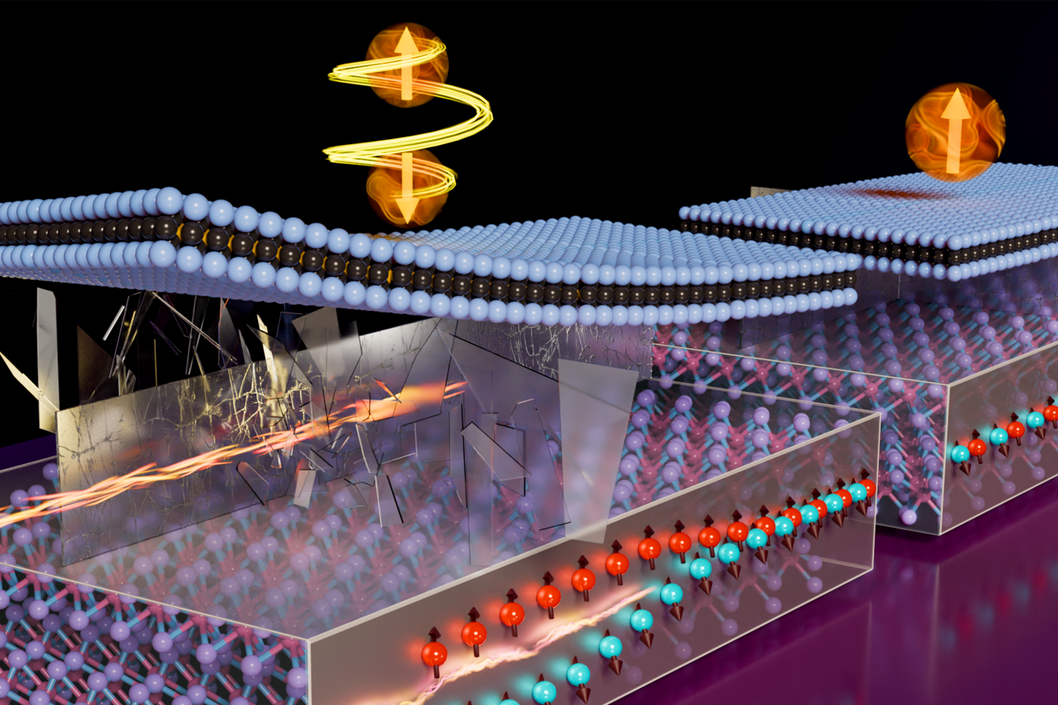
MIT physicists and colleagues have created a five-lane superhighway for electrons that could allow ultra-efficient electronics and more. 

The work, reported in the May 10 issue of Science, is one of several important discoveries by the same team over the past year involving a material that is a unique form of graphene.

“This discovery has direct implications for low-power electronic devices because no energy is lost during the propagation of electrons, which is not the case in regular materials where the electrons are scattered,” says Long Ju, an assistant professor in the Department of Physics and corresponding author of the Science paper.

The phenomenon is akin to cars traveling down an open turnpike as opposed to those moving through neighborhoods. The neighborhood cars can be stopped or slowed by other drivers making abrupt stops or U-turns that disrupt an otherwise smooth commute.

A new material

The material behind this work, known as rhombohedral pentalayer graphene, was discovered two years ago by physicists led by Ju. “We found a goldmine, and every scoop is revealing something new,” says Ju, who is also affiliated with MIT’s Materials Research Laboratory.

In a Nature Nanotechnology paper last October, Ju and colleagues reported the discovery of three important properties arising from rhombohedral graphene. For example, they showed that it could be topological, or allow the unimpeded movement of electrons around the edge of the material but not through the middle. That resulted in a superhighway, but required the application of a large magnetic field some tens of thousands times stronger than the Earth’s magnetic field.

In the current work, the team reports creating the superhighway without any magnetic field.

Tonghang Han, an MIT graduate student in physics, is a co-first author of the paper. “We are not the first to discover this general phenomenon, but we did so in a very different system. And compared to previous systems, ours is simpler and also supports more electron channels.” Explains Ju, “other materials can only support one lane of traffic on the edge of the material. We suddenly bumped it up to five.”

Additional co-first authors of the paper who contributed equally to the work are Zhengguang Lu and Yuxuan Yao. Lu is a postdoc in the Materials Research Laboratory. Yao conducted the work as a visiting undergraduate student from Tsinghua University. Other authors are MIT professor of physics Liang Fu; Jixiang Yang and Junseok Seo, both MIT graduate students in physics; Chiho Yoon and Fan Zhang of the University of Texas at Dallas; and Kenji Watanabe and Takashi Taniguchi of the National Institute for Materials Science in Japan.

How it works

Graphite, the primary component of pencil lead, is composed of many layers of graphene, a single layer of carbon atoms arranged in hexagons resembling a honeycomb structure. Rhombohedral graphene is composed of five layers of graphene stacked in a specific overlapping order.

Ju and colleagues isolated rhombohedral graphene thanks to a novel microscope Ju built at MIT in 2021 that can quickly and relatively inexpensively determine a variety of important characteristics of a material at the nanoscale. Pentalayer rhombohedral stacked graphene is only a few billionths of a meter thick.

In the current work, the team tinkered with the original system, adding a layer of tungsten disulfide (WS2). “The interaction between the WSand the pentalayer rhombohedral graphene resulted in this five-lane superhighway that operates at zero magnetic field,” says Ju.

Comparison to superconductivity

The phenomenon that the Ju group discovered in rhombohedral graphene that allows electrons to travel with no resistance at zero magnetic field is known as the quantum anomalous Hall effect. Most people are more familiar with superconductivity, a completely different phenomenon that does the same thing but happens in very different materials.

Ju notes that although superconductors were discovered in the 1910s, it took some 100 years of research to coax the system to work at the higher temperatures necessary for applications. “And the world record is still well below room temperature,” he notes.

Similarly, the rhombohedral graphene superhighway currently operates at about 2 kelvins, or -456 degrees Fahrenheit. “It will take a lot of effort to elevate the temperature, but as physicists, our job is to provide the insight; a different way for realizing this [phenomenon],” Ju says.

Very exciting

The discoveries involving rhombohedral graphene came as a result of painstaking research that wasn’t guaranteed to work. “We tried many recipes over many months,” says Han, “so it was very exciting when we cooled the system to a very low temperature and [a five-lane superhighway operating at zero magnetic field] just popped out.”

Says Ju, “it’s very exciting to be the first to discover a phenomenon in a new system, especially in a material that we uncovered.”

This work was supported by a Sloan Fellowship; the U.S. National Science Foundation; the U.S. Office of the Under Secretary of Defense for Research and Engineering; the Japan Society for the Promotion of Science KAKENHI; and the World Premier International Research Initiative of Japan.

© Image: Sampson Wilcox/Research Laboratory of Electronics

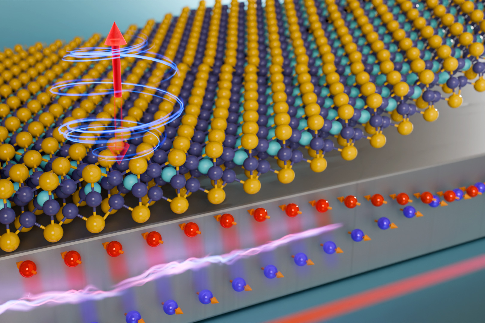
Artist’s rendition of a newly discovered superhighway for electrons that can occur in rhombohedral graphene. “We found a goldmine, and every scoop is revealing something new,” says MIT Assistant Professor Long Ju.

Using art and science to depict the MIT family from 1861 to the present

In MIT.nano’s laboratories, researchers use silicon wafers as the platform to shape transformative technologies such as quantum circuitry, microfluidic devices, or energy-harvesting structures. But these substrates can also serve as a canvas for an artist, as MIT Professor W. Craig Carter demonstrates in the latest One.MIT mosaic.

The One.MIT project celebrates the people of MIT by using the tools of MIT.nano to etch their collective names, arranged as a mosaic by Carter, into a silicon wafer just 8 inches in diameter. The latest edition of One.MIT — including 339,537 names of students, faculty, staff, and alumni associated with MIT from 1861 to September 2023 — is now on display in the ground-floor galleries at MIT.nano in the Lisa T. Su Building (Building 12).

“A spirit of innovation and a relentless drive to solve big problems have permeated the campus in every decade of our history. This passion for discovery, learning, and invention is the thread connecting MIT’s 21st-century family to our 19th-century beginnings and all the years in between,” says Vladimir Bulović, director of MIT.nano and the Fariborz Maseeh Chair in Emerging Technology. “One.MIT celebrates the MIT ethos and reminds us that no matter when we came to MIT, whatever our roles, we all leave a mark on this remarkable community.”

A team of students, faculty, staff, and alumni inscribed the design on the wafer inside the MIT.nano cleanrooms. Because the names are too small to be seen with the naked eye — they measure only microns high on the wafer — the One.MIT website allows anyone to look up a name and find its location in the mosaic.

Finding inspiration in the archives

The first two One.MIT art pieces, created in 2018 and 2020, were inscribed in silicon wafers 6 inches in diameter, slightly smaller than the latest art piece, which benefited from the newest MIT.nano tools that can fabricate 8-inch wafers. The first designs form well-known, historic MIT images: the Great Dome (2018) and the MIT seal (2020).

Carter, who is the Toyota Professor of Materials Processing and professor of materials science and engineering, created the designs and algorithms for each version of One.MIT. He started a search last summer for inspiration for the 2024 design. “The image needed to be iconic of MIT,” says Carter, “and also work within the constraints of a large-scale mosaic.”

Carter ultimately found the solution within the Institute Archives, in the form of a lithograph used on the cover of a program for the 1916 MIT rededication ceremony that celebrated the Institute’s move from Boston to Cambridge on its 50th anniversary.

Incorporating MIT nerdiness

Carter began by creating a black-and-white image, redrawing the lithograph’s architectural features and character elements. He recreated the kerns (spaces) and the fonts of the letters as algorithmic geometric objects.

The color gradient of the sky behind the dome presented a challenge because only two shades were available. To tackle this issue and impart texture, Carter created a Hilbert curve — a hierarchical, continuous curve made by replacing an element with a combination of four elements. Each of these four elements are replaced by another four elements, and so on. The resulting object is like a fractal — the curve changes shape as it goes from top to bottom, with 90-degree turns throughout.

“This was an opportunity to add a fun and ‘nerdy’ element — fitting for MIT,” says Carter.

To achieve both the gradient and the round wafer shape, Carter morphed the square Hilbert curve (consisting of 90-degree angles) into a disk shape using Schwarz-Christoffel mapping, a type of conformal mapping that can be used to solve problems in many different domains.

“Conformal maps are lovely convergences of physics and engineering with mathematics and geometry,” says Carter.

Because the conformal mapping is smooth and also preserves the angles, the square’s corners produce four singular points on the circle where the Hilbert curve’s line segments shrink to a point. The location of the four points in the upper part of the circle “squeezes” the curve and creates the gradient (and the texture of the illustration) — dense-to-sparse from top-to-bottom.

The final mosaic is made up of 6,476,403 characters, and Carter needed to use font and kern types that would fill as much of the wafer’s surface as possible without having names break up and wrap around to the next line. Carter’s algorithm alleviated this problem, at least somewhat, by searching for names that slotted into remaining spaces at the end of each row. The algorithm also performed an optimization over many different choices for the random order of the names. 

Finding — and wrangling — hundreds of thousands of names

In addition to the art and algorithms, the foundation of One.MIT is the extensive collection of names spanning more than 160 years of MIT. The names reflect students, alumni, faculty, and staff — the wide variety of individuals who have always formed the MIT community.

Annie Wang, research scientist and special projects coordinator for MIT.nano, again played an instrumental role in collecting the names for the project, just as she had for the 2018 and 2020 versions. Despite her experience, collating the names to construct the newest edition still presented several challenges, given the variety of input sources to the dataset and the need to format names in a consistent manner.

“Both databases and OCR-scanned text can be messy,” says Wang, referring to the electronic databases and old paper directories from which names were sourced. “And cleaning them up is a lot of work.”

Many names were listed in multiple places, sometimes spelled or formatted differently across sources. There were very short first and last names, very long first and last names — and also a portion of names in which more than one person had nearly identical names. And some groups are simply hard to find in the records. “One thing I wish we had,” comments Wang, “is a list of long-term volunteers at MIT who contribute so much but aren’t reflected in the main directories.”

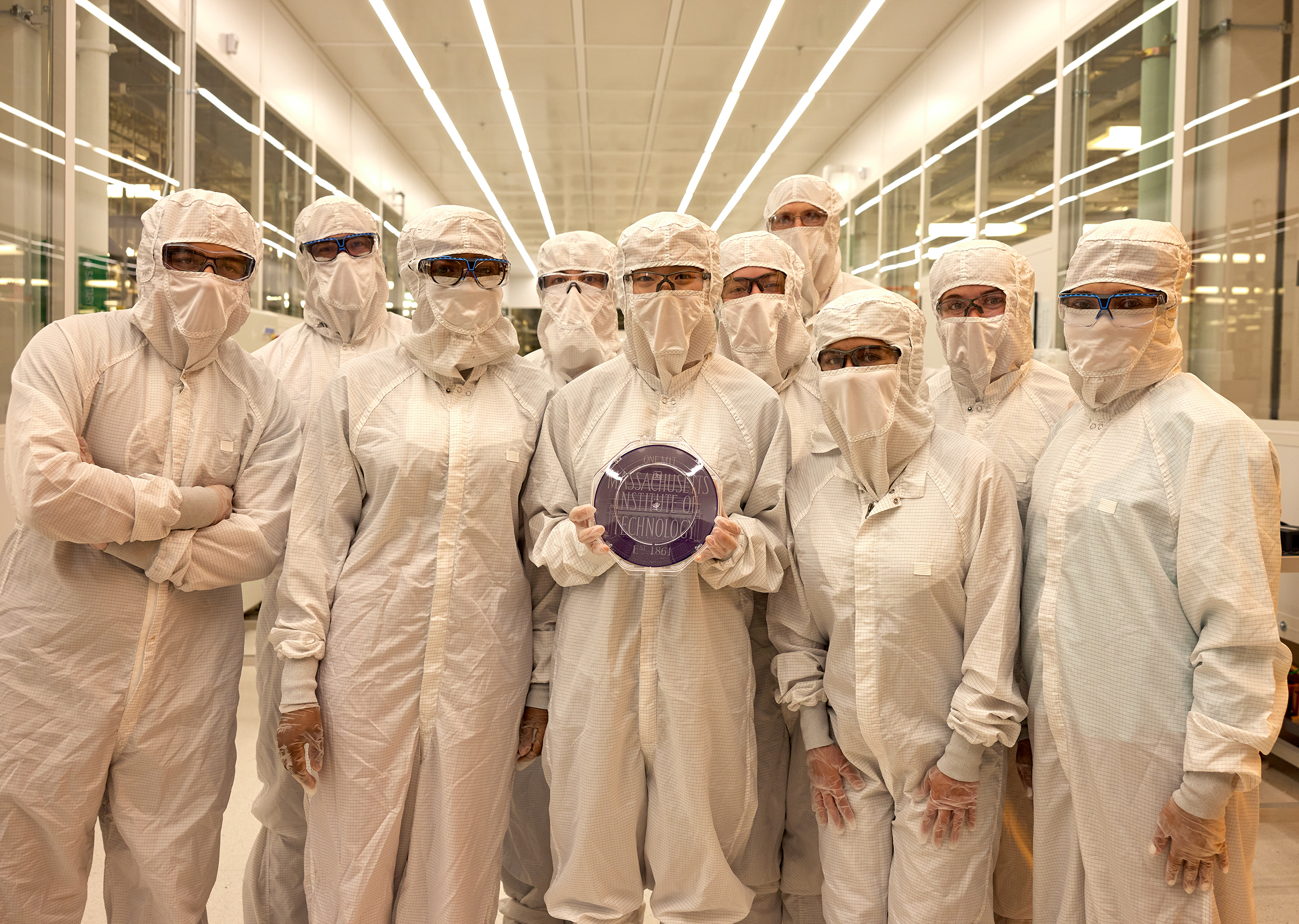
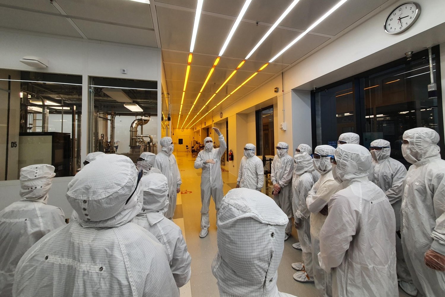
Once the design was completed, Carter and Wang handed off a CAD file to Jorg Scholvin, associate director of fabrication at MIT.nano. Scholvin assembled a team that reflected One.MIT — students, faculty, staff, and alumni — and worked with them to fabricate the wafer inside MIT.nano’s cleanroom. The fab team included Carter; undergraduate students Akorfa Dagadu, Sean Luk, Emilia K. Szczepaniak, Amber Velez, and twin brothers Juan Antonio Luera and Juan Angel Luera; MIT Sloan School of Management EMBA student Patricia LaBorda; staff member Kevin Verrier of MIT Facilities; and alumnae Madeline Hickman '11 and Eboney Hearn '01, who is also the executive director of MIT Introduction to Technology, Engineering and Science (MITES).

© Photo: Ken Richardson

A team of MIT students, faculty, staff, and alumni fabricated a new One.MIT wafer inside MIT.nano’s cleanroom. The fab team included undergraduate students Akorfa Dagadu, Sean Luk, Emilia K Szczepaniak, Amber Velez, and twin brothers Juan Antonio Luera and Juan Angel Luera; Sloan Executive MBA student Patricia LaBorda; staff member Kevin Verrier of MIT Facilities; and alumnae Madeline Hickman '11 and Eboney Hearn '01, who is also the executive director of MIT Introduction to Technology, Engineering and Science (MITES).
  • ✇MIT News - Nanoscience and nanotechnology | MIT.nano
  • Turning up the heat on next-generation semiconductorsAdam Zewe | MIT News
    The scorching surface of Venus, where temperatures can climb to 480 degrees Celsius (hot enough to melt lead), is an inhospitable place for humans and machines alike. One reason scientists have not yet been able to send a rover to the planet’s surface is because silicon-based electronics can’t operate in such extreme temperatures for an extended period of time.For high-temperature applications like Venus exploration, researchers have recently turned to gallium nitride, a unique material that can
     

Turning up the heat on next-generation semiconductors

The scorching surface of Venus, where temperatures can climb to 480 degrees Celsius (hot enough to melt lead), is an inhospitable place for humans and machines alike. One reason scientists have not yet been able to send a rover to the planet’s surface is because silicon-based electronics can’t operate in such extreme temperatures for an extended period of time.

For high-temperature applications like Venus exploration, researchers have recently turned to gallium nitride, a unique material that can withstand temperatures of 500 degrees or more.

The material is already used in some terrestrial electronics, like phone chargers and cell phone towers, but scientists don’t have a good grasp of how gallium nitride devices would behave at temperatures beyond 300 degrees, which is the operational limit of conventional silicon electronics.

In a new paper published in Applied Physics Letterswhich is part of a multiyear research effort, a team of scientists from MIT and elsewhere sought to answer key questions about the material’s properties and performance at extremely high temperatures.  

They studied the impact of temperature on the ohmic contacts in a gallium nitride device. Ohmic contacts are key components that connect a semiconductor device with the outside world.

The researchers found that extreme temperatures didn’t cause significant degradation to the gallium nitride material or contacts. They were surprised to see that the contacts remained structurally intact even when held at 500 degrees Celsius for 48 hours.

Understanding how contacts perform at extreme temperatures is an important step toward the group’s next goal of developing high-performance transistors that could operate on the surface of Venus. Such transistors could also be used on Earth in electronics for applications like extracting geothermal energy or monitoring the inside of jet engines.

“Transistors are the heart of most modern electronics, but we didn’t want to jump straight to making a gallium nitride transistor because so much could go wrong. We first wanted to make sure the material and contacts could survive, and figure out how much they change as you increase the temperature. We’ll design our transistor from these basic material building blocks,” says John Niroula, an electrical engineering and computer science (EECS) graduate student and lead author of the paper.

His co-authors include Qingyun Xie PhD ’24; Mengyang Yuan PhD ’22; EECS graduate students Patrick K. Darmawi-Iskandar and Pradyot Yadav; Gillian K. Micale, a graduate student in the Department of Materials Science and Engineering; senior author Tomás Palacios, the Clarence J. LeBel Professor of EECS, director of the Microsystems Technology Laboratories, and a member of the Research Laboratory of Electronics; as well as collaborators Nitul S. Rajput of the Technology Innovation Institute of the United Arab Emirates; Siddharth Rajan of Ohio State University; Yuji Zhao of Rice University; and Nadim Chowdhury of Bangladesh University of Engineering and Technology.

Turning up the heat

While gallium nitride has recently attracted much attention, the material is still decades behind silicon when it comes to scientists’ understanding of how its properties change under different conditions. One such property is resistance, the flow of electrical current through a material.

A device’s overall resistance is inversely proportional to its size. But devices like semiconductors have contacts that connect them to other electronics. Contact resistance, which is caused by these electrical connections, remains fixed no matter the size of the device. Too much contact resistance can lead to higher power dissipation and slower operating frequencies for electronic circuits.

“Especially when you go to smaller dimensions, a device’s performance often ends up being limited by contact resistance. People have a relatively good understanding of contact resistance at room temperature, but no one has really studied what happens when you go all the way up to 500 degrees,” Niroula says.

For their study, the researchers used facilities at MIT.nano to build gallium nitride devices known as transfer length method structures, which are composed of a series of resistors. These devices enable them to measure the resistance of both the material and the contacts.

They added ohmic contacts to these devices using the two most common methods. The first involves depositing metal onto gallium nitride and heating it to 825 degrees Celsius for about 30 seconds, a process called annealing.

The second method involves removing chunks of gallium nitride and using a high-temperature technology to regrow highly doped gallium nitride in its place, a process led by Rajan and his team at Ohio State. The highly doped material contains extra electrons that can contribute to current conduction.

“The regrowth method typically leads to lower contact resistance at room temperature, but we wanted to see if these methods still work well at high temperatures,” Niroula says.

A comprehensive approach

They tested devices in two ways. Their collaborators at Rice University, led by Zhao, conducted short-term tests by placing devices on a hot chuck that reached 500 degrees Celsius and taking immediate resistance measurements.

At MIT, they conducted longer-term experiments by placing devices into a specialized furnace the group previously developed. They left devices inside for up to 72 hours to measure how resistance changes as a function of temperature and time.

Microscopy experts at MIT.nano (Aubrey N. Penn) and the Technology Innovation Institute (Nitul S. Rajput) used state-of-the-art transmission electron microscopes to see how such high temperatures affect gallium nitride and the ohmic contacts at the atomic level.

“We went in thinking the contacts or the gallium nitride material itself would degrade significantly, but we found the opposite. Contacts made with both methods seemed to be remarkably stable,” says Niroula.

While it is difficult to measure resistance at such high temperatures, their results indicate that contact resistance seems to remain constant even at temperatures of 500 degrees, for around 48 hours. And just like at room temperature, the regrowth process led to better performance.

The material did start to degrade after being in the furnace for 48 hours, but the researchers are already working to boost long-term performance. One strategy involves adding protective insulators to keep the material from being directly exposed to the high-temperature environment.

Moving forward, the researchers plan to use what they learned in these experiments to develop high-temperature gallium nitride transistors.

“In our group, we focus on innovative, device-level research to advance the frontiers of microelectronics, while adopting a systematic approach across the hierarchy, from the material level to the circuit level. Here, we have gone all the way down to the material level to understand things in depth. In other words, we have translated device-level advancements to circuit-level impact for high-temperature electronics, through design, modeling and complex fabrication. We are also immensely fortunate to have forged close partnerships with our longtime collaborators in this journey,” Xie says.

This work was funded, in part, by the U.S. Air Force Office of Scientific Research, Lockheed Martin Corporation, the Semiconductor Research Corporation through the U.S. Defense Advanced Research Projects Agency, the U.S. Department of Energy, Intel Corporation, and the Bangladesh University of Engineering and Technology.

Fabrication and microscopy were conducted at MIT.nano, the Semiconductor Epitaxy and Analysis Laboratory at Ohio State University, the Center for Advanced Materials Characterization at the University of Oregon, and the Technology Innovation Institute of the United Arab Emirates.

© Image: MIT News; iStock

Researchers studied how temperatures up to 500 degrees Celsius would affect electronic devices made from gallium nitride, a key step in their multiyear research effort to develop electronics that can operate in extremely hot environments, like the surface of Venus.

Study: Under extreme impacts, metals get stronger when heated

Metals get softer when they are heated, which is how blacksmiths can form iron into complex shapes by heating it red hot. And anyone who compares a copper wire with a steel coat hanger will quickly discern that copper is much more pliable than steel.

But scientists at MIT have discovered that when metal is struck by an object moving at a super high velocity, the opposite happens: The hotter the metal, the stronger it is. Under those conditions, which put extreme stress on the metal, copper can actually be just as strong as steel. The new discovery could lead to new approaches to designing materials for extreme environments, such as shields that protect spacecraft or hypersonic aircraft, or equipment for high-speed manufacturing processes.

The findings are described in a paper appearing today in the journal Nature, by Ian Dowding, an MIT graduate student, and Christopher Schuh, former head of MIT’s Department of Materials Science and Engineering, now dean of engineering at Northwestern University and visiting professor at MIT.

The new finding, the authors write, “is counterintuitive and at odds with decades of studies in less extreme conditions.” The unexpected results could affect a variety of applications because the extreme velocities involved in these impacts occur routinely in meteorite impacts on spacecraft in orbit and in high-speed machining operations used in manufacturing, sandblasting, and some additive manufacturing (3D printing) processes.

The experiments the researchers used to find this effect involved shooting tiny particles of sapphire, just millionths of a meter across, at flat sheets of metal. Propelled by laser beams, the particles reached high velocities, on the order of a few hundred meters per second. While other researchers have occasionally done experiments at similarly high velocities, they have tended to use larger impactors, at the scale of centimeters or larger. Because these larger impacts were dominated by effects of the shock of the impact, there was no way to separate out the mechanical and thermal effects.

The tiny particles in the new study don’t create a significant pressure wave when they hit the target. But it has taken a decade of research at MIT to develop methods of propelling such microscopic particles at such high velocities. “We’ve taken advantage of that,” Schuh says, along with other new techniques for observing the high-speed impact itself.

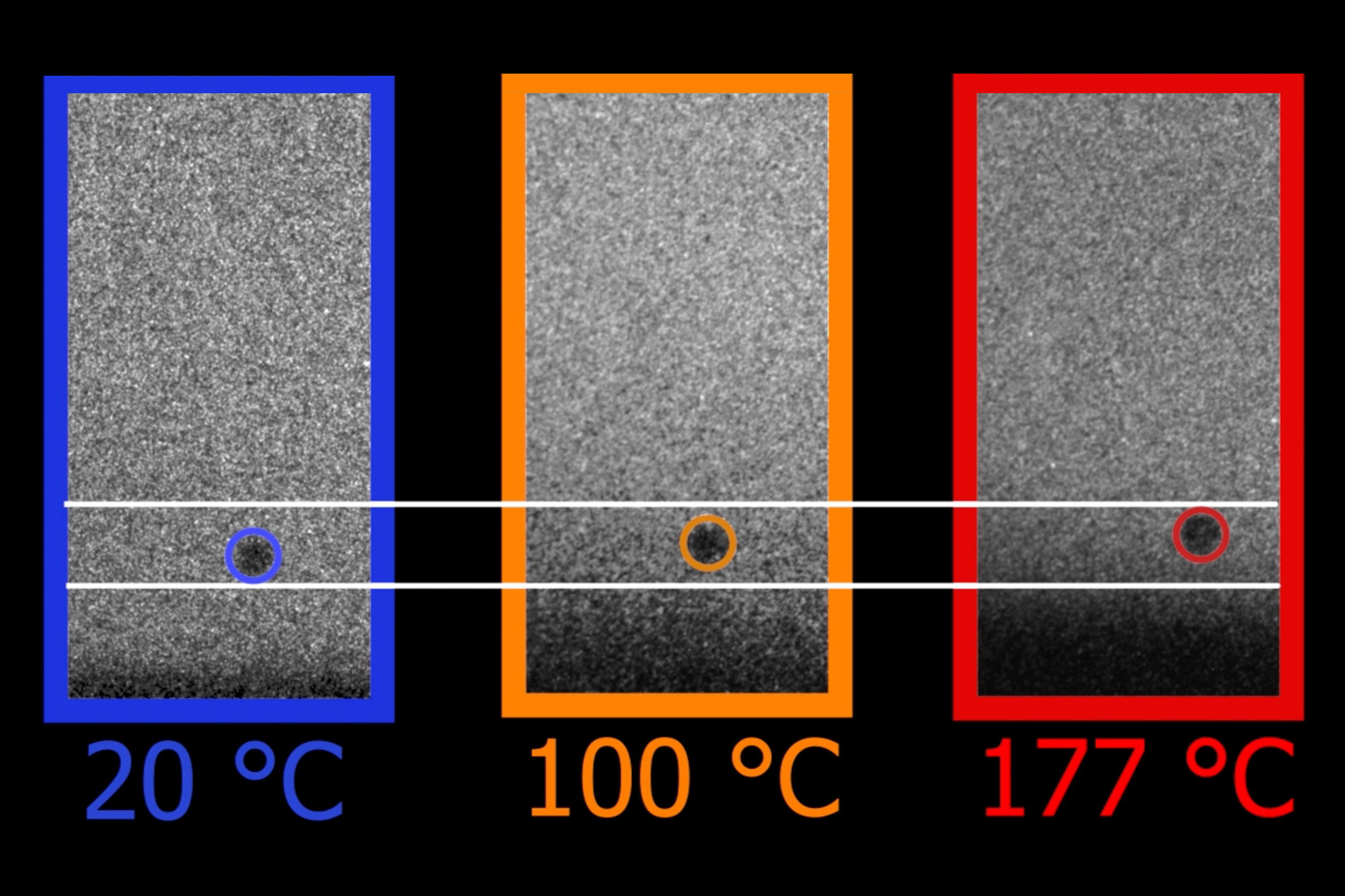
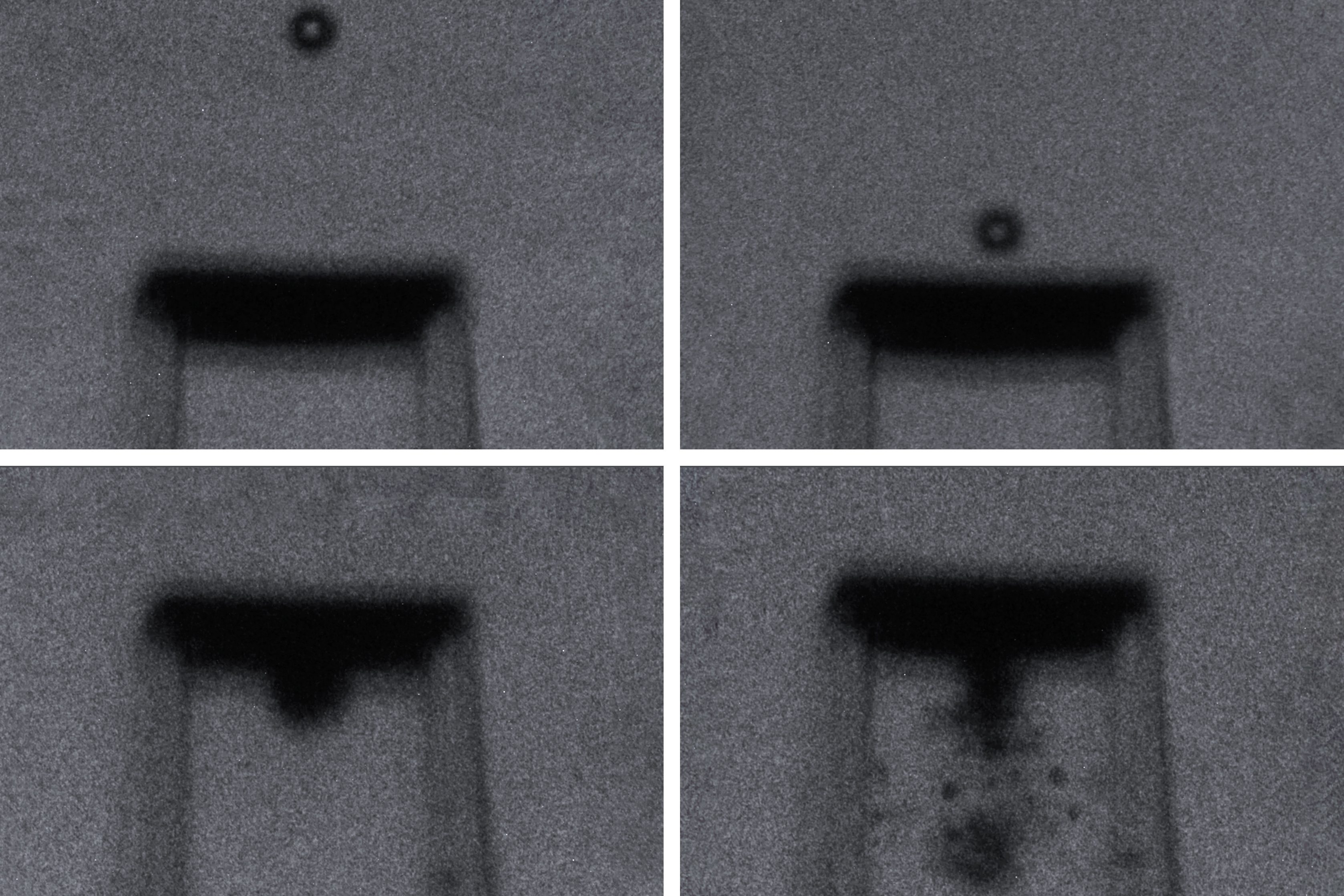
The team used extremely high-speed cameras “to watch the particles as they come in and as they fly away,” he says. As the particles bounce off the surface, the difference between the incoming and outgoing velocities “tells you how much energy was deposited” into the target, which is an indicator of the surface strength.

Three photos show a particle bouncing off of a surface. The particle bounces higher when the temperature is increased. These three images are labeled “20 °C, 100 °C, and 177 °C.” A series of 16 monochrome photos show a tiny particle bouncing on a surface.

The tiny particles they used were made of alumina, or sapphire, and are “very hard,” Dowding says. At 10 to 20 microns (millionths of a meter) across, these are between one-tenth and one-fifth of the thickness of a human hair. When the launchpad behind those particles is hit by a laser beam, part of the material vaporizes, creating a jet of vapor that propels the particle in the opposite direction.

The researchers shot the particles at samples of copper, titanium, and gold, and they expect their results should apply to other metals as well. They say their data provide the first direct experimental evidence for this anomalous thermal effect of increased strength with greater heat, although hints of such an effect had been reported before.

The surprising effect appears to result from the way the orderly arrays of atoms that make up the crystalline structure of metals move under different conditions, according to the researchers’ analysis. They show that there are three separate effects governing how metal deforms under stress, and while two of these follow the predicted trajectory of increasing deformation at higher temperatures, it is the third effect, called drag strengthening, that reverses its effect when the deformation rate crosses a certain threshold.

Beyond this crossover point, the higher temperature increases the activity of phonons — waves of sound or heat — within the material, and these phonons interact with dislocations in the crystalline lattice in a way that limits their ability to slip and deform. The effect increases with increased impact speed and temperature, Dowding says, so that “the faster you go, the less the dislocations are able to respond.”

Of course, at some point the increased temperature will begin to melt the metal, and at that point the effect will reverse again and lead to softening. “There will be a limit” to this strengthening effect, Dowding says, “but we don’t know what it is.”

The findings could lead to different choices of materials when designing devices that may encounter such extreme stresses, Schuh says. For example, metals that may ordinarily be much weaker, but that are less expensive or easier to process, might be useful in situations where nobody would have thought to use them before.

The extreme conditions the researchers studied are not confined to spacecraft or extreme manufacturing methods. “If you are flying a helicopter in a sandstorm, a lot of these sand particles will reach high velocities as they hit the blades,” Dowding says, and under desert conditions they may reach the high temperatures where these hardening effects kick in.

The techniques the researchers used to uncover this phenomenon could be applied to a variety of other materials and situations, including other metals and alloys. Designing materials to be used in extreme conditions by simply extrapolating from known properties at less extreme conditions could lead to seriously mistaken expectations about how materials will behave under extreme stresses, they say.

The research was supported by the U.S. Department of Energy.

© Image: Courtesy of the researchers

MIT scientists discovered that when metals are deformed at an extreme rate by an object moving at high velocities, hotter temperatures make the metal stronger, not weaker. Here, 3 particles are hitting a metallic surface at about the same velocity. As the initial temperature of the metal is increased, the rebound is faster, and the particle bounces higher because the metal becomes harder not softer, too.

Jeong Min Park earns 2024 Schmidt Science Fellowship

Physics graduate student Jeong Min (Jane) Park is among the 32 exceptional early-career scientists worldwide chosen to receive the prestigious 2024 Schmidt Science Fellows award.  

As a 2024 Schmidt Science Fellow, Park’s postdoctoral work will seek to directly detect phases that could host new particles by employing an instrument that can visualize subatomic-scale phenomena.  

With her advisor, Pablo Jarillo-Herrero, the Cecil and Ida Green Professor of Physics, Park’s research at MIT focuses on discovering novel quantum phases of matter.

“When there are many electrons in a material, their interactions can lead to collective behaviors that are not expected from individual particles, known as emergent phenomena,” explains Park. “One example is superconductivity, where interacting electrons combine together as a pair at low temperatures to conduct electricity without energy loss.”

During her PhD studies, she has investigated novel types of superconductivity by designing new materials with targeted interactions and topology. In particular, she used graphene, atomically thin two-dimensional layers of graphite, the same material as pencil lead, and turned it into a “magic” material. This so-called magic-angle twisted trilayer graphene provided an extraordinarily strong form of superconductivity that is robust under high magnetic fields. Later, she found a whole “magic family” of these materials, elucidating the key mechanisms behind superconductivity and interaction-driven phenomena. These results have provided a new platform to study emergent phenomena in two dimensions, which can lead to innovations in electronics and quantum technology.

Park says she is looking forward to her postdoctoral studies with Princeton University physics professor Ali Yazdani's lab.

“I’m excited about the idea of discovering and studying new quantum phenomena that could further the understanding of fundamental physics,” says Park. “Having explored interaction-driven phenomena through the design of new materials, I’m now aiming to broaden my perspective and expertise to address a different kind of question, by combining my background in material design with the sophisticated local-scale measurements that I will adopt during my postdoc.”

She explains that elementary particles are classified as either bosons or fermions, with contrasting behaviors upon interchanging two identical particles, referred to as exchange statistics; bosons remain unchanged, while fermions acquire a minus sign in their quantum wavefunction.

Theories predict the existence of fundamentally different particles known as non-abelian anyons, whose wavefunctions braid upon particle exchange. Such a braiding process can be used to encode and store information, potentially opening the door to fault-tolerant quantum computing in the future.

Since 2018, this prestigious postdoctoral program has sought to break down silos among scientific fields to solve the world’s biggest challenges and support future leaders in STEM.

Schmidt Science Fellows, an initiative of Schmidt Sciences, delivered in partnership with the Rhodes Trust, identifies, develops, and amplifies the next generation of science leaders, by building a community of scientists and supporters of interdisciplinary science and leveraging this network to drive sector-wide change. The 2024 fellows consist of 17 nationalities across North America, Europe, and Asia.   

Nominated candidates undergo a rigorous selection process that includes a paper-based academic review with panels of experts in their home disciplines and final interviews with panels, including senior representatives from across many scientific disciplines and different business sectors.  

© Photo courtesy of the Department of Physics

Physics graduate student Jeong Min (Jane) Park is among the 32 exceptional early-career scientists worldwide chosen to receive the prestigious 2024 Schmidt Science Fellows award.
  • ✇MIT News - Nanoscience and nanotechnology | MIT.nano
  • John Joannopoulos receives 2024-2025 Killian AwardJennifer Chu | MIT News
    John Joannopoulos, an innovator and mentor in the fields of theoretical condensed matter physics and nanophotonics, has been named the recipient of the 2024-2025 James R. Killian Jr. Faculty Achievement Award.Joannopoulos is the Francis Wright Davis Professor of Physics and director of MIT’s Institute for Soldier Nanotechnologies. He has been a member of the MIT faculty for 50 years.“Professor Joannopoulos’s profound and lasting impact on the field of theoretical condensed matter physics finds i
     

John Joannopoulos receives 2024-2025 Killian Award

John Joannopoulos, an innovator and mentor in the fields of theoretical condensed matter physics and nanophotonics, has been named the recipient of the 2024-2025 James R. Killian Jr. Faculty Achievement Award.

Joannopoulos is the Francis Wright Davis Professor of Physics and director of MIT’s Institute for Soldier Nanotechnologies. He has been a member of the MIT faculty for 50 years.

“Professor Joannopoulos’s profound and lasting impact on the field of theoretical condensed matter physics finds its roots in his pioneering work in harnessing ab initio physics to elucidate the behavior of materials at the atomic level,” states the award citation, which was announced at today’s faculty meeting by Roger White, chair of the Killian Award Selection Committee and professor of philosophy at MIT. “His seminal research in the development of photonic crystals has revolutionized understanding of light-matter interactions, laying the groundwork for transformative advancements in diverse fields ranging from telecommunications to biomedical engineering.”

The award also honors Joannopoulos’ service as a “legendary mentor to generations of students, inspiring them to achieve excellence in science while at the same time facilitating the practical benefit to society through entrepreneurship.”

The Killian Award was established in 1971 to recognize outstanding professional contributions by MIT faculty members. It is the highest honor that the faculty can give to one of its members.

“I have to tell you, it was a complete and utter surprise,” Joannopoulos told MIT News shortly after he received word of the award. “I didn’t expect it at all, and was extremely flattered, honored, and moved by it, frankly.”

Joannopoulous has spent his entire professional career at MIT. He came to the Institute in 1974, directly after receiving his PhD in physics at the University of California at Berkeley, where he also earned his bachelor’s degree. Starting out as an assistant professor in MIT’s Department of Physics, he quickly set up a research program focused on theoretical condensed matter physics.

Over the first half of his MIT career, Joannopoulos worked to elucidate the fundamental nature of the electronic, vibrational, and optical structure of crystalline and amorphous bulk solids, their surfaces, interfaces, and defects. He and his students developed numerous theoretical methods to enable tractable and accurate calculations of these complex systems.

In the 1990s, his work with microscopic material systems expanded to a new class of materials, called photonic crystals — materials that could be engineered at the micro- and nanoscale to manipulate light in ways that impart surprising and exotic optical qualities to the material as a whole.

“I saw that you could create photonic crystals with defects that can affect the properties of photons, in much the same way that defects in a semiconductor affect the properties of electrons,” Joannopoulos says. “So I started working in this area to try and explore what anomalous light phenomena can we discover using this approach?”

Among his various breakthroughs in the field was the realization of a “perfect dielectric mirror” — a multilayered optical device that reflects light from all angles as normal metallic mirrors do, and that can also be tuned to reflect and trap light at specific frequencies. He and his colleagues saw potential for the mirror to be made into a hollow fiber that could serve as a highly effective optical conduit, for use in a wide range of applications. To further advance the technology, he and his colleagues launched a startup, which has since developed the technology into a flexible, fiber-optic “surgical scalpel.”

Throughout his career, Joannopoulos has helped to launch numerous startups and photonics-based technologies.

“His ability to bridge the gap between academia and industry has not only advanced scientific knowledge but also led to the creation of dozens of new companies, thousands of jobs, and groundbreaking products that continue to benefit society to this day,” the award citation states.

In 2006, Joannopoulos accepted the position as director of MIT’s Institute for Soldier Nanotechnologies (ISN), a collaboration between MIT researchers, industry partners, and military defense experts, who seek innovations to protect and enhance soldiers’ survivability in the field. In his role as ISN head, Joannopoulos has worked across MIT, making connections and supporting new projects with researchers specializing in fields far from his own.

“I get a chance to explore and learn fascinating new things,” says Joannopoulos, who is currently overseeing projects related to hyperspectral imaging, smart and responsive fabrics, and nanodrug delivery. “I love that aspect of really getting to understand what people in other fields are doing. And they’re doing great work across many, many different fields.”

Throughout his career at MIT, Joannopoulos has been especially inspired and motivated by his students, many of whom have gone on to found companies, lead top academic and research institutions, and make significant contributions to their respective fields, including one student who was awarded the Nobel Prize in Physics in 1998.

“One’s proudest moments are the successes of one’s students, and in that regard, I’ve been extremely lucky to have had truly exceptional students over the years,” Joannopolous says.

His many contributions to academia and industry have earned Joannopoulos numerous honors and awards, including his election to both the National Academy of Sciences and the American Academy of Arts and Sciences. He is also a fellow of both the American Physical Society and the American Association for the Advancement of Science.

“The Selection Committee is delighted to have this opportunity to honor Professor John Joannopoulos: a visionary scientist, a beloved mentor, a great believer in the goodness of people, and a leader whose contributions to MIT and the broader scientific community are immeasurable,” the award citation concludes.

© Photo: Jose-Luis Olivares, MIT

Scientists develop an affordable sensor for lead contamination

Engineers at MIT, Nanyang Technological University, and several companies have developed a compact and inexpensive technology for detecting and measuring lead concentrations in water, potentially enabling a significant advance in tackling this persistent global health issue.

The World Health Organization estimates that 240 million people worldwide are exposed to drinking water that contains unsafe amounts of toxic lead, which can affect brain development in children, cause birth defects, and produce a variety of neurological, cardiac, and other damaging effects. In the United States alone, an estimated 10 million households still get drinking water delivered through lead pipes.

“It’s an unaddressed public health crisis that leads to over 1 million deaths annually,” says Jia Xu Brian Sia, an MIT postdoc and the senior author of the paper describing the new technology.

But testing for lead in water requires expensive, cumbersome equipment and typically requires days to get results. Or, it uses simple test strips that simply reveal a yes-or-no answer about the presence of lead but no information about its concentration. Current EPA regulations require drinking water to contain no more that 15 parts per billion of lead, a concentration so low it is difficult to detect.

The new system, which could be ready for commercial deployment within two or three years, could detect lead concentrations as low as 1 part per billion, with high accuracy, using a simple chip-based detector housed in a handheld device. The technology gives nearly instant quantitative measurements and requires just a droplet of water.

The findings are described in a paper appearing today in the journal Nature Communications, by Sia, MIT graduate student and lead author Luigi Ranno, Professor Juejun Hu, and 12 others at MIT and other institutions in academia and industry.

The team set out to find a simple detection method based on the use of photonic chips, which use light to perform measurements. The challenging part was finding a way to attach to the photonic chip surface certain ring-shaped molecules known as crown ethers, which can capture specific ions such as lead. After years of effort, they were able to achieve that attachment via a chemical process known as Fischer esterification. “That is one of the essential breakthroughs we have made in this technology,” Sia says.

In testing the new chip, the researchers showed that it can detect lead in water at concentrations as low as one part per billion. At much higher concentrations, which may be relevant for testing environmental contamination such as mine tailings, the accuracy is within 4 percent.

The device works in water with varying levels of acidity, ranging from pH values of 6 to 8, “which covers most environmental samples,” Sia says. They have tested the device with seawater as well as tap water, and verified the accuracy of the measurements.

In order to achieve such levels of accuracy, current testing requires a device called an inductive coupled plasma mass spectrometer. “These setups can be big and expensive,” Sia says. The sample processing can take days and requires experienced technical personnel.

While the new chip system they developed is “the core part of the innovation,” Ranno says, further work will be needed to develop this into an integrated, handheld device for practical use. “For making an actual product, you would need to package it into a usable form factor,” he explains. This would involve having a small chip-based laser coupled to the photonic chip. “It’s a matter of mechanical design, some optical design, some chemistry, and figuring out the supply chain,” he says. While that takes time, he says, the underlying concepts are straightforward.

The system can be adapted to detect other similar contaminants in water, including cadmium, copper, lithium, barium, cesium, and radium, Ranno says. The device could be used with simple cartridges that can be swapped out to detect different elements, each using slightly different crown ethers that can bind to a specific ion.

“There’s this problem that people don’t measure their water enough, especially in the developing countries,” Ranno says. “And that’s because they need to collect the water, prepare the sample, and bring it to these huge instruments that are extremely expensive.” Instead, “having this handheld device, something compact that even untrained personnel can just bring to the source for on-site monitoring, at low costs,” could make regular, ongoing widespread testing feasible.

Hu, who is the John F. Elliott Professor of Materials Science and Engineering, says, “I’m hoping this will be quickly implemented, so we can benefit human society. This is a good example of a technology coming from a lab innovation where it may actually make a very tangible impact on society, which is of course very fulfilling.”

“If this study can be extended to simultaneous detection of multiple metal elements, especially the presently concerning radioactive elements, its potential would be immense,” says Hou Wang, an associate professor of environmental science and engineering at Hunan University in China, who was not associated with this work.

Wang adds, “This research has engineered a sensor capable of instantaneously detecting lead concentration in water. This can be utilized in real-time to monitor the lead pollution concentration in wastewater discharged from industries such as battery manufacturing and lead smelting, facilitating the establishment of industrial wastewater monitoring systems. I think the innovative aspects and developmental potential of this research are quite commendable.”

Wang Qian, a principal research scientist at A*STAR’s Institute of Materials Research in Singapore, who also was not affiliated with this work, says, “The ability for the pervasive, portable, and quantitative detection of lead has proved to be challenging primarily due to cost concerns. This work demonstrates the potential to do so in a highly integrated form factor and is compatible with large-scale, low-cost manufacturing.”

The team included researchers at MIT, at Nanyang Technological University and Temasek Laboratories in Singapore, at the University of Southampton in the U.K., and at companies Fingate Technologies, in Singapore, and Vulcan Photonics, headquartered in Malaysia. The work used facilities at MIT.nano, the Harvard University Center for Nanoscale Systems, NTU’s Center for Micro- and Nano-Electronics, and the Nanyang Nanofabrication Center.

© Image: Jia Xu Brian Sia

Artist’s impression of the chip surface, showing the on-chip light interferometer used to sense the presence of lead. The lead binding process to the crown ether is shown in the inset.
  • ✇MIT News - Nanoscience and nanotechnology | MIT.nano
  • Seizing solar’s bright futureLeda Zimmerman | MIT Energy Initiative
    Consider the dizzying ascent of solar energy in the United States: In the past decade, solar capacity increased nearly 900 percent, with electricity production eight times greater in 2023 than in 2014. The jump from 2022 to 2023 alone was 51 percent, with a record 32 gigawatts (GW) of solar installations coming online. In the past four years, more solar has been added to the grid than any other form of generation. Installed solar now tops 179 GW, enough to power nearly 33 million homes. The U.S.
     

Seizing solar’s bright future

Consider the dizzying ascent of solar energy in the United States: In the past decade, solar capacity increased nearly 900 percent, with electricity production eight times greater in 2023 than in 2014. The jump from 2022 to 2023 alone was 51 percent, with a record 32 gigawatts (GW) of solar installations coming online. In the past four years, more solar has been added to the grid than any other form of generation. Installed solar now tops 179 GW, enough to power nearly 33 million homes. The U.S. Department of Energy (DOE) is so bullish on the sun that its decarbonization plans envision solar satisfying 45 percent of the nation’s electricity demands by 2050.

But the continued rapid expansion of solar requires advances in technology, notably to improve the efficiency and durability of solar photovoltaic (PV) materials and manufacturing. That’s where Optigon, a three-year-old MIT spinout company, comes in.

“Our goal is to build tools for research and industry that can accelerate the energy transition,” says Dane deQuilettes, the company’s co-founder and chief science officer. “The technology we have developed for solar will enable measurements and analysis of materials as they are being made both in lab and on the manufacturing line, dramatically speeding up the optimization of PV.”

With roots in MIT’s vibrant solar research community, Optigon is poised for a 2024 rollout of technology it believes will drastically pick up the pace of solar power and other clean energy projects.

Beyond silicon

Silicon, the material mainstay of most PV, is limited by the laws of physics in the efficiencies it can achieve converting photons from the sun into electrical energy. Silicon-based solar cells can theoretically reach power conversion levels of just 30 percent, and real-world efficiency levels hover in the low 20s. But beyond the physical limitations of silicon, there is another issue at play for many researchers and the solar industry in the United States and elsewhere: China dominates the silicon PV market, from supply chains to manufacturing.

Scientists are eagerly pursuing alternative materials, either for enhancing silicon’s solar conversion capacity or for replacing silicon altogether.

In the past decade, a family of crystal-structured semiconductors known as perovskites has risen to the fore as a next-generation PV material candidate. Perovskite devices lend themselves to a novel manufacturing process using printing technology that could circumvent the supply chain juggernaut China has built for silicon. Perovskite solar cells can be stacked on each other or layered atop silicon PV, to achieve higher conversion efficiencies. Because perovskite technology is flexible and lightweight, modules can be used on roofs and other structures that cannot support heavier silicon PV, lowering costs and enabling a wider range of building-integrated solar devices.

But these new materials require testing, both during R&D and then on assembly lines, where missing or defective optical, electrical, or dimensional properties in the nano-sized crystal structures can negatively impact the end product.

“The actual measurement and data analysis processes have been really, really slow, because you have to use a bunch of separate tools that are all very manual,” says Optigon co-founder and chief executive officer Anthony Troupe ’21. “We wanted to come up with tools for automating detection of a material’s properties, for determining whether it could make a good or bad solar cell, and then for optimizing it.”

“Our approach packed several non-contact, optical measurements using different types of light sources and detectors into a single system, which together provide a holistic, cross-sectional view of the material,” says Brandon Motes ’21, ME ’22, co-founder and chief technical officer.

“This breakthrough in achieving millisecond timescales for data collection and analysis means we can take research-quality tools and actually put them on a full production system, getting extremely detailed information about products being built at massive, gigawatt scale in real-time,” says Troupe.

This streamlined system takes measurements “in the snap of the fingers, unlike the traditional tools,” says Joseph Berry, director of the US Manufacturing of Advanced Perovskites Consortium and a senior research scientist at the National Renewable Energy Laboratory. “Optigon’s techniques are high precision and allow high throughput, which means they can be used in a lot of contexts where you want rapid feedback and the ability to develop materials very, very quickly.”

According to Berry, Optigon’s technology may give the solar industry not just better materials, but the ability to pump out high-quality PV products at a brisker clip than is currently possible. “If Optigon is successful in deploying their technology, then we can more rapidly develop the materials that we need, manufacturing with the requisite precision again and again,” he says. “This could lead to the next generation of PV modules at a much, much lower cost.”

Measuring makes the difference

With Small Business Innovation Research funding from DOE to commercialize its products and a grant from the Massachusetts Clean Energy Center, Optigon has settled into a space at the climate technology incubator Greentown Labs in Somerville, Massachusetts. Here, the team is preparing for this spring’s launch of its first commercial product, whose genesis lies in MIT’s GridEdge Solar Research Program.

Led by Vladimir Bulović, a professor of electrical engineering and the director of MIT.nano, the GridEdge program was established with funding from the Tata Trusts to develop lightweight, flexible, and inexpensive solar cells for distribution to rural communities around the globe. When deQuilettes joined the group in 2017 as a postdoc, he was tasked with directing the program and building the infrastructure to study and make perovskite solar modules.

“We were trying to understand once we made the material whether or not it was good,” he recalls. “There were no good commercial metrology [the science of measurements] tools for materials beyond silicon, so we started to build our own.” Recognizing the group’s need for greater expertise on the problem, especially in the areas of electrical, software, and mechanical engineering, deQuilettes put a call out for undergraduate researchers to help build metrology tools for new solar materials.

“Forty people inquired, but when I met Brandon and Anthony, something clicked; it was clear we had a complementary skill set,” says deQuilettes. “We started working together, with Anthony coming up with beautiful designs to integrate multiple measurements, and Brandon creating boards to control all of the hardware, including different types of lasers. We started filing multiple patents and that was when we saw it all coming together.”

“We knew from the start that metrology could vastly improve not just materials, but production yields,” says Troupe. Adds deQuilettes, “Our goal was getting to the highest performance orders of magnitude faster than it would ordinarily take, so we developed tools that would not just be useful for research labs but for manufacturing lines to give live feedback on quality.”

The device Optigon designed for industry is the size of a football, “with sensor packages crammed into a tiny form factor, taking measurements as material flows directly underneath,” says Motes. “We have also thought carefully about ways to make interaction with this tool as seamless and, dare I say, as enjoyable as possible, streaming data to both a dashboard an operator can watch and to a custom database.”

Photovoltaics is just the start

The company may have already found its market niche. “A research group paid us to use our in-house prototype because they have such a burning need to get these sorts of measurements,” says Troupe, and according to Motes, “Potential customers ask us if they can buy the system now.” deQuilettes says, “Our hope is that we become the de facto company for doing any sort of characterization metrology in the United States and beyond.”

Challenges lie ahead for Optigon: product launches, full-scale manufacturing, technical assistance, and sales. Greentown Labs offers support, as does MIT’s own rich community of solar researchers and entrepreneurs. But the founders are already thinking about next phases.

“We are not limiting ourselves to the photovoltaics area,” says deQuilettes. “We’re planning on working in other clean energy materials such as batteries and fuel cells.”

That’s because the team wants to make the maximum impact on the climate challenge. “We’ve thought a lot about the potential our tools will have on reducing carbon emissions, and we’ve done a really in-depth analysis looking at how our system can increase production yields of solar panels and other energy technologies, reducing materials and energy wasted in conventional optimization,” deQuilettes says. “If we look across all these sectors, we can expect to offset about 1,000 million metric tons of CO2 [carbon dioxide] per year in the not-too-distant future.”

The team has written scale into its business plan. “We want to be the key enabler for bringing these new energy technologies to market,” says Motes. “We envision being deployed on every manufacturing line making these types of materials. It’s our goal to walk around and know that if we see a solar panel deployed, there’s a pretty high likelihood that it will be one we measured at some point.”

© Photo: Natalie Hill/Greentown Labs

Optigon co-founders (from left to right) Brandon Motes, Dane deQuilettes, and Anthony Troupe stand with a benchtop version of the measurement tool they believe will help accelerate the pace of solar power and other clean energy products.

Exploring frontiers of mechanical engineering

From cutting-edge robotics, design, and bioengineering to sustainable energy solutions, ocean engineering, nanotechnology, and innovative materials science, MechE students and their advisors are doing incredibly innovative work. The graduate students highlighted here represent a snapshot of the great work in progress this spring across the Department of Mechanical Engineering, and demonstrate the ways the future of this field is as limitless as the imaginations of its practitioners.

Democratizing design through AI

Lyle Regenwetter
Hometown: Champaign, Illinois
Advisor: Assistant Professor Faez Ahmed
Interests: Food, climbing, skiing, soccer, tennis, cooking

Lyle Regenwetter finds excitement in the prospect of generative AI to "democratize" design and enable inexperienced designers to tackle complex design problems. His research explores new training methods through which generative AI models can be taught to implicitly obey design constraints and synthesize higher-performing designs. Knowing that prospective designers often have an intimate knowledge of the needs of users, but may otherwise lack the technical training to create solutions, Regenwetter also develops human-AI collaborative tools that allow AI models to interact and support designers in popular CAD software and real design problems. 

Solving a whale of a problem 

Loïcka Baille
Hometown: L’Escale, France
Advisor: Daniel Zitterbart
Interests: Being outdoors — scuba diving, spelunking, or climbing. Sailing on the Charles River, martial arts classes, and playing volleyball

Loïcka Baille’s research focuses on developing remote sensing technologies to study and protect marine life. Her main project revolves around improving onboard whale detection technology to prevent vessel strikes, with a special focus on protecting North Atlantic right whales. Baille is also involved in an ongoing study of Emperor penguins. Her team visits Antarctica annually to tag penguins and gather data to enhance their understanding of penguin population dynamics and draw conclusions regarding the overall health of the ecosystem.

Water, water anywhere

Carlos Díaz-Marín
Hometown: San José, Costa Rica
Advisor: Professor Gang Chen | Former Advisor: Professor Evelyn Wang
Interests: New England hiking, biking, and dancing

Carlos Díaz-Marín designs and synthesizes inexpensive salt-polymer materials that can capture large amounts of humidity from the air. He aims to change the way we generate potable water from the air, even in arid conditions. In addition to water generation, these salt-polymer materials can also be used as thermal batteries, capable of storing and reusing heat. Beyond the scientific applications, Díaz-Marín is excited to continue doing research that can have big social impacts, and that finds and explains new physical phenomena. As a LatinX person, Díaz-Marín is also driven to help increase diversity in STEM.

Scalable fabrication of nano-architected materials

Somayajulu Dhulipala
Hometown: Hyderabad, India
Advisor: Assistant Professor Carlos Portela
Interests: Space exploration, taekwondo, meditation.

Somayajulu Dhulipala works on developing lightweight materials with tunable mechanical properties. He is currently working on methods for the scalable fabrication of nano-architected materials and predicting their mechanical properties. The ability to fine-tune the mechanical properties of specific materials brings versatility and adaptability, making these materials suitable for a wide range of applications across multiple industries. While the research applications are quite diverse, Dhulipala is passionate about making space habitable for humanity, a crucial step toward becoming a spacefaring civilization.

Ingestible health-care devices

Jimmy McRae
Hometown: Woburn, Massachusetts
Advisor: Associate Professor Giovani Traverso
Interests: Anything basketball-related: playing, watching, going to games, organizing hometown tournaments 

Jimmy McRae aims to drastically improve diagnostic and therapeutic capabilities through noninvasive health-care technologies. His research focuses on leveraging materials, mechanics, embedded systems, and microfabrication to develop novel ingestible electronic and mechatronic devices. This ranges from ingestible electroceutical capsules that modulate hunger-regulating hormones to devices capable of continuous ultralong monitoring and remotely triggerable actuations from within the stomach. The principles that guide McRae’s work to develop devices that function in extreme environments can be applied far beyond the gastrointestinal tract, with applications for outer space, the ocean, and more.

Freestyle BMX meets machine learning

Eva Nates
Hometown: Narberth, Pennsylvania 
Advisor: Professor Peko Hosoi
Interests: Rowing, running, biking, hiking, baking

Eva Nates is working with the Australian Cycling Team to create a tool to classify Bicycle Motocross Freestyle (BMX FS) tricks. She uses a singular value decomposition method to conduct a principal component analysis of the time-dependent point-tracking data of an athlete and their bike during a run to classify each trick. The 2024 Olympic team hopes to incorporate this tool in their training workflow, and Nates worked alongside the team at their facilities on the Gold Coast of Australia during MIT’s Independent Activities Period in January.

Augmenting Astronauts with Wearable Limbs 

Erik Ballesteros
Hometown: Spring, Texas
Advisor: Professor Harry Asada
Interests: Cosplay, Star Wars, Lego bricks

Erik Ballesteros’s research seeks to support astronauts who are conducting planetary extravehicular activities through the use of supernumerary robotic limbs (SuperLimbs). His work is tailored toward design and control manifestation to assist astronauts with post-fall recovery, human-leader/robot-follower quadruped locomotion, and coordinated manipulation between the SuperLimbs and the astronaut to perform tasks like excavation and sample handling.

This article appeared in the Spring 2024 edition of the Department of Mechanical Engineering's magazine, MechE Connects

© Photo courtesy of Loïcka Baille.

Top row, l-r: Lyle Regenwetter, Loïcka Baille, Carlos Díaz-Marín. Bottom row, l-r: Somayajulu Dhulipala, Jimmy McRae, Eva Nates, and Erik Ballesteros.
  • ✇MIT News - Nanoscience and nanotechnology | MIT.nano
  • Physicists arrange atoms in extremely close proximityJennifer Chu | MIT News
    Proximity is key for many quantum phenomena, as interactions between atoms are stronger when the particles are close. In many quantum simulators, scientists arrange atoms as close together as possible to explore exotic states of matter and build new quantum materials.They typically do this by cooling the atoms to a stand-still, then using laser light to position the particles as close as 500 nanometers apart — a limit that is set by the wavelength of light. Now, MIT physicists have developed a t
     

Physicists arrange atoms in extremely close proximity

Proximity is key for many quantum phenomena, as interactions between atoms are stronger when the particles are close. In many quantum simulators, scientists arrange atoms as close together as possible to explore exotic states of matter and build new quantum materials.

They typically do this by cooling the atoms to a stand-still, then using laser light to position the particles as close as 500 nanometers apart — a limit that is set by the wavelength of light. Now, MIT physicists have developed a technique that allows them to arrange atoms in much closer proximity, down to a mere 50 nanometers. For context, a red blood cell is about 1,000 nanometers wide.

The physicists demonstrated the new approach in experiments with dysprosium, which is the most magnetic atom in nature. They used the new approach to manipulate two layers of dysprosium atoms, and positioned the layers precisely 50 nanometers apart. At this extreme proximity, the magnetic interactions were 1,000 times stronger than if the layers were separated by 500 nanometers.

What’s more, the scientists were able to measure two new effects caused by the atoms’ proximity. Their enhanced magnetic forces caused “thermalization,” or the transfer of heat from one layer to another, as well as synchronized oscillations between layers. These effects petered out as the layers were spaced farther apart.

“We have gone from positioning atoms from 500 nanometers to 50 nanometers apart, and there is a lot you can do with this,” says Wolfgang Ketterle, the John D. MacArthur Professor of Physics at MIT. “At 50 nanometers, the behavior of atoms is so much different that we’re really entering a new regime here.”

Ketterle and his colleagues say the new approach can be applied to many other atoms to study quantum phenomena. For their part, the group plans to use the technique to manipulate atoms into configurations that could generate the first purely magnetic quantum gate — a key building block for a new type of quantum computer.

The team has published their results today in the journal Science. The study’s co-authors include lead author and physics graduate student Li Du, along with Pierre Barral, Michael Cantara, Julius de Hond, and Yu-Kun Lu — all members of the MIT-Harvard Center for Ultracold Atoms, the Department of Physics, and the Research Laboratory of Electronics at MIT.

Peaks and valleys

To manipulate and arrange atoms, physicists typically first cool a cloud of atoms to temperatures approaching absolute zero, then use a system of laser beams to corral the atoms into an optical trap.

Laser light is an electromagnetic wave with a specific wavelength (the distance between maxima of the electric field) and frequency. The wavelength limits the smallest pattern into which light can be shaped to typically 500 nanometers, the so-called optical resolution limit. Since atoms are attracted by laser light of certain frequencies, atoms will be positioned at the points of peak laser intensity. For this reason, existing techniques have been limited in how close they can position atomic particles, and could not be used to explore phenomena that happen at much shorter distances.

“Conventional techniques stop at 500 nanometers, limited not by the atoms but by the wavelength of light,” Ketterle explains. “We have found now a new trick with light where we can break through that limit.”

The team’s new approach, like current techniques, starts by cooling a cloud of atoms — in this case, to about 1 microkelvin, just a hair above absolute zero — at which point, the atoms come to a near-standstill. Physicists can then use lasers to move the frozen particles into desired configurations.

Then, Du and his collaborators worked with two laser beams, each with a different frequency, or color, and circular polarization, or direction of the laser’s electric field. When the two beams travel through a super-cooled cloud of atoms, the atoms can orient their spin in opposite directions, following either of the two lasers’ polarization. The result is that the beams produce two groups of the same atoms, only with opposite spins.

Each laser beam formed a standing wave, a periodic pattern of electric field intensity with a spatial period of 500 nanometers. Due to their different polarizations, each standing wave attracted and corralled one of two groups of atoms, depending on their spin. The lasers could be overlaid and tuned such that the distance between their respective peaks is as small as 50 nanometers, meaning that the atoms gravitating to each respective laser’s peaks would be separated by the same 50 nanometers.

But in order for this to happen, the lasers would have to be extremely stable and immune to all external noise, such as from shaking or even breathing on the experiment. The team realized they could stabilize both lasers by directing them through an optical fiber, which served to lock the light beams in place in relation to each other.

“The idea of sending both beams through the optical fiber meant the whole machine could shake violently, but the two laser beams stayed absolutely stable with respect to each others,” Du says.

Magnetic forces at close range

As a first test of their new technique, the team used atoms of dysprosium — a rare-earth metal that is one of the strongest magnetic elements in the periodic table, particularly at ultracold temperatures. However, at the scale of atoms, the element’s magnetic interactions are relatively weak at distances of even 500 nanometers. As with common refrigerator magnets, the magnetic attraction between atoms increases with proximity, and the scientists suspected that if their new technique could space dysprosium atoms as close as 50 nanometers apart, they might observe the emergence of otherwise weak interactions between the magnetic atoms.

“We could suddenly have magnetic interactions, which used to be almost neglible but now are really strong,” Ketterle says.

The team applied their technique to dysprosium, first super-cooling the atoms, then passing two lasers through to split the atoms into two spin groups, or layers. They then directed the lasers through an optical fiber to stabilize them, and found that indeed, the two layers of dysprosium atoms gravitated to their respective laser peaks, which in effect separated the layers of atoms by 50 nanometers — the closest distance that any ultracold atom experiment has been able to achieve.

At this extremely close proximity, the atoms’ natural magnetic interactions were significantly enhanced, and were 1,000 times stronger than if they were positioned 500 nanometers apart. The team observed that these interactions resulted in two novel quantum phenomena: collective oscillation, in which one layer’s vibrations caused the other layer to vibrate in sync; and thermalization, in which one layer transferred heat to the other, purely through magnetic fluctuations in the atoms.

“Until now, heat between atoms could only by exchanged when they were in the same physical space and could collide,” Du notes. “Now we have seen atomic layers, separated by vacuum, and they exchange heat via fluctuating magnetic fields.”

The team’s results introduce a new technique that can be used to position many types of atom in close proximity. They also show that atoms, placed close enough together, can exhibit interesting quantum phenomena, that could be harnessed to build new quantum materials, and potentially, magnetically-driven atomic systems for quantum computers.

“We are really bringing super-resolution methods to the field, and it will become a general tool for doing quantum simulations,” Ketterle says. “There are many variants possible, which we are working on.”

This research was funded, in part, by the National Science Foundation and the Department of Defense.

© Image: Courtesy of the researchers; MIT News

MIT physicists developed a technique to arrange atoms (represented as spheres with arrows) in much closer proximity than previously possible, down to 50 nanometers. The group plans to use the method to manipulate atoms into configurations that could generate the first purely magnetic quantum gate — a key building block for a new type of quantum computer. In this image, the magnetic interaction is represented by the colorful lines.

Fostering research, careers, and community in materials science

Gabrielle Wood, a junior at Howard University majoring in chemical engineering, is on a mission to improve the sustainability and life cycles of natural resources and materials. Her work in the Materials Initiative for Comprehensive Research Opportunity (MICRO) program has given her hands-on experience with many different aspects of research, including MATLAB programming, experimental design, data analysis, figure-making, and scientific writing.

Wood is also one of 10 undergraduates from 10 universities around the United States to participate in the first MICRO Summit earlier this year. The internship program, developed by the MIT Department of Materials Science and Engineering (DMSE), first launched in fall 2021. Now in its third year, the program continues to grow, providing even more opportunities for non-MIT undergraduate students — including the MICRO Summit and the program’s expansion to include Northwestern University.

“I think one of the most valuable aspects of the MICRO program is the ability to do research long term with an experienced professor in materials science and engineering,” says Wood. “My school has limited opportunities for undergraduate research in sustainable polymers, so the MICRO program allowed me to gain valuable experience in this field, which I would not otherwise have.”

Like Wood, Griheydi Garcia, a senior chemistry major at Manhattan College, values the exposure to materials science, especially since she is not able to learn as much about it at her home institution.

“I learned a lot about crystallography and defects in materials through the MICRO curriculum, especially through videos,” says Garcia. “The research itself is very valuable, as well, because we get to apply what we’ve learned through the videos in the research we do remotely.”

Expanding research opportunities

From the beginning, the MICRO program was designed as a fully remote, rigorous education and mentoring program targeted toward students from underserved backgrounds interested in pursuing graduate school in materials science or related fields. Interns are matched with faculty to work on their specific research interests.

Jessica Sandland ’99, PhD ’05, principal lecturer in DMSE and co-founder of MICRO, says that research projects for the interns are designed to be work that they can do remotely, such as developing a machine-learning algorithm or a data analysis approach.

“It’s important to note that it’s not just about what the program and faculty are bringing to the student interns,” says Sandland, a member of the MIT Digital Learning Lab, a joint program between MIT Open Learning and the Institute’s academic departments. “The students are doing real research and work, and creating things of real value. It’s very much an exchange.”

Cécile Chazot PhD ’22, now an assistant professor of materials science and engineering at Northwestern University, had helped to establish MICRO at MIT from the very beginning. Once at Northwestern, she quickly realized that expanding MICRO to Northwestern would offer even more research opportunities to interns than by relying on MIT alone — leveraging the university’s strong materials science and engineering department, as well as offering resources for biomaterials research through Northwestern’s medical school. The program received funding from 3M and officially launched at Northwestern in fall 2023. Approximately half of the MICRO interns are now in the program with MIT and half are with Northwestern. Wood and Garcia both participate in the program via Northwestern.

“By expanding to another school, we’ve been able to have interns work with a much broader range of research projects,” says Chazot. “It has become easier for us to place students with faculty and research that match their interests.”

Building community

The MICRO program received a Higher Education Innovation grant from the Abdul Latif Jameel World Education Lab, part of MIT Open Learning, to develop an in-person summit. In January 2024, interns visited MIT for three days of presentations, workshops, and campus tours — including a tour of the MIT.nano building — as well as various community-building activities.

“A big part of MICRO is the community,” says Chazot. “A highlight of the summit was just seeing the students come together.”

The summit also included panel discussions that allowed interns to gain insights and advice from graduate students and professionals. The graduate panel discussion included MIT graduate students Sam Figueroa (mechanical engineering), Isabella Caruso (DMSE), and Eliana Feygin (DMSE). The career panel was led by Chazot and included Jatin Patil PhD ’23, head of product at SiTration; Maureen Reitman ’90, ScD ’93, group vice president and principal engineer at Exponent; Lucas Caretta PhD ’19, assistant professor of engineering at Brown University; Raquel D’Oyen ’90, who holds a PhD from Northwestern University and is a senior engineer at Raytheon; and Ashley Kaiser MS ’19, PhD ’21, senior process engineer at 6K.

Students also had an opportunity to share their work with each other through research presentations. Their presentations covered a wide range of topics, including: developing a computer program to calculate solubility parameters for polymers used in textile manufacturing; performing a life-cycle analysis of a photonic chip and evaluating its environmental impact in comparison to a standard silicon microchip; and applying machine learning algorithms to scanning transmission electron microscopy images of CrSBr, a two-dimensional magnetic material. 

“The summit was wonderful and the best academic experience I have had as a first-year college student,” says MICRO intern Gabriella La Cour, who is pursuing a major in chemistry and dual degree biomedical engineering at Spelman College and participates in MICRO through MIT. “I got to meet so many students who were all in grades above me … and I learned a little about how to navigate college as an upperclassman.” 

“I actually have an extremely close friendship with one of the students, and we keep in touch regularly,” adds La Cour. “Professor Chazot gave valuable advice about applications and recommendation letters that will be useful when I apply to REUs [Research Experiences for Undergraduates] and graduate schools.”

Looking to the future, MICRO organizers hope to continue to grow the program’s reach.

“We would love to see other schools taking on this model,” says Sandland. “There are a lot of opportunities out there. The more departments, research groups, and mentors that get involved with this program, the more impact it can have.”

© Photo courtesy of the DMSE

Ten undergraduates from 10 universities around the United States visited MIT to participate in the first MICRO Summit earlier this year. Pictured are the student interns, organizers, and the career panelists.

How light can vaporize water without the need for heat

It’s the most fundamental of processes — the evaporation of water from the surfaces of oceans and lakes, the burning off of fog in the morning sun, and the drying of briny ponds that leaves solid salt behind. Evaporation is all around us, and humans have been observing it and making use of it for as long as we have existed.

And yet, it turns out, we’ve been missing a major part of the picture all along.

In a series of painstakingly precise experiments, a team of researchers at MIT has demonstrated that heat isn’t alone in causing water to evaporate. Light, striking the water’s surface where air and water meet, can break water molecules away and float them into the air, causing evaporation in the absence of any source of heat.

The astonishing new discovery could have a wide range of significant implications. It could help explain mysterious measurements over the years of how sunlight affects clouds, and therefore affect calculations of the effects of climate change on cloud cover and precipitation. It could also lead to new ways of designing industrial processes such as solar-powered desalination or drying of materials.

The findings, and the many different lines of evidence that demonstrate the reality of the phenomenon and the details of how it works, are described today in the journal PNAS, in a paper by Carl Richard Soderberg Professor of Power Engineering Gang Chen, postdocs Guangxin Lv and Yaodong Tu, and graduate student James Zhang.

The authors say their study suggests that the effect should happen widely in nature— everywhere from clouds to fogs to the surfaces of oceans, soils, and plants — and that it could also lead to new practical applications, including in energy and clean water production. “I think this has a lot of applications,” Chen says. “We’re exploring all these different directions. And of course, it also affects the basic science, like the effects of clouds on climate, because clouds are the most uncertain aspect of climate models.”

A newfound phenomenon

The new work builds on research reported last year, which described this new “photomolecular effect” but only under very specialized conditions: on the surface of specially prepared hydrogels soaked with water. In the new study, the researchers demonstrate that the hydrogel is not necessary for the process; it occurs at any water surface exposed to light, whether it’s a flat surface like a body of water or a curved surface like a droplet of cloud vapor.

Because the effect was so unexpected, the team worked to prove its existence with as many different lines of evidence as possible. In this study, they report 14 different kinds of tests and measurements they carried out to establish that water was indeed evaporating — that is, molecules of water were being knocked loose from the water’s surface and wafted into the air — due to the light alone, not by heat, which was long assumed to be the only mechanism involved.

One key indicator, which showed up consistently in four different kinds of experiments under different conditions, was that as the water began to evaporate from a test container under visible light, the air temperature measured above the water’s surface cooled down and then leveled off, showing that thermal energy was not the driving force behind the effect.

Other key indicators that showed up included the way the evaporation effect varied depending on the angle of the light, the exact color of the light, and its polarization. None of these varying characteristics should happen because at these wavelengths, water hardly absorbs light at all — and yet the researchers observed them.

The effect is strongest when light hits the water surface at an angle of 45 degrees. It is also strongest with a certain type of polarization, called transverse magnetic polarization. And it peaks in green light — which, oddly, is the color for which water is most transparent and thus interacts the least.

Chen and his co-researchers have proposed a physical mechanism that can explain the angle and polarization dependence of the effect, showing that the photons of light can impart a net force on water molecules at the water surface that is sufficient to knock them loose from the body of water. But they cannot yet account for the color dependence, which they say will require further study.

They have named this the photomolecular effect, by analogy with the photoelectric effect that was discovered by Heinrich Hertz in 1887 and finally explained by Albert Einstein in 1905. That effect was one of the first demonstrations that light also has particle characteristics, which had major implications in physics and led to a wide variety of applications, including LEDs. Just as the photoelectric effect liberates electrons from atoms in a material in response to being hit by a photon of light, the photomolecular effect shows that photons can liberate entire molecules from a liquid surface, the researchers say.

“The finding of evaporation caused by light instead of heat provides new disruptive knowledge of light-water interaction,” says Xiulin Ruan, professor of mechanical engineering at Purdue University, who was not involved in the study. “It could help us gain new understanding of how sunlight interacts with cloud, fog, oceans, and other natural water bodies to affect weather and climate. It has significant potential practical applications such as high-performance water desalination driven by solar energy. This research is among the rare group of truly revolutionary discoveries which are not widely accepted by the community right away but take time, sometimes a long time, to be confirmed.”

Solving a cloud conundrum

The finding may solve an 80-year-old mystery in climate science. Measurements of how clouds absorb sunlight have often shown that they are absorbing more sunlight than conventional physics dictates possible. The additional evaporation caused by this effect could account for the longstanding discrepancy, which has been a subject of dispute since such measurements are difficult to make.

“Those experiments are based on satellite data and flight data,“ Chen explains. “They fly an airplane on top of and below the clouds, and there are also data based on the ocean temperature and radiation balance. And they all conclude that there is more absorption by clouds than theory could calculate. However, due to the complexity of clouds and the difficulties of making such measurements, researchers have been debating whether such discrepancies are real or not. And what we discovered suggests that hey, there’s another mechanism for cloud absorption, which was not accounted for, and this mechanism might explain the discrepancies.”

Chen says he recently spoke about the phenomenon at an American Physical Society conference, and one physicist there who studies clouds and climate said they had never thought about this possibility, which could affect calculations of the complex effects of clouds on climate. The team conducted experiments using LEDs shining on an artificial cloud chamber, and they observed heating of the fog, which was not supposed to happen since water does not absorb in the visible spectrum. “Such heating can be explained based on the photomolecular effect more easily,” he says.

Lv says that of the many lines of evidence, “the flat region in the air-side temperature distribution above hot water will be the easiest for people to reproduce.” That temperature profile “is a signature” that demonstrates the effect clearly, he says.

Zhang adds: “It is quite hard to explain how this kind of flat temperature profile comes about without invoking some other mechanism” beyond the accepted theories of thermal evaporation. “It ties together what a whole lot of people are reporting in their solar desalination devices,” which again show evaporation rates that cannot be explained by the thermal input.

The effect can be substantial. Under the optimum conditions of color, angle, and polarization, Lv says, “the evaporation rate is four times the thermal limit.”

Already, since publication of the first paper, the team has been approached by companies that hope to harness the effect, Chen says, including for evaporating syrup and drying paper in a paper mill. The likeliest first applications will come in the areas of solar desalinization systems or other industrial drying processes, he says. “Drying consumes 20 percent of all industrial energy usage,” he points out.

Because the effect is so new and unexpected, Chen says, “This phenomenon should be very general, and our experiment is really just the beginning.” The experiments needed to demonstrate and quantify the effect are very time-consuming. “There are many variables, from understanding water itself, to extending to other materials, other liquids and even solids,” he says.

“The observations in the manuscript points to a new physical mechanism that foundationally alters our thinking on the kinetics of evaporation,” says Shannon Yee, an associate professor of mechanical engineering at Georgia Tech, who was not associated with this work. He adds, “Who would have thought that we are still learning about something as quotidian as water evaporating?”

“I think this work is very significant scientifically because it presents a new mechanism,” says University of Alberta Distinguished Professor Janet A.W. Elliott, who also was not associated with this work. “It may also turn out to be practically important for technology and our understanding of nature, because evaporation of water is ubiquitous and the effect appears to deliver significantly higher evaporation rates than the known thermal mechanism. …  My overall impression is this work is outstanding. It appears to be carefully done with many precise experiments lending support for one another.”

The work was partly supported by an MIT Bose Award. The authors are currently working on ways to make use of this effect for water desalination, in a project funded by the Abdul Latif Jameel Water and Food Systems Lab and the MIT-UMRP program.

© Photo: Bryce Vickmark

Researchers at MIT have discovered a new phenomenon: that light can cause evaporation of water from its surface without the need for heat. Pictured is a lab device designed to measure the “photomolecular effect,” using laser beams.

“Nanostitches” enable lighter and tougher composite materials

To save on fuel and reduce aircraft emissions, engineers are looking to build lighter, stronger airplanes out of advanced composites. These engineered materials are made from high-performance fibers that are embedded in polymer sheets. The sheets can be stacked and pressed into one multilayered material and made into extremely lightweight and durable structures.

But composite materials have one main vulnerability: the space between layers, which is typically filled with polymer “glue” to bond the layers together. In the event of an impact or strike, cracks can easily spread between layers and weaken the material, even though there may be no visible damage to the layers themselves. Over time, as these hidden cracks spread between layers, the composite could suddenly crumble without warning.

Now, MIT engineers have shown they can prevent cracks from spreading between composite’s layers, using an approach they developed called “nanostitching,” in which they deposit chemically grown microscopic forests of carbon nanotubes between composite layers. The tiny, densely packed fibers grip and hold the layers together, like ultrastrong Velcro, preventing the layers from peeling or shearing apart.

In experiments with an advanced composite known as thin-ply carbon fiber laminate, the team demonstrated that layers bonded with nanostitching improved the material’s resistance to cracks by up to 60 percent, compared with composites with conventional polymers. The researchers say the results help to address the main vulnerability in advanced composites.

“Just like phyllo dough flakes apart, composite layers can peel apart because this interlaminar region is the Achilles’ heel of composites,” says Brian Wardle, professor of aeronautics and astronautics at MIT. “We’re showing that nanostitching makes this normally weak region so strong and tough that a crack will not grow there. So, we could expect the next generation of aircraft to have composites held together with this nano-Velcro, to make aircraft safer and have greater longevity.”

Wardle and his colleagues have published their results today in the journal ACS Applied Materials and Interfaces. The study’s first author is former MIT visiting graduate student and postdoc Carolina Furtado, along with Reed Kopp, Xinchen Ni, Carlos Sarrado, Estelle Kalfon-Cohen, and Pedro Camanho.

Forest growth

At MIT, Wardle is director of the necstlab (pronounced “next lab”), where he and his group first developed the concept for nanostitching. The approach involves “growing” a forest of vertically aligned carbon nanotubes — hollow fibers of carbon, each so small that tens of billions of the the nanotubes can stand in an area smaller than a fingernail. To grow the nanotubes, the team used a process of chemical vapor deposition to react various catalysts in an oven, causing carbon to settle onto a surface as tiny, hair-like supports. The supports are eventually removed, leaving behind a densely packed forest of microscopic, vertical rolls of carbon.

The lab has previously shown that the nanotube forests can be grown and adhered to layers of composite material, and that this fiber-reinforced compound improves the material’s overall strength. The researchers had also seen some signs that the fibers can improve a composite’s resistance to cracks between layers.

In their new study, the engineers took a more in-depth look at the between-layer region in composites to test and quantify how nanostitching would improve the region’s resistance to cracks. In particular, the study focused on an advanced composite material known as thin-ply carbon fiber laminates.

“This is an emerging composite technology, where each layer, or ply, is about 50 microns thin, compared to standard composite plies that are 150 microns, which is about the diameter of a human hair. There’s evidence to suggest they are better than standard-thickness composites. And we wanted to see whether there might be synergy between our nanostitching and this thin-ply technology, since it could lead to more resilient aircraft, high-value aerospace structures, and space and military vehicles,” Wardle says.

Velcro grip

The study’s experiments were led by Carolina Furtado, who joined the effort as part of the MIT-Portugal program in 2016, continued the project as a postdoc, and is now a professor at the University of Porto in Portugal, where her research focuses on modeling cracks and damage in advanced composites.

In her tests, Furtado used the group’s techniques of chemical vapor deposition to grow densely packed forests of vertically aligned carbon nanotubes. She also fabricated samples of thin-ply carbon fiber laminates. The resulting advanced composite was about 3 millimeters thick and comprised 60 layers, each made from stiff, horizontal fibers embedded in a polymer sheet.

She transferred and adhered the nanotube forest in between the two middle layers of the composite, then cooked the material in an autoclave to cure. To test crack resistance, the researchers placed a crack on the edge of the composite, right at the start of the region between the two middle layers.

“In fracture testing, we always start with a crack because we want to test whether and how far the crack will spread,” Furtado explains.

The researchers then placed samples of the nanotube-reinforced composite in an experimental setup to test their resilience to “delamination,” or the potential for layers to separate.

“There’s lots of ways you can get precursors to delamination, such as from impacts, like tool drop, bird strike, runway kickup in aircraft, and there could be almost no visible damage, but internally it has a delamination,” Wardle says. “Just like a human, if you’ve got a hairline fracture in a bone, it’s not good. Just because you can’t see it doesn’t mean it’s not impacting you. And damage in composites is hard to inspect.”

To examine nanostitching’s potential to prevent delamination, the team placed their samples in a setup to test three delamination modes, in which a crack could spread through the between-layer region and peel the layers apart or cause them to slide against each other, or do a combination of both. All three of these modes are the most common ways in which conventional composites can internally flake and crumble.

The tests, in which the researchers precisely measured the force required to peel or shear the composite’s layers, revealed that the nanostitched held fast, and the initial crack that the researchers made was unable to spread further between the layers. The nanostitched samples were up to 62 percent tougher and more resistant to cracks, compared with the same advanced composite material that was held together with conventional polymers.

“This is a new composite technology, turbocharged by our nanotubes,” Wardle says.

“The authors have demonsrated that thin plies and nanostitching together have made significant increase in toughness,” says Stephen Tsai, emeritus professor of aeronautics and astronautics at Stanford University. “Composites are degraded by their weak interlaminar strength. Any improvement shown in this work will increase the design allowable, and reduce the weight and cost of composites technology.”

The researchers envision that any vehicle or structure that incorporates conventional composites could be made lighter, tougher, and more resilient with nanostitching.

“You could have selective reinforcement of problematic areas, to reinforce holes or bolted joints, or places where delamination might happen,” Furtado says. “This opens a big window of opportunity.”

© Image: Courtesy of the researchers, edited by MIT News

This schematic shows an engineered material with composite layers. Layers of carbon fibers (the long silver tubes) have microscopic forests of carbon nanotubes between them (the array of tiny brown objects). These tiny, densely packed fibers grip and hold the layers together, like ultrastrong Velcro, preventing the layers from peeling or shearing apart.
  • ✇MIT News - Nanoscience and nanotechnology | MIT.nano
  • Tackling cancer at the nanoscaleAnne Trafton | MIT News
    When Paula Hammond first arrived on MIT’s campus as a first-year student in the early 1980s, she wasn’t sure if she belonged. In fact, as she told an MIT audience yesterday, she felt like “an imposter.” However, that feeling didn’t last long, as Hammond began to find support among her fellow students and MIT’s faculty. “Community was really important for me, to feel that I belonged, to feel that I had a place here, and I found people who were willing to embrace me and support me,” she said. Ha
     

Tackling cancer at the nanoscale

When Paula Hammond first arrived on MIT’s campus as a first-year student in the early 1980s, she wasn’t sure if she belonged. In fact, as she told an MIT audience yesterday, she felt like “an imposter.”

However, that feeling didn’t last long, as Hammond began to find support among her fellow students and MIT’s faculty. “Community was really important for me, to feel that I belonged, to feel that I had a place here, and I found people who were willing to embrace me and support me,” she said.

Hammond, a world-renowned chemical engineer who has spent most of her academic career at MIT, made her remarks during the 2023-24 James R. Killian Jr. Faculty Achievement Award lecture.

Established in 1971 to honor MIT’s 10th president, James Killian, the Killian Award recognizes extraordinary professional achievements by an MIT faculty member. Hammond was chosen for this year’s award “not only for her tremendous professional achievements and contributions, but also for her genuine warmth and humanity, her thoughtfulness and effective leadership, and her empathy and ethics,” according to the award citation.

“Professor Hammond is a pioneer in nanotechnology research. With a program that extends from basic science to translational research in medicine and energy, she has introduced new approaches for the design and development of complex drug delivery systems for cancer treatment and noninvasive imaging,” said Mary Fuller, chair of MIT’s faculty and a professor of literature, who presented the award. “As her colleagues, we are delighted to celebrate her career today.”

In January, Hammond began serving as MIT’s vice provost for faculty. Before that, she chaired the Department of Chemical Engineering for eight years, and she was named an Institute Professor in 2021.

A versatile technique

Hammond, who grew up in Detroit, credits her parents with instilling a love of science. Her father was one of very few Black PhDs in biochemistry at the time, while her mother earned a master’s degree in nursing from Howard University and founded the nursing school at Wayne County Community College. “That provided a huge amount of opportunity for women in the area of Detroit, including women of color,” Hammond noted.

After earning her bachelor’s degree from MIT in 1984, Hammond worked as an engineer before returning to the Institute as a graduate student, earning her PhD in 1993. After a two-year postdoc at Harvard University, she returned to join the MIT faculty in 1995.

At the heart of Hammond’s research is a technique she developed to create thin films that can essentially “shrink-wrap” nanoparticles. By tuning the chemical composition of these films, the particles can be customized to deliver drugs or nucleic acids and to target specific cells in the body, including cancer cells.

To make these films, Hammond begins by layering positively charged polymers onto a negatively charged surface. Then, more layers can be added, alternating positively and negatively charged polymers. Each of these layers may contain drugs or other useful molecules, such as DNA or RNA. Some of these films contain hundreds of layers, others just one, making them useful for a wide range of applications.

“What’s nice about the layer-by-layer process is I can choose a group of degradable polymers that are nicely biocompatible, and I can alternate them with our drug materials. This means that I can build up thin film layers that contain different drugs at different points within the film,” Hammond said. “Then, when the film degrades, it can release those drugs in reverse order. This is enabling us to create complex, multidrug films, using a simple water-based technique.”

Hammond described how these layer-by-layer films can be used to promote bone growth, in an application that could help people born with congenital bone defects or people who experience traumatic injuries.

For that use, her lab has created films with layers of two proteins. One of these, BMP-2, is a protein that interacts with adult stem cells and induces them to differentiate into bone cells, generating new bone. The second is a growth factor called VEGF, which stimulates the growth of new blood vessels that help bone to regenerate. These layers are applied to a very thin tissue scaffold that can be implanted at the injury site.

Hammond and her students designed the coating so that once implanted, it would release VEGF early, over a week or so, and continue releasing BMP-2 for up to 40 days. In a study of mice, they found that this tissue scaffold stimulated the growth of new bone that was nearly indistinguishable from natural bone.

Targeting cancer

As a member of MIT’s Koch Institute for Integrative Cancer Research, Hammond has also developed layer-by-layer coatings that can improve the performance of nanoparticles used for cancer drug delivery, such as liposomes or nanoparticles made from a polymer called PLGA.

“We have a broad range of drug carriers that we can wrap this way. I think of them like a gobstopper, where there are all those different layers of candy and they dissolve one at a time,” Hammond said.

Using this approach, Hammond has created particles that can deliver a one-two punch to cancer cells. First, the particles release a dose of a nucleic acid such as short interfering RNA (siRNA), which can turn off a cancerous gene, or microRNA, which can activate tumor suppressor genes. Then, the particles release a chemotherapy drug such as cisplatin, to which the cells are now more vulnerable.

The particles also include a negatively charged outer “stealth layer” that protects them from being broken down in the bloodstream before they can reach their targets. This outer layer can also be modified to help the particles get taken up by cancer cells, by incorporating molecules that bind to proteins that are abundant on tumor cells.

In more recent work, Hammond has begun developing nanoparticles that can target ovarian cancer and help prevent recurrence of the disease after chemotherapy. In about 70 percent of ovarian cancer patients, the first round of treatment is highly effective, but tumors recur in about 85 percent of those cases, and these new tumors are usually highly drug resistant.

By altering the type of coating applied to drug-delivering nanoparticles, Hammond has found that the particles can be designed to either get inside tumor cells or stick to their surfaces. Using particles that stick to the cells, she has designed a treatment that could help to jumpstart a patient’s immune response to any recurrent tumor cells.

“With ovarian cancer, very few immune cells exist in that space, and because they don’t have a lot of immune cells present, it’s very difficult to rev up an immune response,” she said. “However, if we can deliver a molecule to neighboring cells, those few that are present, and get them revved up, then we might be able to do something.”

To that end, she designed nanoparticles that deliver IL-12, a cytokine that stimulates nearby T cells to spring into action and begin attacking tumor cells. In a study of mice, she found that this treatment induced a long-term memory T-cell response that prevented recurrence of ovarian cancer.

Hammond closed her lecture by describing the impact that the Institute has had on her throughout her career.

“It’s been a transformative experience,” she said. “I really think of this place as special because it brings people together and enables us to do things together that we couldn’t do alone. And it is that support we get from our friends, our colleagues, and our students that really makes things possible.”

© Photo: Jake Belcher

MIT Institute Professor Paula Hammond, a world-renowned chemical engineer who has spent most of her academic career at MIT, delivered the 2023-24 James R. Killian Jr. Faculty Achievement Award lecture.
  • ✇MIT News - Nanoscience and nanotechnology | MIT.nano
  • Propelling atomically layered magnets toward green computersMedia Lab
    Globally, computation is booming at an unprecedented rate, fueled by the boons of artificial intelligence. With this, the staggering energy demand of the world’s computing infrastructure has become a major concern, and the development of computing devices that are far more energy-efficient is a leading challenge for the scientific community.  Use of magnetic materials to build computing devices like memories and processors has emerged as a promising avenue for creating “beyond-CMOS” computers,
     

Propelling atomically layered magnets toward green computers

Globally, computation is booming at an unprecedented rate, fueled by the boons of artificial intelligence. With this, the staggering energy demand of the world’s computing infrastructure has become a major concern, and the development of computing devices that are far more energy-efficient is a leading challenge for the scientific community. 

Use of magnetic materials to build computing devices like memories and processors has emerged as a promising avenue for creating “beyond-CMOS” computers, which would use far less energy compared to traditional computers. Magnetization switching in magnets can be used in computation the same way that a transistor switches from open or closed to represent the 0s and 1s of binary code. 

While much of the research along this direction has focused on using bulk magnetic materials, a new class of magnetic materials — called two-dimensional van der Waals magnets — provides superior properties that can improve the scalability and energy efficiency of magnetic devices to make them commercially viable. 

Although the benefits of shifting to 2D magnetic materials are evident, their practical induction into computers has been hindered by some fundamental challenges. Until recently, 2D magnetic materials could operate only at very low temperatures, much like superconductors. So bringing their operating temperatures above room temperature has remained a primary goal. Additionally, for use in computers, it is important that they can be controlled electrically, without the need for magnetic fields. Bridging this fundamental gap, where 2D magnetic materials can be electrically switched above room temperature without any magnetic fields, could potentially catapult the translation of 2D magnets into the next generation of “green” computers.

A team of MIT researchers has now achieved this critical milestone by designing a “van der Waals atomically layered heterostructure” device where a 2D van der Waals magnet, iron gallium telluride, is interfaced with another 2D material, tungsten ditelluride. In an open-access paper published March 15 in Science Advances, the team shows that the magnet can be toggled between the 0 and 1 states simply by applying pulses of electrical current across their two-layer device. 

“Our device enables robust magnetization switching without the need for an external magnetic field, opening up unprecedented opportunities for ultra-low power and environmentally sustainable computing technology for big data and AI,” says lead author Deblina Sarkar, the AT&T Career Development Assistant Professor at the MIT Media Lab and Center for Neurobiological Engineering, and head of the Nano-Cybernetic Biotrek research group. “Moreover, the atomically layered structure of our device provides unique capabilities including improved interface and possibilities of gate voltage tunability, as well as flexible and transparent spintronic technologies.”

Sarkar is joined on the paper by first author Shivam Kajale, a graduate student in Sarkar’s research group at the Media Lab; Thanh Nguyen, a graduate student in the Department of Nuclear Science and Engineering (NSE); Nguyen Tuan Hung, an MIT visiting scholar in NSE and an assistant professor at Tohoku University in Japan; and Mingda Li, associate professor of NSE.

Breaking the mirror symmetries 

When electric current flows through heavy metals like platinum or tantalum, the electrons get segregated in the materials based on their spin component, a phenomenon called the spin Hall effect, says Kajale. The way this segregation happens depends on the material, and particularly its symmetries.

“The conversion of electric current to spin currents in heavy metals lies at the heart of controlling magnets electrically,” Kajale notes. “The microscopic structure of conventionally used materials, like platinum, have a kind of mirror symmetry, which restricts the spin currents only to in-plane spin polarization.”

Kajale explains that two mirror symmetries must be broken to produce an “out-of-plane” spin component that can be transferred to a magnetic layer to induce field-free switching. “Electrical current can 'break' the mirror symmetry along one plane in platinum, but its crystal structure prevents the mirror symmetry from being broken in a second plane.”

In their earlier experiments, the researchers used a small magnetic field to break the second mirror plane. To get rid of the need for a magnetic nudge, Kajale and Sarkar and colleagues looked instead for a material with a structure that could break the second mirror plane without outside help. This led them to another 2D material, tungsten ditelluride. The tungsten ditelluride that the researchers used has an orthorhombic crystal structure. The material itself has one broken mirror plane. Thus, by applying current along its low-symmetry axis (parallel to the broken mirror plane), the resulting spin current has an out-of-plane spin component that can directly induce switching in the ultra-thin magnet interfaced with the tungsten ditelluride. 

“Because it's also a 2D van der Waals material, it can also ensure that when we stack the two materials together, we get pristine interfaces and a good flow of electron spins between the materials,” says Kajale. 

Becoming more energy-efficient 

Computer memory and processors built from magnetic materials use less energy than traditional silicon-based devices. And the van der Waals magnets can offer higher energy efficiency and better scalability compared to bulk magnetic material, the researchers note. 

The electrical current density used for switching the magnet translates to how much energy is dissipated during switching. A lower density means a much more energy-efficient material. “The new design has one of the lowest current densities in van der Waals magnetic materials,” Kajale says. “This new design has an order of magnitude lower in terms of the switching current required in bulk materials. This translates to something like two orders of magnitude improvement in energy efficiency.”

The research team is now looking at similar low-symmetry van der Waals materials to see if they can reduce current density even further. They are also hoping to collaborate with other researchers to find ways to manufacture the 2D magnetic switch devices at commercial scale. 

This work was carried out, in part, using the facilities at MIT.nano. It was funded by the Media Lab, the U.S. National Science Foundation, and the U.S. Department of Energy.

© Image courtesy of the researchers.

The flow of electrical current in the bottom crystalline slab (representing WTe2) breaks a mirror symmetry (shattered glass), while the material itself breaks the other mirror symmetry (cracked glass). The resulting spin current has vertical polarization that switches the magnetic state of the top 2D ferromagnet.

Unlocking new science with devices that control electric power

Mo Mirvakili PhD ’17 was in the middle of an experiment as a postdoc at MIT when the Covid-19 pandemic hit. Grappling with restricted access to laboratory facilities, he decided to transform his bathroom into a makeshift lab. Arranging a piece of plywood over the bathtub to support power sources and measurement devices, he conducted a study that was later published in Science Robotics, one of the top journals in the field.

The adversity made for a good story, but the truth is that it didn’t take a global pandemic to force Mirvakili to build the equipment he needed to run his experiments. Even when working in some of the most well-funded labs in the world, he needed to piece together tools to bring his experiments to life.

“My journey reflects a broader truth: With determination and resourcefulness, many of us can achieve remarkable things,” he says. “There are so many people who don't have access to labs yet have great ideas. We need to make it easier for them to bring their experiments to life.”

That’s the idea behind Seron Electronics, a company Mirvakili founded to democratize scientific experimentation. Seron develops scientific equipment that precisely sources and measures power, characterizes materials, and integrates data into a customizable software platform.

By making sophisticated experiments more accessible, Seron aims to spur a new wave of innovation across fields as diverse as microelectronics, clean energy, optics, and biomedicine.

“Our goal is to become one of the leaders in providing accurate and affordable solutions for researchers,” Mirvakili says. “This vision extends beyond academia to include companies, governments, nonprofits, and even high school students. With Seron’s devices, anyone can conduct high-quality experiments, regardless of their background or resources.”

Feeling the need for constant power

Mirvakili earned his bachelor's and master's degrees in electrical engineering, followed by a PhD in mechanical engineering under MIT Professor Ian Hunter, which involved developing a class of high-performance thermal artificial muscles, including nylon artificial muscles. During that time, Mirvakili needed to precisely control the amount of energy that flowed through his experimental setups, but he couldn't find anything online that would solve his problem.

“I had access to all sorts of high-end equipment in our lab and the department,” Mirvakili recalls. “It’s all the latest, state-of-the-art stuff. But I had to bundle all these outside tools together for my work.”

After completing his PhD, Mirvakili joined Institute Professor Bob Langer’s lab as a postdoc, where he worked directly with Langer on a totally different problem in biomedical engineering. In Langer's famously prolific lab, he saw researchers struggling to control temperatures at the microscale for a device that was encapsulating drugs.

Mirvakili realized the researchers were ultimately struggling with the same set of problems: the need to precisely control electric current, voltage, and power. Those are also problems Mirvakili has seen in his more recent research into energy storage and solar cells. After speaking with researchers at conferences from around the world to confirm the need was widespread, he started Seron Electronics.

Seron calls the first version of its products the SE Programmable Power Platforms. The platforms allow users to source and measure precisely defined quantities of electrical voltage, current, power, and charge through a desktop application with minimal signal interference, or noise.

The equipment can be used to study things like semiconductor devices, actuators, and energy storage devices, or to precisely charge batteries without damaging their performance.

The equipment can also be used to study material performance because it can measure how materials react to precise electrical stimulation at a high resolution, and for quality control because it can test chips and flag problems.

The use cases are varied, but Seron’s overarching goal is to enable more innovation faster.

“Because our system is so intuitive, you reduce the time to get results,” Mirvakili says. “You can set it up in less than five minutes. It’s plug-and-play. Researchers tell us it speeds things up a lot.”

New frontiers

In a recent paper Mirvakili coauthored with MIT research affiliate Ehsan Haghighat, Seron’s equipment provided constant power to a thermal artificial muscle that integrated machine learning to give it a sort of muscle memory. In another study Mirvakili was not involved in, a nonprofit research organization used Seron’s equipment to identify a new, sustainable sensor material they are in the process of commercializing.

Many uses of the machines have come as a surprise to Seron’s team, and they expect to see a new wave of applications when they release a cheaper, portable version of Seron’s machines this summer. That could include the development of new bedside monitors for patients that can detect diseases, or remote sensors for field work.

Mirvakili thinks part of the beauty of Seron’s devices is that people in the company don’t have to dream up the experiments themselves. Instead, they can focus on providing powerful scientific tools and let the research community decide on the best ways to use them.

“Because of the size and the cost of this new device, it will really open up the possibilities for researchers," Mirvakili says. “Anyone who has a good idea should be able to turn that idea into reality with our equipment and solutions. In my mind, the applications are really unimaginable and endless.”

© Credit: Christine Daniloff, MIT; iStock

Seron Electronics makes scientific equipment that can precisely source and measure power, characterize materials, and chart all of that data in a customizable software platform for multiple industries including clean energy, robotics, biomedicine, and more.

MIT researchers discover “neutronic molecules”

Neutrons are subatomic particles that have no electric charge, unlike protons and electrons. That means that while the electromagnetic force is responsible for most of the interactions between radiation and materials, neutrons are essentially immune to that force.

Instead, neutrons are held together inside an atom’s nucleus solely by something called the strong force, one of the four fundamental forces of nature. As its name implies, the force is indeed very strong, but only at very close range — it drops off so rapidly as to be negligible beyond 1/10,000 the size of an atom. But now, researchers at MIT have found that neutrons can actually be made to cling to particles called quantum dots, which are made up of tens of thousands of atomic nuclei, held there just by the strong force.

The new finding may lead to useful new tools for probing the basic properties of materials at the quantum level, including those arising from the strong force, as well as exploring new kinds of quantum information processing devices. The work is reported this week in the journal ACS Nano, in a paper by MIT graduate students Hao Tang and Guoqing Wang and MIT professors Ju Li and Paola Cappellaro of the Department of Nuclear Science and Engineering.

Neutrons are widely used to probe material properties using a method called neutron scattering, in which a beam of neutrons is focused on a sample, and the neutrons that bounce off the material’s atoms can be detected to reveal the material’s internal structure and dynamics.

But until this new work, nobody thought that these neutrons might actually stick to the materials they were probing. “The fact that [the neutrons] can be trapped by the materials, nobody seems to know about that,” says Li, who is also a professor of materials science and engineering. “We were surprised that this exists, and that nobody had talked about it before, among the experts we had checked with,” he says.

The reason this new finding is so surprising, Li explains, is because neutrons don’t interact with electromagnetic forces. Of the four fundamental forces, gravity and the weak force “are generally not important for materials,” he says. “Pretty much everything is electromagnetic interaction, but in this case, since the neutron doesn’t have a charge, the interaction here is through the strong interaction, and we know that is very short-range. It is effective at a range of 10 to the minus 15 power,” or one quadrillionth, of a meter.

“It’s very small, but it’s very intense,” he says of this force that holds the nuclei of atoms together. “But what’s interesting is we’ve got these many thousands of nuclei in this neutronic quantum dot, and that’s able to stabilize these bound states, which have much more diffuse wavefunctions at tens of nanometers [billionths of a meter].  These neutronic bound states in a quantum dot are actually quite akin to Thomson’s plum pudding model of an atom, after his discovery of the electron.”

It was so unexpected, Li calls it “a pretty crazy solution to a quantum mechanical problem.” The team calls the newly discovered state an artificial “neutronic molecule.”

These neutronic molecules are made from quantum dots, which are tiny crystalline particles, collections of atoms so small that their properties are governed more by the exact size and shape of the particles than by their composition. The discovery and controlled production of quantum dots were the subject of the 2023 Nobel Prize in Chemistry, awarded to MIT Professor Moungi Bawendi and two others.

“In conventional quantum dots, an electron is trapped by the electromagnetic potential created by a macroscopic number of atoms, thus its wavefunction extends to about 10 nanometers, much larger than a typical atomic radius,” says Cappellaro. “Similarly, in these nucleonic quantum dots, a single neutron can be trapped by a nanocrystal, with a size well beyond the range of the nuclear force, and display similar quantized energies.” While these energy jumps give quantum dots their colors, the neutronic quantum dots could be used for storing quantum information.

This work is based on theoretical calculations and computational simulations. “We did it analytically in two different ways, and eventually also verified it numerically,” Li says. Although the effect had never been described before, he says, in principle there’s no reason it couldn’t have been found much sooner: “Conceptually, people should have already thought about it,” he says, but as far as the team has been able to determine, nobody did.

Part of the difficulty in doing the computations is the very different scales involved: The binding energy of a neutron to the quantum dots they were attaching to is about one-trillionth that of previously known conditions where the neutron is bound to a small group of nucleons. For this work, the team used an analytical tool called Green’s function to demonstrate that the strong force was sufficient to capture neutrons with a quantum dot with a minimum radius of 13 nanometers.

Then, the researchers did detailed simulations of specific cases, such as the use of a lithium hydride nanocrystal, a material being studied as a possible storage medium for hydrogen. They showed that the binding energy of the neutrons to the nanocrystal is dependent on the exact dimensions and shape of the crystal, as well as the nuclear spin polarizations of the nuclei compared to that of the neutron. They also calculated similar effects for thin films and wires of the material as opposed to particles.

But Li says that actually creating such neutronic molecules in the lab, which among other things requires specialized equipment to maintain temperatures in the range of a few thousandths of a Kelvin above absolute zero, is something that other researchers with the appropriate expertise will have to undertake.

Li notes that “artificial atoms” made up of assemblages of atoms that share properties and can behave in many ways like a single atom have been used to probe many properties of real atoms. Similarly, he says, these artificial molecules provide “an interesting model system” that might be used to study “interesting quantum mechanical problems that one can think about,” such as whether these neutronic molecules will have a shell structure that mimics the electron shell structure of atoms.

“One possible application,” he says, “is maybe we can precisely control the neutron state. By changing the way the quantum dot oscillates, maybe we can shoot the neutron off in a particular direction.” Neutrons are powerful tools for such things as triggering both fission and fusion reactions, but so far it has been difficult to control individual neutrons. These new bound states could provide much greater degrees of control over individual neutrons, which could play a role in the development of new quantum information systems, he says.

“One idea is to use it to manipulate the neutron, and then the neutron will be able to affect other nuclear spins,” Li says. In that sense, he says, the neutronic molecule could serve as a mediator between the nuclear spins of separate nuclei — and this nuclear spin is a property that is already being used as a basic storage unit, or qubit, in developing quantum computer systems.

“The nuclear spin is like a stationary qubit, and the neutron is like a flying qubit,” he says. “That’s one potential application.” He adds that this is “quite different from electromagnetics-based quantum information processing, which is so far the dominant paradigm. So, regardless of whether it’s superconducting qubits or it’s trapped ions or nitrogen vacancy centers, most of these are based on electromagnetic interactions.” In this new system, instead, “we have neutrons and nuclear spin. We’re just starting to explore what we can do with it now.”

Another possible application, he says, is for a kind of imaging, using neutral activation analysis. “Neutron imaging complements X-ray imaging because neutrons are much more strongly interacting with light elements,” Li says. It can also be used for materials analysis, which can provide information not only about elemental composition but even about the different isotopes of those elements. “A lot of the chemical imaging and spectroscopy doesn’t tell us about the isotopes,” whereas the neutron-based method could do so, he says.

The research was supported by the U.S. Office of Naval Research.

© Image: Courtesy of the researchers

MIT researchers discovered “neutronic” molecules, in which neutrons can be made to cling to quantum dots, held just by the strong force. The finding may lead to new tools for probing material properties at the quantum level and exploring new kinds of quantum information processing devices. Here, the red item represents a bound neutron, the sphere is a hydride nanoparticle, and the yellow field represents a neutron wavefunction.

A first-ever complete map for elastic strain engineering

Without a map, it can be just about impossible to know not just where you are, but where you’re going, and that’s especially true when it comes to materials properties.

For decades, scientists have understood that while bulk materials behave in certain ways, those rules can break down for materials at the micro- and nano-scales, and often in surprising ways. One of those surprises was the finding that, for some materials, applying even modest strains — a concept known as elastic strain engineering — on materials can dramatically improve certain properties, provided those strains stay elastic and do not relax away by plasticity, fracture, or phase transformations. Micro- and nano-scale materials are especially good at holding applied strains in the elastic form.

Precisely how to apply those elastic strains (or equivalently, residual stress) to achieve certain material properties, however, had been less clear — until recently.

Using a combination of first principles calculations and machine learning, a team of MIT researchers has developed the first-ever map of how to tune crystalline materials to produce specific thermal and electronic properties.

Led by Ju Li, the Battelle Energy Alliance Professor in Nuclear Engineering and professor of materials science and engineering, the team described a framework for understanding precisely how changing the elastic strains on a material can fine-tune properties like thermal and electrical conductivity. The work is described in an open-access paper published in PNAS.

“For the first time, by using machine learning, we’ve been able to delineate the complete six-dimensional boundary of ideal strength, which is the upper limit to elastic strain engineering, and create a map for these electronic and phononic properties,” Li says. “We can now use this approach to explore many other materials. Traditionally, people create new materials by changing the chemistry.”

“For example, with a ternary alloy, you can change the percentage of two elements, so you have two degrees of freedom,” he continues. “What we’ve shown is that diamond, with just one element, is equivalent to a six-component alloy, because you have six degrees of elastic strain freedom you can tune independently.”

Small strains, big material benefits

The paper builds on a foundation laid as far back as the 1980s, when researchers first discovered that the performance of semiconductor materials doubled when a small — just 1 percent — elastic strain was applied to the material.

While that discovery was quickly commercialized by the semiconductor industry and today is used to increase the performance of microchips in everything from laptops to cellphones, that level of strain is very small compared to what we can achieve now, says Subra Suresh, the Vannevar Bush Professor of Engineering Emeritus.

In a 2018 Science paper, Suresh, Dao, and colleagues demonstrated that 1 percent strain was just the tip of the iceberg.

As part of a 2018 study, Suresh and colleagues demonstrated for the first time that diamond nanoneedles could withstand elastic strains of as much as 9 percent and still return to their original state. Later on, several groups independently confirmed that microscale diamond can indeed elastically deform by approximately 7 percent in tension reversibly.

“Once we showed we could bend nanoscale diamonds and create strains on the order of 9 or 10 percent, the question was, what do you do with it,” Suresh says. “It turns out diamond is a very good semiconductor material … and one of our questions was, if we can mechanically strain diamond, can we reduce the band gap from 5.6 electron-volts to two or three? Or can we get it all the way down to zero, where it begins to conduct like a metal?”

To answer those questions, the team first turned to machine learning in an effort to get a more precise picture of exactly how strain altered material properties.

“Strain is a big space,” Li explains. “You can have tensile strain, you can have shear strain in multiple directions, so it’s a six-dimensional space, and the phonon band is three-dimensional, so in total there are nine tunable parameters. So, we’re using machine learning, for the first time, to create a complete map for navigating the electronic and phononic properties and identify the boundaries.”

Armed with that map, the team subsequently demonstrated how strain could be used to dramatically alter diamond’s semiconductor properties.

“Diamond is like the Mt. Everest of electronic materials,” Li says, “because it has very high thermal conductivity, very high dielectric breakdown strengths, a very big carrier mobility. What we have shown is we can controllably squish Mt. Everest down … so we show that by strain engineering you can either improve diamond’s thermal conductivity by a factor of two, or make it much worse by a factor of 20.”

New map, new applications

Going forward, the findings could be used to explore a host of exotic material properties, Li says, from dramatically reduced thermal conductivity to superconductivity.

“Experimentally, these properties are already accessible with nanoneedles and even microbridges,” he says. “And we have seen exotic properties, like reducing diamond’s (thermal conductivity) to only a few hundred watts per meter-Kelvin. Recently, people have shown that you can produce room-temperature superconductors with hydrides if you squeeze them to a few hundred gigapascals, so we have found all kinds of exotic behavior once we have the map.”

The results could also influence the design of next-generation computer chips capable of running much faster and cooler than today’s processors, as well as quantum sensors and communication devices. As the semiconductor manufacturing industry moves to denser and denser architectures, Suresh says the ability to tune a material’s thermal conductivity will be particularly important for heat dissipation.

While the paper could inform the design of future generations of microchips, Zhe Shi, a postdoc in Li’s lab and first author of the paper, says more work will be needed before those chips find their way into the average laptop or cellphone.

“We know that 1 percent strain can give you an order of magnitude increase in the clock speed of your CPU,” Shi says. “There are a lot of manufacturing and device problems that need to be solved in order for this to become realistic, but I think it’s definitely a great start. It’s an exciting beginning to what could lead to significant strides in technology.”

This work was supported with funding from the Defense Threat Reduction Agency, an NSF Graduate Research Fellowship, the Nanyang Technological University School of Biological Sciences, the National Science Foundation (NSF), the MIT Vannevar Bush Professorship, and a Nanyang Technological University Distinguished University Professorship.

© Image courtesy of the researchers.

The “map,” or the phonon stability boundary, is a graphical representation that plots the stability regions of a crystal as a function of strain. This map helps scientists and engineers determine the conditions under which a material can exist in a particular phase and when it might fail or transition to another phase. By analyzing the phonon stability boundary, researchers can understand material properties at extreme conditions and design new materials with desired characteristics.
  • ✇MIT News - Nanoscience and nanotechnology | MIT.nano
  • VIAVI Solutions joins MIT.nano ConsortiumMIT.nano
    VIAVI Solutions, a global provider of communications test and measurement and optical technologies, has joined the MIT.nano Consortium. With roots going back to 1923 as Wandell and Goltermann and to 1948 as Optical Coating Laboratory Inc., VIAVI is a global enterprise supporting innovation in communication networks, hyperscale and enterprise data centers, consumer electronics, automotive sensing, mission-critical avionics, aerospace, and anti-counterfeiting technologies. “VIAVI is an exciting
     

VIAVI Solutions joins MIT.nano Consortium

VIAVI Solutions, a global provider of communications test and measurement and optical technologies, has joined the MIT.nano Consortium.

With roots going back to 1923 as Wandell and Goltermann and to 1948 as Optical Coating Laboratory Inc., VIAVI is a global enterprise supporting innovation in communication networks, hyperscale and enterprise data centers, consumer electronics, automotive sensing, mission-critical avionics, aerospace, and anti-counterfeiting technologies.

“VIAVI is an exciting new member of the MIT.nano Consortium. The company’s innovations overlap with MIT’s research interests in a variety of applications — electronics, 3D sensing, optics, data analysis, artificial intelligence, and more,” says Vladimir Bulović, the founding faculty director of MIT.nano and the Fariborz Maseeh (1990) Professor of Emerging Technologies. “VIAVI’s awareness of industry needs will make them a valuable collaborator as we at MIT.nano work to develop new technologies in the lab that can successfully transition to the real world.”

With over 3,600 employees in 22 countries, VIAVI is poised to contribute global insights to the MIT.nano Consortium and MIT research community.

“VIAVI is delighted to be part of the extraordinary MIT.nano ecosystem,” says Oleg Khaykin, president and CEO of VIAVI. “MIT.nano occupies a unique position at the intersection of academia, industry, and government. We look forward to collaborating with the organization and its stakeholders focused on innovation in materials and processes that will enable the photonics applications of the future.”

The MIT.nano Consortium is a platform for academia-industry collaboration centered around research and innovation emerging from nanoscale science and engineering at MIT. Through activities that include quarterly industry consortium meetings, VIAVI will gain insight into the work of MIT.nano’s community of users and provide advice to help guide and advance nanoscale innovations at MIT alongside the 11 other consortium companies:

  • Analog Devices
  • Edwards
  • Fujikura
  • IBM Research
  • Lam Research
  • Lockheed Martin
  • NC
  • NEC
  • Raith
  • Shell
  • UpNano

MIT.nano continues to welcome new companies as sustaining members. For more details, visit the MIT.nano Consortium page.

© Photo courtesy of VIAVI Solutions.

A group of VIAVI Solutions employees took a tour inside the cleanroom of MIT.nano last fall to familiarize themselves with the facility and MIT's environment for research and innovation.
  • ✇MIT News - Nanoscience and nanotechnology | MIT.nano
  • Students explore career opportunities in semiconductorsMIT.nano
    “I want to tell you that you don’t have to be just one thing,” said Katie Eckermann ’03, MEng ’04, director of business development at Advanced Micro Devices (AMD) at a networking event for students considering careers in hard technologies. “There is a huge wealth of different jobs and roles within the semiconductor industry.” Eckermann was one of two keynote speakers at the Design the Solution conference, presented by the Global Semiconductor Alliance (GSA) Women’s Leadership Initiative, and c
     

Students explore career opportunities in semiconductors

“I want to tell you that you don’t have to be just one thing,” said Katie Eckermann ’03, MEng ’04, director of business development at Advanced Micro Devices (AMD) at a networking event for students considering careers in hard technologies. “There is a huge wealth of different jobs and roles within the semiconductor industry.”

Eckermann was one of two keynote speakers at the Design the Solution conference, presented by the Global Semiconductor Alliance (GSA) Women’s Leadership Initiative, and co-sponsored by MIT.nano. Following the speaking portion of the event, attendees were invited to meet with representatives from AMD, Analog Devices, Applied Materials, Arm, Cadence Design Systems, Cisco Systems, Intel, Marvell, Micron Technology, Samsung, Synopsys, and TSMC. This annual February event was one in a series organized by the GSA Women’s Leadership Initiative and hosted at universities across the country to highlight the global impact of a career in semiconductors and recruit more women into the hard-tech ecosystem.

Eckermann was joined by John Wuu ’96, MEng ’97, senior fellow design engineer at AMD. Together, the two highlighted some of the key trends and most significant challenges of the semiconductor industry, as well as shared their career paths and advice.

Wuu highlighted the tremendous increase in computing performance in recent years, illustrated in 2022 by Hewlett Packard’s Frontier computer — calculating complex problems much faster than several other supercomputers combined. While supercomputer performance has doubled every 1.2 years over the last 30 years, power efficiency has doubled only every 2.2 years — thus underscoring a clear need to continue the pace of performance sustainably and responsibly.

“These performance improvements are not about trying to break records just for the sake of breaking records,” said Wuu. “The demand for computing is very high and insatiable, and the improvements in performance that we’re getting are being used to solve some of humanity’s most challenging and important problems — from space exploration to climate change, and more.”

Both Wuu and Eckermann encouraged students pursuing careers in semiconductors to focus on learning and stretching themselves, taking risks, and growing their network. They also emphasized the many different skill sets needed in the semiconductor industry and the common problems that often exist across different market segments.

“One of the most valuable things about MIT is that it doesn’t teach you how to recite formulas or to memorize facts, it teaches you a framework on how to think,” said Eckermann. “And when it comes down to engineering, it’s all about solving complex problems.”

Following the keynote, Deb Dyson, senior staff engineering manager at Marvell, moderated a panel discussion featuring Rose Castanares, senior vice president for business management at TSMC North America; Kate Shamberger, field technical director for the Americas at Analog Devices; and Thy Tran, vice president of global frontend procurement at Micron Technology.

The panelists described their own individual and diverse career journeys, also emphasizing the tremendous amount and variety of opportunities currently available in semiconductors.

“Everywhere you look [in the semiconductor industry], it is the epicenter of all the intersectionality of the disciplines,” said Tran. “It’s the pure sciences, the math, the engineering, application-based, theory-based — I can’t believe I got so lucky to be in this arena.”

Some key themes of the panel discussion included the importance of teamwork and understanding the people you’re working with, the development of leadership styles, and trying out different types of roles within the industry. All speakers encouraged students to identify what they like to do most and think broadly and flexibly about how they can apply their skills and interests — and, above all, to always be learning and gaining a breadth of knowledge.

“It’s important to be continually learning — not just in your field, but also adjunct to your field,” said Castanares. “It’s not about trying to prove that you’re the smartest person in the room, but the most curious person in the room — and then apply and share that knowledge.”

© Photo courtesy of the Global Semiconductor Association

At the Design the Solution conference co-sponsored by MIT.nano and the Global Semiconductor Association, MIT students received advice and networked with representatives from Advanced Micro Devices, Analog Devices, Applied Materials, Arm, Cadence, Cisco, Intel, Marvell, Micron, Samsung, and Synopsys.

Creative collisions: Crossing the art-science divide

MIT has a rich history of productive collaboration between the arts and the sciences, anchored by the conviction that these two conventionally opposed ways of thinking can form a deeply generative symbiosis that serves to advance and humanize new technologies. 

This ethos was made tangible when the Bauhaus artist and educator György Kepes established the MIT Center for Advanced Visual Studies (CAVS) within the Department of Architecture in 1967. CAVS has since evolved into the Art, Culture, and Technology (ACT) program, which fosters close links to multiple other programs, centers, and labs at MIT. Class 4.373/4.374 (Creating Art, Thinking Science), open to undergraduates and master’s students of all disciplines as well as certain students from the Harvard Graduate School of Design (GSD), is one of the program’s most innovative offerings, proposing a model for how the relationship between art and science might play out at a time of exponential technological growth. 

Now in its third year, the class is supported by an Interdisciplinary Class Development Grant from the MIT Center for Art, Science and Technology (CAST) and draws upon the unparalleled resources of MIT.nano; an artist’s high-tech toolbox for investigating the hidden structures and beauty of our material universe.

High ambitions and critical thinking

The class was initiated by Tobias Putrih, lecturer in ACT, and is taught with the assistance of Ardalan SadeghiKivi MArch ’23, and Aubrie James SM ’24. Central to the success of the class has been the collaboration with co-instructor Vladimir Bulović, the founding director of MIT.nano and Fariborz Maseeh Chair in Emerging Technology, who has positioned the facility as an open-access resource for the campus at large — including MIT’s community of artists. “Creating Art, Thinking Science” unfolds the 100,000 square feet of cleanroom and lab space within the Lisa T. Su Building, inviting participating students to take advantage of cutting-edge equipment for nanoscale visualization and fabrication; in the hands of artists, devices for discovering nanostructures and manipulating atoms become tools for rendering the invisible visible and deconstructing the dynamics of perception itself. 

The expansive goals of the class are tempered by an in-built criticality. “ACT has a unique position as an art program nested within a huge scientific institute — and the challenges of that partnership should not be underestimated,” reflects Putrih. “Science and art are wholly different knowledge systems with distinct historical perspectives. So, how do we communicate? How do we locate that middle ground, that third space?”

An evolving answer, tested and developed throughout the partnership between ACT and MIT.nano, involves a combination of attentive mentorship and sharing of artistic ideas, combined with access to advanced technological resources and hands-on practical training. 

“MIT.nano currently accommodates more than 1,200 individuals to do their work, across 250 different research groups,” says Bulović. “The fact that we count artists among those is a matter of pride for us. We’ve found that the work of our scientists and technologists is enhanced by having access to the language of art as a form of expression — equally, the way that artists express themselves can be stretched beyond what could previously be imagined, simply by having access to the tools and instruments at MIT.nano.”

A playground for experimentation

True to the spirit of the scientific method and artistic iteration, the class is envisioned as a work in progress — a series of propositions and prototypes for how dialogue between scientists and artists might work in practice. The outcomes of those experiments can now be seen installed in the first and second floor galleries at MIT.nano. As part of the facility’s five-year anniversary celebration, the class premiered an exhibition showcasing works created during previous years of “Creating Art, Thinking Science.” 

Visitors to the exhibition, “zero.zerozerozerozerozerozerozerozeroone” (named for the numerical notation for one nanometer), will encounter artworks ranging from a minimalist silicon wafer produced with two-photon polymerization (2PP) technology (“Obscured Invisibility,” 2021, Hyun Woo Park), to traces of an attempt to make vegetable soup in the cleanroom using equipment such as a cryostat, a fluorescing microscope, and a Micro-CT scanner (“May I Please Make You Some Soup?,” 2022, Simone Lasser). 

These works set a precedent for the artworks produced during the fall 2023 iteration of the class. For Ryan Yang, in his senior year studying electrical engineering and computer science at MIT, the chance to engage in open discussion and experimental making has been a rare opportunity to “try something that might not work.” His project explores the possibilities of translating traditional block printing techniques to micron-scale 3D-printing in the MIT.nano labs.

Yang has taken advantage of the arts curriculum at MIT at an early stage in his academic career as an engineer; meanwhile, Ameen Kaleem started out as a filmmaker in New Delhi and is now pursuing a master’s degree in design engineering at Harvard GSD, cross-registered at MIT. 

Kaleem’s project models the process of abiogenesis (the evolution of living organisms from inorganic or inanimate substances) by bringing living moss into the MIT.nano cleanroom facilities to be examined at an atomic scale. “I was interested in the idea that, as a human being in the cleanroom, you are both the most sanitized version of yourself and the dirtiest thing in that space,” she reflects. “Drawing attention to the presence of organic life in the cleanroom is comparable to bringing art into spaces where it might not otherwise exist — a way of humanizing scientific and technological endeavors.”

Consciousness, immersion, and innovation

The students draw upon the legacies of landmark art-science initiatives — including international exhibitions such as “Cybernetic Serendipity” (London ICA, 1968), the “New Tendencies” series (Zagreb, 1961-73), and “Laboratorium” (Antwerp, 1999) — and take inspiration from the instructors’ own creative investigations of the inner workings of different knowledge systems. “In contemporary life, and at MIT in particular, we’re immersed in technology,” says Putrih. “It’s the nature of art to reveal that to us, so that we might see the implications of what we are producing and its potential impact.”

By fostering a mindset of imagination and criticality, combined with building the technical skills to address practical problems, “Creating Art, Thinking Science” seeks to create the conditions for a more expansive version of technological optimism; a culture of innovation in which social and environmental responsibility are seen as productive parameters for enriched creativity. The ripple effects of the class might be years in the making, but as Bulović observes while navigating the exhibition at MIT.nano, “The joy of the collaboration can be felt in the artworks.”

© Photo courtesy of MIT CAST.

Two students engage with an artwork created in 4.373/4.374 (Creating Art, Thinking Science).
  • ✇MIT News - Nanoscience and nanotechnology | MIT.nano
  • Pushing material boundaries for better electronicsJennifer Chu | MIT News
    Undergrads, take note: The lessons you learn in those intro classes could be the key to making your next big discovery. At least, that’s been the case for MIT’s Jeehwan Kim. A recently tenured faculty member in MIT’s departments of Mechanical Engineering and Materials Science and Engineering, Kim has made numerous discoveries about the nanostructure of materials and is funneling them directly into the advancement of next-generation electronics. His research aims to push electronics past the in
     

Pushing material boundaries for better electronics

Undergrads, take note: The lessons you learn in those intro classes could be the key to making your next big discovery. At least, that’s been the case for MIT’s Jeehwan Kim.

A recently tenured faculty member in MIT’s departments of Mechanical Engineering and Materials Science and Engineering, Kim has made numerous discoveries about the nanostructure of materials and is funneling them directly into the advancement of next-generation electronics.

His research aims to push electronics past the inherent limits of silicon — a material that has reliably powered transistors and most other electronic elements but is reaching a performance limit as more computing power is packed into ever smaller devices.

Today, Kim and his students at MIT are exploring materials, devices, and systems that could take over where silicon leaves off. Kim is applying his insights to design next-generation devices, including low-power, high-performance transistors and memory devices, artificial intelligence chips, ultra-high-definition micro-LED displays, and flexible electronic “skin.” Ultimately, he envisions such beyond-silicon devices could be built into supercomputers small enough to fit in your pocket.

The innovations that have come out of his research are recorded in more than 200 issued U.S. patents and 70 research papers — an extensive list that he and his students continue to grow.

Kim credits many of his breakthroughs to the fundamentals he learned in his university days. In fact, he has carried his college textbooks and notes with him with every move. Today, he keeps the undergraduate notes — written in a light and meticulous graphite and ink — on a shelf nearest to his MIT desk, close at hand. He references them in his own class lectures and presentations, and when brainstorming research solutions.

“These textbooks are all in my brain now,” Kim says. “I’ve learned that if you completely understand the fundamentals, you can solve any problem.”

Fundamental shift

Kim wasn’t always a model student. Growing up in Seoul, South Korea, he was fixed on a musical career. He had a passion for singing and was bored by most other high school subjects.

“It was very monotonic,” Kim recalls. “My motivation for high school subjects was very low.”

After graduating high school, he enrolled in a materials science program at Hongik University, where he was lucky to met professors who had graduated from MIT and who later motivated him to study in the United States. But, Kim spent his first year there trying to make it as a musician. He wrote and sang songs that he recorded and sent to promoters, and went to multiple auditions. But after a year, he was faced with no call-backs, and a hard question.

“What should I do? It was a crisis to me,” Kim says.

In his second year, he decided to give materials science a go. When he sat in on his first class, he was surprised to find that the subject — the structure and behavior of materials at the atomic scale — made him want to learn more.

“My first year, my GPA was almost zero because I didn’t attend class, and was going to be kicked out,” Kim says. “Then from my second year on, I really loved every single subject in materials science. People who saw me in the library were surprised: ‘What are you doing here, without a guitar?’ I must have read these textbooks more than 10 times, and felt I really understood everything fundamental.”

Back to basics

He took this newfound passion to Seoul National University, where he enrolled in the materials science master’s program and learned to apply the ideas he absorbed to hands-on research problems. Metallurgy was a dominant field at the time, and Kim was assigned to experiment with high-temperature alloys — mixing and melting metallic powders to create materials that could be used in high-performance engines.

After completing his master’s, Kim wanted to continue with a PhD, overseas. But to do so, he first had to serve in the military. He spent the next two and a half years in the Korean air force, helping to maintain and refuel aircraft, and inventory their parts. All the while, he prepared applications to graduate schools abroad.

In 2003, after completing his service, he headed overseas, where he was accepted to the materials science graduate program at the University of California at Los Angeles with a fellowship.

“When I came out of the airplane and went to the dorm for the first day, people were drinking Corona on the balcony, playing music, and there was beautiful weather, and I thought, this is where I’m supposed to be!” Kim recalls.

For his PhD, he began to dive into the microscopic world of electronic materials, seeking ways to manipulate them to make faster electronics. The subject was a focus for his advisor, who previously worked at Bell Labs, where many computing innovations originated at the time.

“A lot of the papers I was reading were from Bell Labs, and IBM T.J. Watson, and I was so impressed, and thought: I really want to be a scientist there. That was my dream,” Kim says.

During his PhD program, he reached out to a scientist at IBM whose name kept coming up in the papers Kim was reading. In his initial letter, Kim wrote with a question about his own PhD work, which tackled a hard industry problem: how to stretch, or “strain,” silicon to minimize defects that would occur as more transistors are packed on a chip. 

The query opened a dialogue, and Kim eventually inquired and was accepted to an internship at the IBM T.J. Watson Research Center, just outside New York City. Soon after he arrived, his manager pitched him a challenge: He might be hired full-time if he could solve a new, harder problem, having to do with replacing silicon.

At the time, the electronics industry was looking to germanium as a possible successor to silicon. The material can conduct electrons at even smaller scales, which would enable germanium to be made into even tinier transistors, for faster, smaller, and more powerful devices. But there was no reliable way for germanium to be “doped” — an essential process that replaces some of a material’s atoms with another type of atom in a way that controls how electrons flow through the material.

“My manager told me he didn’t expect me to solve this. But I really wanted the job,” Kim says. “So day and night, I thought, how to solve this? And I always went back to the textbooks.”

Those textbooks reminded him of a fundamental rule: Replacing one atom with another would work well if both atoms were of similar size. This revelation triggered an idea. Perhaps germanium could be doped with a combination of two different atoms with an average atomic size that is similar to germanium’s.

“I came up with this idea, and right after, IBM showed that it worked. I was so amazed,” Kim says. “From that point, research became my passion. I did it because it was just so fun. Singing is not so different from performing research.”

As promised, he was hired as a postdoc and soon after, promoted to research staff member — a title he carried, literally, with pride.

“I was feeling so happy to be there,” Kim says. “I even wore my IBM badge to restaurants, and everywhere I went.”

Throughout his time at IBM, he learned to focus on research that directly impacts everyday human life, and how to apply the fundamentals to develop next-generation products.

“IBM really raised me up as an engineer who can identify the problems in an industry and find creative solutions to tackle the challenges,” he says.

Cycle of life

And yet, Kim felt he could do more. He was working on boundary-pushing research at one of the leading innovation hubs in the country, where “out-of-the-box” thinking was encouraged, and experimentally tested. But he wanted to explore beyond the company’s research portfolio, and also, find a way to pursue research not just as a profession but as a passion.

“My experience taught me that you can lead a very happy life as an engineer or scientist if your research becomes your hobby,” Kim says. “I wanted to teach this cycle — of happiness, research, and passion — to young people and help PhD students develop like artists or singers.”

In 2015, he packed his bags for MIT, where he accepted a junior faculty position in the Department of Mechanical Engineering. His first impressions upon arriving at the Institute?

“Freedom,” Kim says. “For me, free thinking — to compose music, innovate something totally new — is the most important thing. And the people at MIT are very talented and curious of all the things.”

Since he’s put down roots on campus, he has built up a highly productive research group, focused on fabricating ultra-thin, stackable, high-performance electronic materials and devices, which Kim envisions could be used to build hybrid electronic systems as small as a fingernail and as powerful as a supercomputer. He credits the group’s many innovations to the more than 40 students, postdocs, and research scientists who have contributed to his lab.

“I hope this is where they can learn that research can be an art,” Kim says. “To students especially, I hope they see that, if they enjoy what they do, then they can be whatever they want to be.”

© Photo: Jake Belcher

“For me, free thinking — to compose music, innovate something totally new — is the most important thing. And the people at MIT are very talented and curious of all the things,” says Jeehwan Kim.

Boosting student engagement and workforce development in microelectronics

The Northeast Microelectronics Internship Program (NMIP), an initiative of MIT’s Microsystems Technology Laboratories (MTL) to connect first- and second-year college students to careers in semiconductor and microelectronics industries, recently received a $75,000 grant to expand its reach and impact. The funding is part of $9.2 million in grants awarded by the Northeast Microelectronics Coalition (NEMC) Hub to boost technology advancement, workforce development, education, and student engagement across the Northeast Region.

NMIP was founded by Tomás Palacios, the Clarence J. LeBel Professor of Electrical Engineering at MIT, and director of MTL. The grant, he says, will help address a significant barrier limiting the number of students who pursue careers in critical technological fields.

“Undergraduate students are key for the future of our nation’s microelectronics workforce. They directly fill important roles that require technical fluency or move on to advanced degrees,” says Palacios. “But these students have repeatedly shared with us that the lack of internships in their first few semesters in college is the main reason why many move to industries with a more established tradition of hiring undergraduate students in their early years. This program connects students and industry partners to fix this issue.”

The NMIP funding was announced on Jan. 30 during an event featuring Massachusetts Governor Maura Healey, Lt. Governor Kim Driscoll, and Economic Development Secretary Yvonne Hao, as well as leaders from the U.S. Department of Defense and the director of Microelectronics Commons at NSTXL, the National Security Technology Accelerator. The grant to support NMIP is part of $1.5 million in new workforce development grants aimed at spurring the microelectronics and semiconductor industry across the Northeast Region. The new awards are the first investments made by the NEMC Hub, a division of the Massachusetts Technology Collaborative, that is overseeing investments made by the federal CHIPS and Science Act following the formal establishment of the NEMC Hub in September 2023.

“We are very excited for the recognition the program is receiving. It is growing quickly and the support will help us further dive into our mission to connect talented students to the broader microelectronics ecosystem while integrating our values of curiosity, openness, excellence, respect, and community,” says Preetha Kingsview, who manages the program. “This grant will help us connect to the broader community convened by NEMC Hub in close collaboration with MassTech. We are very excited for what this support will help NMIP achieve.”

The funds provided by the NEMC Microelectronics Commons Hub will help expand the program more broadly across the Northeast, to support students and grow the pool of skilled workers for the microelectronics sector regionally. After receiving 300 applications in the first two years, the program received 296 applications in 2024 from students interested in summer internships, and is working with more than 25 industry partners across the Northeast. These NMIP students not only participate in industry-focused summer internships, but are also exposed to the broader microelectronics ecosystem through bi-weekly field trips to microelectronics companies in the region.

“The expansion of the program across the Northeast, and potentially nationwide, will extend the impact of this program to reach more students and benefit more microelectronics companies across the region,” says Christine Nolan, acting NEMC Hub program director.Through hands-on training opportunities we are able to showcase the amazing jobs that exist in this sector and to strengthen the pipeline of talented workers to support the mission of the NEMC Hub and the national CHIPs investments.”  

Sheila Wescott says her company, MACOM, a Lowell-based developer of semiconductor devices and components, is keenly interested in sourcing intern candidates from NMIP. “We already have a success story from this program,” she says. “One of our interns completed two summer programs with us and is continuing part time in the fall — and we anticipate him joining MACOM full time after graduation.”

“NMIP is an excellent platform to engage students with a diverse background and promote microelectronics technology,” says Bin Lu, CTO and co-founder of Finwave Semiconductor.  “Finwave has benefited from engaging with the young engineers who are passionate about working with electronics and cutting-edge semiconductor technology. We are committed to continuing to work with NMIP.”

© Photo courtesy of the Office of the Massachusetts Governor

Massachusetts Governor Maura Healey speaks at the announcement of $9.2 million in new grants from the Northeast Microelectronics Coalition Hub. The governor was joined at the event by (left to right) Sally Kornbluth, president of MIT; Dev Shenoy, principal director for microelectronics for the Office of the Undersecretary for Defense; Kim Driscoll, lieutenant governor; Ben Linville-Engler, acting director of the NEMC Hub; and Carolyn Kirk, executive director of the MassTech Collaborative.

MIT scientists use a new type of nanoparticle to make vaccines more powerful

Many vaccines, including vaccines for hepatitis B and whooping cough, consist of fragments of viral or bacterial proteins. These vaccines often include other molecules called adjuvants, which help to boost the immune system’s response to the protein.

Most of these adjuvants consist of aluminum salts or other molecules that provoke a nonspecific immune response. A team of MIT researchers has now shown that a type of nanoparticle called a metal organic framework (MOF) can also provoke a strong immune response, by activating the innate immune system — the body’s first line of defense against any pathogen — through cell proteins called toll-like receptors.

In a study of mice, the researchers showed that this MOF could successfully encapsulate and deliver part of the SARS-CoV-2 spike protein, while also acting as an adjuvant once the MOF is broken down inside cells.

While more work would be needed to adapt these particles for use as vaccines, the study demonstrates that this type of structure can be useful for generating a strong immune response, the researchers say.

“Understanding how the drug delivery vehicle can enhance an adjuvant immune response is something that could be very helpful in designing new vaccines,” says Ana Jaklenec, a principal investigator at MIT’s Koch Institute for Integrative Cancer Research and one of the senior authors of the new study.

Robert Langer, an MIT Institute Professor and member of the Koch Institute, and Dan Barouch, director of the Center for Virology and Vaccine Research at Beth Israel Deaconess Medical Center and a professor at Harvard Medical School, are also senior authors of the paper, which appears today in Science Advances. The paper’s lead author is former MIT postdoc and Ibn Khaldun Fellow Shahad Alsaiari.

Immune activation

In this study, the researchers focused on a MOF called ZIF-8, which consists of a lattice of tetrahedral units made up of a zinc ion attached to four molecules of imidazole, an organic compound. Previous work has shown that ZIF-8 can significantly boost immune responses, but it wasn’t known exactly how this particle activates the immune system.

To try to figure that out, the MIT team created an experimental vaccine consisting of the SARS-CoV-2 receptor-binding protein (RBD) embedded within ZIF-8 particles. These particles are between 100 and 200 nanometers in diameter, a size that allows them to get into the body’s lymph nodes directly or through immune cells such as macrophages.

Once the particles enter the cells, the MOFs are broken down, releasing the viral proteins. The researchers found that the imidazole components then activate toll-like receptors (TLRs), which help to stimulate the innate immune response.

“This process is analogous to establishing a covert operative team at the molecular level to transport essential elements of the Covid-19 virus to the body’s immune system, where they can activate specific immune responses to boost vaccine efficacy,” Alsaiari says.

RNA sequencing of cells from the lymph nodes showed that mice vaccinated with ZIF-8 particles carrying the viral protein strongly activated a TLR pathway known as TLR-7, which led to greater production of cytokines and other molecules involved in inflammation.

Mice vaccinated with these particles generated a much stronger response to the viral protein than mice that received the protein on its own.

“Not only are we delivering the protein in a more controlled way through a nanoparticle, but the compositional structure of this particle is also acting as an adjuvant,” Jaklenec says. “We were able to achieve very specific responses to the Covid protein, and with a dose-sparing effect compared to using the protein by itself to vaccinate.”

Vaccine access

While this study and others have demonstrated ZIF-8’s immunogenic ability, more work needs to be done to evaluate the particles’ safety and potential to be scaled up for large-scale manufacturing. If ZIF-8 is not developed as a vaccine carrier, the findings from the study should help to guide researchers in developing similar nanoparticles that could be used to deliver subunit vaccines, Jaklenec says.

“Most subunit vaccines usually have two separate components: an antigen and an adjuvant,” Jaklenec says. “Designing new vaccines that utilize nanoparticles with specific chemical moieties which not only aid in antigen delivery but can also activate particular immune pathways have the potential to enhance vaccine potency.”

One advantage to developing a subunit vaccine for Covid-19 is that such vaccines are usually easier and cheaper to manufacture than mRNA vaccines, which could make it easier to distribute them around the world, the researchers say.

“Subunit vaccines have been around for a long time, and they tend to be cheaper to produce, so that opens up more access to vaccines, especially in times of pandemic,” Jaklenec says.

The research was funded by Ibn Khaldun Fellowships for Saudi Arabian Women and in part by the Koch Institute Support (core) Grant from the U.S. National Cancer Institute.

© Image: Courtesy of the researchers

MIT engineers designed a nanoparticle vaccine made from a metal organic framework called ZIF-8, which is coated with the SARS-CoV-2 receptor binding protein (blue) and an adjuvant called Gdq (green).
  • ✇MIT News - Nanoscience and nanotechnology | MIT.nano
  • Brain surgery training from an avatarBecky Ham | MIT.nano
    Benjamin Warf, a renowned neurosurgeon at Boston Children’s Hospital, stands in the MIT.nano Immersion Lab. More than 3,000 miles away, his virtual avatar stands next to Matheus Vasconcelos in Brazil as the resident practices delicate surgery on a doll-like model of a baby’s brain. With a pair of virtual-reality goggles, Vasconcelos is able to watch Warf’s avatar demonstrate a brain surgery procedure before replicating the technique himself and while asking questions of Warf’s digital twin. “I
     

Brain surgery training from an avatar

Benjamin Warf, a renowned neurosurgeon at Boston Children’s Hospital, stands in the MIT.nano Immersion Lab. More than 3,000 miles away, his virtual avatar stands next to Matheus Vasconcelos in Brazil as the resident practices delicate surgery on a doll-like model of a baby’s brain.

With a pair of virtual-reality goggles, Vasconcelos is able to watch Warf’s avatar demonstrate a brain surgery procedure before replicating the technique himself and while asking questions of Warf’s digital twin.

“It’s an almost out-of-body experience,” Warf says of watching his avatar interact with the residents. “Maybe it’s how it feels to have an identical twin?”

And that’s the goal: Warf’s digital twin bridged the distance, allowing him to be functionally in two places at once. “It was my first training using this model, and it had excellent performance,” says Vasconcelos, a neurosurgery resident at Santa Casa de São Paulo School of Medical Sciences in São Paulo, Brazil. “As a resident, I now feel more confident and comfortable applying the technique in a real patient under the guidance of a professor.”

Warf’s avatar arrived via a new project launched by medical simulator and augmented reality (AR) company EDUCSIM. The company is part of the 2023 cohort of START.nano, MIT.nano’s deep-tech accelerator that offers early-stage startups discounted access to MIT.nano’s laboratories.

In March 2023, Giselle Coelho, EDUCSIM’s scientific director and a pediatric neurosurgeon at Santa Casa de São Paulo and Sabará Children’s Hospital, began working with technical staff in the MIT.nano Immersion Lab to create Warf’s avatar. By November, the avatar was training future surgeons like Vasconcelos.

“I had this idea to create the avatar of Dr. Warf as a proof of concept, and asked, ‘What would be the place in the world where they are working on technologies like that?’” Coelho says. “Then I found MIT.nano.”

Capturing a Surgeon

As a neurosurgery resident, Coelho was so frustrated by the lack of practical training options for complex surgeries that she built her own model of a baby brain. The physical model contains all the structures of the brain and can even bleed, “simulating all the steps of a surgery, from incision to skin closure,” she says.

She soon found that simulators and virtual reality (VR) demonstrations reduced the learning curve for her own residents. Coelho launched EDUCSIM in 2017 to expand the variety and reach of the training for residents and experts looking to learn new techniques.

Those techniques include a procedure to treat infant hydrocephalus that was pioneered by Warf, the director of neonatal and congenital neurosurgery at Boston Children’s Hospital. Coelho had learned the technique directly from Warf and thought his avatar might be the way for surgeons who couldn’t travel to Boston to benefit from his expertise.

To create the avatar, Coelho worked with Talis Reks, the AR/VR/gaming/big data IT technologist in the Immersion Lab.

“A lot of technology and hardware can be very expensive for startups to access as they start their company journey,” Reks explains. “START.nano is one way of enabling them to utilize and afford the tools and technologies we have at MIT.nano’s Immersion Lab.”

Coelho and her colleagues needed high-fidelity and high-resolution motion-capture technology, volumetric video capture, and a range of other VR/AR technologies to capture Warf’s dexterous finger motions and facial expressions. Warf visited MIT.nano on several occasions to be digitally “captured,” including performing an operation on the physical baby model while wearing special gloves and clothing embedded with sensors.

“These technologies have mostly been used for entertainment or VFX [visual effects] or CGI [computer-generated imagery],” says Reks, “But this is a unique project, because we’re applying it now for real medical practice and real learning.”

One of the biggest challenges, Reks says, was helping to develop what Coelho calls “holoportation”— transmitting the 3D, volumetric video capture of Warf in real-time over the internet so that his avatar can appear in transcontinental medical training.

The Warf avatar has synchronous and asynchronous modes. The training that Vasconcelos received was in the asynchronous mode, where residents can observe the avatar’s demonstrations and ask it questions. The answers, delivered in a variety of languages, come from AI algorithms that draw from previous research and an extensive bank of questions and answers provided by Warf.

In the synchronous mode, Warf operates his avatar from a distance in real time, Coelho says. “He could walk around the room, he could talk to me, he could orient me. It’s amazing.”

Coelho, Warf, Reks, and other team members demonstrated a combination of the modes in a second session in late December. This demo consisted of volumetric live video capture between the Immersion Lab and Brazil, spatialized and visible in real-time through AR headsets. It significantly expanded upon the previous demo, which had only streamed volumetric data in one direction through a two-dimensional display.

Powerful impacts

Warf has a long history of training desperately needed pediatric neurosurgeons around the world, most recently through his nonprofit Neurokids. Remote and simulated training has been an increasingly large part of training since the pandemic, he says, although he doesn’t feel it will ever completely replace personal hands-on instruction and collaboration.

“But if in fact one day we could have avatars, like this one from Giselle, in remote places showing people how to do things and answering questions for them, without the cost of travel, without the time cost and so forth, I think it could be really powerful,” Warf says.

The avatar project is especially important for surgeons serving remote and underserved areas like the Amazon region of Brazil, Coelho says. “This is a way to give them the same level of education that they would get in other places, and the same opportunity to be in touch with Dr. Warf.”

One baby treated for hydrocephalus at a recent Amazon clinic had traveled by boat 30 hours for the surgery, according to Coelho.

Training surgeons with the avatar, she says, “can change reality for this baby and can change the future.”

© Photo courtesy of the MIT.nano Immersion Lab.

Benjamin Warf, the director of neonatal and congenital neurosurgery at Boston Children’s Hospital, uses a virtual reality environment to demonstrate a procedure that he pioneered to treat infant hydrocephalus. As Warf operates his avatar from a distance in real-time, medical residents in Brazil watch, interact, and learn in a 3D environment.

Study unlocks nanoscale secrets for designing next-generation solar cells

Perovskites, a broad class of compounds with a particular kind of crystal structure, have long been seen as a promising alternative or supplement to today’s silicon or cadmium telluride solar panels. They could be far more lightweight and inexpensive, and could be coated onto virtually any substrate, including paper or flexible plastic that could be rolled up for easy transport.

In their efficiency at converting sunlight to electricity, perovskites are becoming comparable to silicon, whose manufacture still requires long, complex, and energy-intensive processes. One big remaining drawback is longevity: They tend to break down in a matter of months to years, while silicon solar panels can last more than two decades. And their efficiency over large module areas still lags behind silicon. Now, a team of researchers at MIT and several other institutions has revealed ways to optimize efficiency and better control degradation, by engineering the nanoscale structure of perovskite devices.

The study reveals new insights on how to make high-efficiency perovskite solar cells, and also provides new directions for engineers working to bring these solar cells to the commercial marketplace. The work is described today in the journal Nature Energy, in a paper by Dane deQuilettes, a recent MIT postdoc who is now co-founder and chief science officer of the MIT spinout Optigon, along with MIT professors Vladimir Bulovic and Moungi Bawendi, and 10 others at MIT and in Washington state, the U.K., and Korea.

“Ten years ago, if you had asked us what would be the ultimate solution to the rapid development of solar technologies, the answer would have been something that works as well as silicon but whose manufacturing is much simpler,” Bulovic says. “And before we knew it, the field of perovskite photovoltaics appeared. They were as efficient as silicon, and they were as easy to paint on as it is to paint on a piece of paper. The result was tremendous excitement in the field.”

Nonetheless, “there are some significant technical challenges of handling and managing this material in ways we’ve never done before,” he says. But the promise is so great that many hundreds of researchers around the world have been working on this technology. The new study looks at a very small but key detail: how to “passivate” the material’s surface, changing its properties in such a way that the perovskite no longer degrades so rapidly or loses efficiency.

“The key is identifying the chemistry of the interfaces, the place where the perovskite meets other materials,” Bulovic says, referring to the places where different materials are stacked next to perovskite in order to facilitate the flow of current through the device.

Engineers have developed methods for passivation, for example by using a solution that creates a thin passivating coating. But they’ve lacked a detailed understanding of how this process works — which is essential to make further progress in finding better coatings. The new study “addressed the ability to passivate those interfaces and elucidate the physics and science behind why this passivation works as well as it does,” Bulovic says.

The team used some of the most powerful instruments available at laboratories around the world to observe the interfaces between the perovskite layer and other materials, and how they develop, in unprecedented detail. This close examination of the passivation coating process and its effects resulted in “the clearest roadmap as of yet of what we can do to fine-tune the energy alignment at the interfaces of perovskites and neighboring materials,” and thus improve their overall performance, Bulovic says.

While the bulk of a perovskite material is in the form of a perfectly ordered crystalline lattice of atoms, this order breaks down at the surface. There may be extra atoms sticking out or vacancies where atoms are missing, and these defects cause losses in the material’s efficiency. That’s where the need for passivation comes in.

“This paper is essentially revealing a guidebook for how to tune surfaces, where a lot of these defects are, to make sure that energy is not lost at surfaces,” deQuilettes says. “It’s a really big discovery for the field,” he says. “This is the first paper that demonstrates how to systematically control and engineer surface fields in perovskites.”

The common passivation method is to bathe the surface in a solution of a salt called hexylammonium bromide, a technique developed at MIT several years ago by Jason Jungwan Yoo PhD ’20, who is a co-author of this paper, that led to multiple new world-record efficiencies. By doing that “you form a very thin layer on top of your defective surface, and that thin layer actually passivates a lot of the defects really well,” deQuilettes says. “And then the bromine, which is part of the salt, actually penetrates into the three-dimensional layer in a controllable way.” That penetration helps to prevent electrons from losing energy to defects at the surface.

These two effects, produced by a single processing step, produces the two beneficial changes simultaneously. “It’s really beautiful because usually you need to do that in two steps,” deQuilettes says.

The passivation reduces the energy loss of electrons at the surface after they have been knocked loose by sunlight. These losses reduce the overall efficiency of the conversion of sunlight to electricity, so reducing the losses boosts the net efficiency of the cells.

That could rapidly lead to improvements in the materials’ efficiency in converting sunlight to electricity, he says. The recent efficiency records for a single perovskite layer, several of them set at MIT, have ranged from about 24 to 26 percent, while the maximum theoretical efficiency that could be reached is about 30 percent, according to deQuilettes.

An increase of a few percent may not sound like much, but in the solar photovoltaic industry such improvements are highly sought after. “In the silicon photovoltaic industry, if you’re gaining half of a percent in efficiency, that’s worth hundreds of millions of dollars on the global market,” he says. A recent shift in silicon cell design, essentially adding a thin passivating layer and changing the doping profile, provides an efficiency gain of about half of a percent. As a result, “the whole industry is shifting and rapidly trying to push to get there.” The overall efficiency of silicon solar cells has only seen very small incremental improvements for the last 30 years, he says.

The record efficiencies for perovskites have mostly been set in controlled laboratory settings with small postage-stamp-size samples of the material. “Translating a record efficiency to commercial scale takes a long time,” deQuilettes says. “Another big hope is that with this understanding, people will be able to better engineer large areas to have these passivating effects.”

There are hundreds of different kinds of passivating salts and many different kinds of perovskites, so the basic understanding of the passivation process provided by this new work could help guide researchers to find even better combinations of materials, the researchers suggest. “There are so many different ways you could engineer the materials,” he says.

“I think we are on the doorstep of the first practical demonstrations of perovskites in the commercial applications,” Bulovic says. “And those first applications will be a far cry from what we’ll be able to do a few years from now.” He adds that perovskites “should not be seen as a displacement of silicon photovoltaics. It should be seen as an augmentation — yet another way to bring about more rapid deployment of solar electricity.”

“A lot of progress has been made in the last two years on finding surface treatments that improve perovskite solar cells,” says Michael McGehee, a professor of chemical engineering at the University of Colorado who was not associated with this research. “A lot of the research has been empirical with the mechanisms behind the improvements not being fully understood. This detailed study shows that treatments can not only passivate defects, but can also create a surface field that repels carriers that should be collected at the other side of the device. This understanding might help further improve the interfaces.”

The team included researchers at the Korea Research Institute of Chemical Technology, Cambridge University, the University of Washington in Seattle, and Sungkyunkwan University in Korea. The work was supported by the Tata Trust, the MIT Institute for Soldier Nanotechnologies, the U.S. Department of Energy, and the U.S. National Science Foundation.

© Photo: Courtesy of the researchers

A team of MIT researchers and several other institutions has revealed ways to optimize efficiency and better control degradation, by engineering the nanoscale structure of perovskite devices. Team members include Madeleine Laitz, left, and lead author Dane deQuilettes.

Researchers harness 2D magnetic materials for energy-efficient computing

Experimental computer memories and processors built from magnetic materials use far less energy than traditional silicon-based devices. Two-dimensional magnetic materials, composed of layers that are only a few atoms thick, have incredible properties that could allow magnetic-based devices to achieve unprecedented speed, efficiency, and scalability.

While many hurdles must be overcome until these so-called van der Waals magnetic materials can be integrated into functioning computers, MIT researchers took an important step in this direction by demonstrating precise control of a van der Waals magnet at room temperature.

This is key, since magnets composed of atomically thin van der Waals materials can typically only be controlled at extremely cold temperatures, making them difficult to deploy outside a laboratory.

The researchers used pulses of electrical current to switch the direction of the device’s magnetization at room temperature. Magnetic switching can be used in computation, the same way a transistor switches between open and closed to represent 0s and 1s in binary code, or in computer memory, where switching enables data storage.

The team fired bursts of electrons at a magnet made of a new material that can sustain its magnetism at higher temperatures. The experiment leveraged a fundamental property of electrons known as spin, which makes the electrons behave like tiny magnets. By manipulating the spin of electrons that strike the device, the researchers can switch its magnetization.

“The heterostructure device we have developed requires an order of magnitude lower electrical current to switch the van der Waals magnet, compared to that required for bulk magnetic devices,” says Deblina Sarkar, the AT&T Career Development Assistant Professor in the MIT Media Lab and Center for Neurobiological Engineering, head of the Nano-Cybernetic Biotrek Lab, and the senior author of a paper on this technique. “Our device is also more energy efficient than other van der Waals magnets that are unable to switch at room temperature.”

In the future, such a magnet could be used to build faster computers that consume less electricity. It could also enable magnetic computer memories that are nonvolatile, which means they don’t leak information when powered off, or processors that make complex AI algorithms more energy-efficient.

“There is a lot of inertia around trying to improve materials that worked well in the past. But we have shown that if you make radical changes, starting by rethinking the materials you are using, you can potentially get much better solutions,” says Shivam Kajale, a graduate student in Sarkar’s lab and co-lead author of the paper.

Kajale and Sarkar are joined on the paper by co-lead author Thanh Nguyen, a graduate student in the Department of Nuclear Science and Engineering (NSE); Corson Chao, a graduate student in the Department of Materials Science and Engineering (DSME); David Bono, a DSME research scientist; Artittaya Boonkird, an NSE graduate student; and Mingda Li, associate professor of nuclear science and engineering. The research appears this week in Nature Communications.

An atomically thin advantage

Methods to fabricate tiny computer chips in a clean room from bulk materials like silicon can hamper devices. For instance, the layers of material may be barely 1 nanometer thick, so minuscule rough spots on the surface can be severe enough to degrade performance.

By contrast, van der Waals magnetic materials are intrinsically layered and structured in such a way that the surface remains perfectly smooth, even as researchers peel off layers to make thinner devices. In addition, atoms in one layer won’t leak into other layers, enabling the materials to retain their unique properties when stacked in devices.

“In terms of scaling and making these magnetic devices competitive for commercial applications, van der Waals materials are the way to go,” Kajale says.

But there’s a catch. This new class of magnetic materials have typically only been operated at temperatures below 60 kelvins (-351 degrees Fahrenheit). To build a magnetic computer processor or memory, researchers need to use electrical current to operate the magnet at room temperature.

To achieve this, the team focused on an emerging material called iron gallium telluride. This atomically thin material has all the properties needed for effective room temperature magnetism and doesn’t contain rare earth elements, which are undesirable because extracting them is especially destructive to the environment.

Nguyen carefully grew bulk crystals of this 2D material using a special technique. Then, Kajale fabricated a two-layer magnetic device using nanoscale flakes of iron gallium telluride underneath a six-nanometer layer of platinum.

Tiny device in hand, they used an intrinsic property of electrons known as spin to switch its magnetization at room temperature.

Electron ping-pong

While electrons don’t technically “spin” like a top, they do possess the same kind of angular momentum. That spin has a direction, either up or down. The researchers can leverage a property known as spin-orbit coupling to control the spins of electrons they fire at the magnet.

The same way momentum is transferred when one ball hits another, electrons will transfer their “spin momentum” to the 2D magnetic material when they strike it. Depending on the direction of their spins, that momentum transfer can reverse the magnetization.

In a sense, this transfer rotates the magnetization from up to down (or vice-versa), so it is called a “torque,” as in spin-orbit torque switching. Applying a negative electric pulse causes the magnetization to go downward, while a positive pulse causes it to go upward.

The researchers can do this switching at room temperature for two reasons: the special properties of iron gallium telluride and the fact that their technique uses small amounts of electrical current. Pumping too much current into the device would cause it to overheat and demagnetize.

The team faced many challenges over the two years it took to achieve this milestone, Kajale says. Finding the right magnetic material was only half the battle. Since iron gallium telluride oxidizes quickly, fabrication must be done inside a glovebox filled with nitrogen.

“The device is only exposed to air for 10 or 15 seconds, but even after that I have to do a step where I polish it to remove any oxide,” he says.

Now that they have demonstrated room-temperature switching and greater energy efficiency, the researchers plan to keep pushing the performance of magnetic van der Waals materials.

“Our next milestone is to achieve switching without the need for any external magnetic fields. Our aim is to enhance our technology and scale up to bring the versatility of van der Waals magnet to commercial applications,” Sarkar says.

This work was carried out, in part, using the facilities at MIT.Nano and the Harvard University Center for Nanoscale Systems.

© Image: Courtesy of the researchers

This illustration shows electric current being pumped into platinum (the bottom slab), which results in the creation of an electron spin current that switches the magnetic state of the 2D ferromagnet on top. The colored spheres represent the atoms in the 2D material.
  • ✇MIT News - Nanoscience and nanotechnology | MIT.nano
  • Play it again, SpirioNicole Estvanik Taylor | Arts at MIT
    Seated at the grand piano in MIT’s Killian Hall last fall, first-year student Jacqueline Wang played through the lively opening of Mozart’s “Sonata in B-flat major, K.333.” When she’d finished, Mi-Eun Kim, pianist and lecturer in MIT’s Music and Theater Arts Section (MTA), asked her to move to the rear of the hall. Kim tapped at an iPad. Suddenly, the sonata she'd just played poured forth again from the piano — its keys dipping and rising just as they had with Wang’s fingers on them, the resonan
     

Play it again, Spirio

Seated at the grand piano in MIT’s Killian Hall last fall, first-year student Jacqueline Wang played through the lively opening of Mozart’s “Sonata in B-flat major, K.333.” When she’d finished, Mi-Eun Kim, pianist and lecturer in MIT’s Music and Theater Arts Section (MTA), asked her to move to the rear of the hall. Kim tapped at an iPad. Suddenly, the sonata she'd just played poured forth again from the piano — its keys dipping and rising just as they had with Wang’s fingers on them, the resonance of its strings filling the room. Wang stood among a row of empty seats with a slightly bemused expression, taking in a repeat of her own performance.

“That was a little strange,” Wang admitted when the playback concluded, then added thoughtfully: “It sounds different from what I imagine I’m playing.”

This unusual lesson took place during a nearly three-week residency at MIT of the Steinway Spirio | r, a piano embedded with technology for live performance capture and playback. “The residency offered students, faculty, staff, and campus visitors the opportunity to engage with this new technology through a series of workshops that focused on such topics as the historical analysis of piano design, an examination of the hardware and software used by the Spirio | r, and step-by-step guidance of how to use the features,” explains Keeril Makan, head of MIT Music and Theater Arts and associate dean of the School of Humanities, Arts, and Social Sciences.

Wang was one of several residency participants to have the out-of-body experience of hearing herself play from a different vantage point, while watching the data of her performance scroll across a screen: color-coded rectangles indicating the velocity and duration of each note, an undulating line charting her use of the damper pedal. Wang was even able to edit her own performance, as she discovered when Kim suggested her rhythmic use of the pedal might be superfluous. Using the iPad interface to erase the pedaling entirely, they listened to the playback again, the notes gaining new clarity.

“See? We don’t need it,” Kim confirmed with a smile.

“When MIT’s new music building (W18) opens in spring 2025, we hope it will include this type of advanced technology. It would add value not just to Wang’s cohort of 19 piano students in the Emerson/Harris Program, which provides a total of 71 scholars and fellows with support for conservatory-level instruction in classical, jazz, and world music. But could also offer educational opportunities to a much wider swath of the MIT community,” says Makan. “Music is the fifth-most popular minor at MIT; 1,700 students enroll in music and theater arts classes each semester, and the Institute is brimming with vocalists, composers, instrumentalists, and music history students.”

According to Kim, the Spirio enables insights beyond what musicians could learn from a conventional recording; hearing playback directly from the instrument reveals sonic dimensions an MP3 can’t capture. “Speaker systems sort of crunch everything down — the highs and the lows, they all kind of sound the same. But piano solo music is very dynamic. It’s supposed to be experienced in a room,” she says.

During the Spirio | r residency, students found they could review their playing at half speed, adjust the volume of certain notes to emphasize a melody, transpose a piece to another key, or layer their performance — prerecording one hand, for example, then accompanying it live with the other.

“It helps the student be part of the learning and the teaching process,” Kim says. “If there’s a gap between what they imagined and what they hear and then they come to me and say, ‘How do I fix this?’ they’re definitely more engaged. It’s an honest representation of their playing, and the students who are humbled by it will become better pianists.”

For Wang, reflecting on her lesson with Kim, the session introduced an element she’d never experienced since beginning her piano studies at age 5. “The visual display of how long each key was played and with what velocity gave me a more precise demonstration of the ideas of voicing and evenness,” Wang says. “Playing the piano is usually dependent solely on the ears, but this combines with the auditory experience a visual experience and statistics, which helped me get a more holistic view of my playing.”

As a first-year undergraduate considering a Course 6 major (electrical engineering and computer science, or EECS), Wang was also fascinated to watch Patrick Elisha, a representative from Steinway dealer M. Steinert & Sons, disassemble the piano action to point out the optical sensors that measure the velocity of each hammer strike at 1,020 levels of sensitivity, sampled 800 times per second.

“I was amazed by the precision of the laser sensors and inductors,” says Wang. “I have just begun to take introductory-level courses in EECS and am just coming across these concepts, and this certainly made me more excited to learn more about these electrical devices and their applications. I was also intrigued that the electrical system was added onto the piano without interfering with the mechanical structure, so that when we play the Spirio, our experience with the touch and finger control was just like that of playing a usual Steinway.”

Another Emerson/Harris scholar, Víctor Quintas-Martínez, a PhD candidate in economics who resumed his lapsed piano studies during the Covid-19 pandemic, visited Killian Hall during the residency to rehearse a Fauré piano quartet with a cellist, violist, and violinist. “We did a run of certain passages and recorded the piano part. Then I listened to the strings play with the recording from the back of the hall. That gave me an idea of what I needed to adjust in terms of volume, texture, pedal, etc., to achieve a better balance. Normally, when you’re playing, because you’re sitting behind the strings and close to the piano, your perception of balance may be somewhat distorted,” he notes.

Kim cites another campus demographic ripe for exploring these types of instruments like the Spirio | r and its software: future participants in MIT’s relatively new Music Technology Master's Program, along with others across the Institute whose work intersects with the wealth of data the instrument captures. Among them is Praneeth Namburi, a research scientist at the MIT.nano Immersion Lab. Typically, Namburi focuses his neuroscience expertise on the biomechanics of dancing and expert movement. For two days during the MTA/Spirio residency, he used the sensors at the Immersion Lab, along with those of the Spirio, to analyze how pianists use their bodies.

“We used motion capture that can help us contrast the motion paths of experts such as Mi-Eun from those of students, potentially aiding in music education,” Namburi recounts, “force plates that can give scientific insights into how movement timing is organized, and ultrasound to visualize the forearm tissues during playing, which can potentially help us understand musicianship-related injuries.”

“The encounter between MTA and MIT.nano was something unique to MIT,” Kim believes. “Not only is this super useful for the music world, but it’s also very exciting for movement researchers, because playing piano is one of the most complex activities that humans do with our hands.”

In Kim’s view, that quintessentially human complexity is complemented by these kinds of technical possibilities. “Some people might think oh, it's going to replace the pianist,” she says. “But in the end it is a tool. It doesn’t replace all of the things that go into learning music. I think it's going to be an invaluable third partner: the student, the teacher, and the Spirio — or the musician, the researcher, and the Spirio. It's going to play an integral role in a lot of musical endeavors.”

© Still from a video by Trillium Studios/Arts at MIT; videography by Seven Generations

Mi-Eun Kim (seated), pianist and lecturer at MIT Music and Theater Arts, and student Holden Mui interact with the Steinway Spirio.

Technique could improve the sensitivity of quantum sensing devices

In quantum sensing, atomic-scale quantum systems are used to measure electromagnetic fields, as well as properties like rotation, acceleration, and distance, far more precisely than classical sensors can. The technology could enable devices that image the brain with unprecedented detail, for example, or air traffic control systems with precise positioning accuracy.

As many real-world quantum sensing devices are emerging, one promising direction is the use of microscopic defects inside diamonds to create “qubits” that can be used for quantum sensing. Qubits are the building blocks of quantum devices.

Researchers at MIT and elsewhere have developed a technique that enables them to identify and control a greater number of these microscopic defects. This could help them build a larger system of qubits that can perform quantum sensing with greater sensitivity.

Their method builds off a central defect inside a diamond, known as a nitrogen-vacancy (NV) center, which scientists can detect and excite using laser light and then control with microwave pulses. This new approach uses a specific protocol of microwave pulses to identify and extend that control to additional defects that can’t be seen with a laser, which are called dark spins.

The researchers seek to control larger numbers of dark spins by locating them through a network of connected spins. Starting from this central NV spin, the researchers build this chain by coupling the NV spin to a nearby dark spin, and then use this dark spin as a probe to find and control a more distant spin which can’t be sensed by the NV directly. The process can be repeated on these more distant spins to control longer chains.

“One lesson I learned from this work is that searching in the dark may be quite discouraging when you don’t see results, but we were able to take this risk. It is possible, with some courage, to search in places that people haven’t looked before and find potentially more advantageous qubits,” says Alex Ungar, a PhD student in electrical engineering and computer science and a member of the Quantum Engineering Group at MIT, who is lead author of a paper on this technique, which is published today in PRX Quantum.

His co-authors include his advisor and corresponding author, Paola Cappellaro, the Ford Professor of Engineering in the Department of Nuclear Science and Engineering and professor of physics; as well as Alexandre Cooper, a senior research scientist at the University of Waterloo’s Institute for Quantum Computing; and Won Kyu Calvin Sun, a former researcher in Cappellaro’s group who is now a postdoc at the University of Illinois at Urbana-Champaign.

Diamond defects

To create NV centers, scientists implant nitrogen into a sample of diamond.

But introducing nitrogen into the diamond creates other types of atomic defects in the surrounding environment. Some of these defects, including the NV center, can host what are known as electronic spins, which originate from the valence electrons around the site of the defect. Valence electrons are those in the outermost shell of an atom. A defect’s interaction with an external magnetic field can be used to form a qubit.

Researchers can harness these electronic spins from neighboring defects to create more qubits around a single NV center. This larger collection of qubits is known as a quantum register. Having a larger quantum register boosts the performance of a quantum sensor.

Some of these electronic spin defects are connected to the NV center through magnetic interaction. In past work, researchers used this interaction to identify and control nearby spins. However, this approach is limited because the NV center is only stable for a short amount of time, a principle called coherence. It can only be used to control the few spins that can be reached within this coherence limit.

In this new paper, the researchers use an electronic spin defect that is near the NV center as a probe to find and control an additional spin, creating a chain of three qubits.

They use a technique known as spin echo double resonance (SEDOR), which involves a series of microwave pulses that decouple an NV center from all electronic spins that are interacting with it. Then, they selectively apply another microwave pulse to pair the NV center with one nearby spin.

Unlike the NV, these neighboring dark spins can’t be excited, or polarized, with laser light. This polarization is a required step to control them with microwaves.

Once the researchers find and characterize a first-layer spin, they can transfer the NV’s polarization to this first-layer spin through the magnetic interaction by applying microwaves to both spins simultaneously. Then once the first-layer spin is polarized, they repeat the SEDOR process on the first-layer spin, using it as a probe to identify a second-layer spin that is interacting with it.

Controlling a chain of dark spins

This repeated SEDOR process allows the researchers to detect and characterize a new, distinct defect located outside the coherence limit of the NV center. To control this more distant spin, they carefully apply a specific series of microwave pulses that enable them to transfer the polarization from the NV center along the chain to this second-layer spin.

“This is setting the stage for building larger quantum registers to higher-layer spins or longer spin chains, and also showing that we can find these new defects that weren’t discovered before by scaling up this technique,” Ungar says.

To control a spin, the microwave pulses must be very close to the resonance frequency of that spin. Tiny drifts in the experimental setup, due to temperature or vibrations, can throw off the microwave pulses.

The researchers were able to optimize their protocol for sending precise microwave pulses, which enabled them to effectively identify and control second-layer spins, Ungar says.

“We are searching for something in the unknown, but at the same time, the environment might not be stable, so you don’t know if what you are finding is just noise. Once you start seeing promising things, you can put all your best effort in that one direction. But before you arrive there, it is a leap of faith,” Cappellaro says.

While they were able to effectively demonstrate a three-spin chain, the researchers estimate they could scale their method to a fifth layer using their current protocol, which could provide access to hundreds of potential qubits. With further optimization, they may be able to scale up to more than 10 layers.

In the future, they plan to continue enhancing their technique to efficiently characterize and probe other electronic spins in the environment and explore different types of defects that could be used to form qubits.

This research is supported, in part, by the U.S. National Science Foundation and the Canada First Research Excellence Fund.

© Image: Courtesy of the researchers

Researchers use microscopic defects inside a diamond to build a chain of three qubits (pictured as small circles with arrows) that they can use for quantum sensing. They start from a central defect, couple it with a nearby defect, and then use this second defect to find and control a third defect.

MIT-led team receives funding to pursue new treatments for metabolic disease

A team of MIT researchers will lead a $65.67 million effort, awarded by the U.S. Advanced Research Projects Agency for Health (ARPA-H), to develop ingestible devices that may one day be used to treat diabetes, obesity, and other conditions through oral delivery of mRNA. Such devices could potentially be deployed for needle-free delivery of mRNA vaccines as well.

The five-year project also aims to develop electroceuticals, a new form of ingestible therapies based on electrical stimulation of the body’s own hormones and neural signaling. If successful, this approach could lead to new treatments for a variety of metabolic disorders.

“We know that the oral route is generally the preferred route of administration for both patients and health care providers,” says Giovanni Traverso, an associate professor of mechanical engineering at MIT and a gastroenterologist at Brigham and Women’s Hospital. “Our primary focus is on disorders of metabolism because they affect a lot of people, but the platforms we’re developing could be applied very broadly.”

Traverso is the principal investigator for the project, which also includes Robert Langer, MIT Institute Professor, and Anantha Chandrakasan, dean of the MIT School of Engineering and the Vannevar Bush Professor of Electrical Engineering and Computer Science. As part of the project, the MIT team will collaborate with investigators from Brigham and Women’s Hospital, New York University, and the University of Colorado School of Medicine.

Over the past several years, Traverso’s and Langer’s labs have designed many types of ingestible devices that can deliver drugs to the GI tract. This approach could be especially useful for protein drugs and nucleic acids, which typically can’t be given orally because they break down in the acidic environment of the digestive tract.

Messenger RNA has already proven useful as a vaccine, directing cells to produce fragments of viral proteins that trigger an immune response. Delivering mRNA to cells also holds potential to stimulate production of therapeutic molecules to treat a variety of diseases. In this project, the researchers plan to focus on metabolic diseases such as diabetes.

“What mRNA can do is enable the potential for dosing therapies that are very difficult to dose today, or provide longer-term coverage by essentially creating an internal factory that produces a therapy for a prolonged period,” Traverso says.

In the mRNA portion of the project, the research team intends to identify lipid and polymer nanoparticle formulations that can most effectively deliver mRNA to cells, using machine learning to help identify the best candidates. They will also develop and test ingestible devices to carry the mRNA-nanoparticle payload, with the goal of running a clinical trial in the final year of the five-year project.

The work will build on research that Traverso’s lab has already begun. In 2022, Traverso and his colleagues reported that they could deliver mRNA in capsules that inject mRNA-nanoparticle complexes into the lining of the stomach.

The other branch of the project will focus on ingestible devices that can deliver a small electrical current to the lining of the stomach. In a study published last year, Traverso’s lab demonstrated this approach for the first time, using a capsule coated with electrodes that apply an electrical current to cells of the stomach. In animal studies, they found that this stimulation boosted production of ghrelin, a hormone that stimulates appetite.

Traverso envisions that this type of treatment could potentially replace or complement some of the existing drugs used to prevent nausea and stimulate appetite in people with anorexia or cachexia (loss of body mass that can occur in patients with cancer or other chronic diseases). The researchers also hope to develop ways to stimulate production of GLP-1, a hormone that is used to help manage diabetes and promote weight loss.

“What this approach starts to do is potentially maximize our ability to treat disease without administering a new drug, but instead by simply modulating the body’s own systems through electrical stimulation,” Traverso says.

At MIT, Langer will help to develop nanoparticles for mRNA delivery, and Chandrakasan will work on ways to reduce energy consumption and miniaturize the electronic functions of the capsules, including secure communication, stimulation, and power generation.

The Brigham and Women’s Hospital’s portion of the project will be co-led by Traverso, Ameya Kirtane, Jason Li, and Peter Chai, who will amplify efforts on the formulation and stabilization of the mRNA nanoparticles, engineering of the ingestible devices, and running of clinical trials. At NYU, the effort will be led by assistant professor of bioengineering Khalil Ramadi SM ’16, PhD ’19, focusing on biological characterization of the effects of electrical stimulation. Researchers at the University of Colorado, led by Matthew Wynia and Eric G. Campbell of the CU Center for Bioethics and Humanities, will focus on exploring the ethical dimensions and public perceptions of these types of biomedical interventions.

“We felt like we had an opportunity here not only to do fundamental engineering science and early-stage clinical trials, but also to start to understand the data behind some of the ethical implications and public perceptions of these technologies through this broad collaboration,” Traverso says.

The project described here is supported by ARPA-H under award number D24AC00040-00. The content of this announcement does not necessarily represent the official views of the Advanced Research Projects Agency for Health.

© Image: Courtesy of MechE

A team of MIT researchers will receive $65.6 million from the Advanced Research Projects Agency for Health (ARPA-H) to develop new ingestible devices that could be used to treat diabetes, obesity, and other conditions through oral delivery of mRNA. Giovanni Traverso, an associate professor of mechanical engineering at MIT and a gastroenterologist at Brigham and Women’s Hospital, is the principal investigator for the project.

New MIT.nano equipment to accelerate innovation in “tough tech” sectors

A new set of advanced nanofabrication equipment will make MIT.nano one of the world’s most advanced research facilities in microelectronics and related technologies, unlocking new opportunities for experimentation and widening the path for promising inventions to become impactful new products.

The equipment, provided by Applied Materials, will significantly expand MIT.nano’s nanofabrication capabilities, making them compatible with wafers — thin, round slices of semiconductor material — up to 200 millimeters, or 8 inches, in diameter, a size widely used in industry. The new tools will allow researchers to prototype a vast array of new microelectronic devices using state-of-the-art materials and fabrication processes. At the same time, the 200-millimeter compatibility will support close collaboration with industry and enable innovations to be rapidly adopted by companies and mass produced.

MIT.nano’s leaders say the equipment, which will also be available to scientists outside of MIT, will dramatically enhance their facility’s capabilities, allowing experts in the region to more efficiently explore new approaches in “tough tech” sectors, including advanced electronics, next-generation batteries, renewable energies, optical computing, biological sensing, and a host of other areas — many likely yet to be imagined.

“The toolsets will provide an accelerative boost to our ability to launch new technologies that can then be given to the world at scale,” says MIT.nano Director Vladimir Bulović, who is also the Fariborz Maseeh Professor of Emerging Technology. “MIT.nano is committed to its expansive mission — to build a better world. We provide toolsets and capabilities that, in the hands of brilliant researchers, can effectively move the world forward.”

The announcement comes as part of an agreement between MIT and Applied Materials, Inc. that, together with a grant to MIT from the Northeast Microelectronics Coalition (NEMC) Hub, commits more than $40 million of estimated private and public investment to add advanced nano-fabrication equipment and capabilities at MIT.nano.

“We don’t believe there is another space in the United States that will offer the same kind of versatility, capability, and accessibility, with 8-inch toolsets integrated right next to more fundamental toolsets for research discoveries,” Bulović says. “It will create a seamless path to accelerate the pace of innovation.”

Pushing the boundaries of innovation

Applied Materials is the world’s largest supplier of equipment for manufacturing semiconductors, displays, and other advanced electronics. The company will provide at MIT.nano several state-of-the-art process tools capable of supporting 150- and 200-millimeter wafers and will enhance and upgrade an existing tool owned by MIT. In addition to assisting MIT.nano in the day-to-day operation and maintenance of the equipment, Applied Materials engineers will develop new process capabilities to benefit researchers and students from MIT and beyond.

“This investment will significantly accelerate the pace of innovation and discovery in microelectronics and microsystems,” says Tomás Palacios, director of MIT’s Microsystems Technology Laboratories and the Clarence J. Lebel Professor in Electrical Engineering. “It’s wonderful news for our community, wonderful news for the state, and, in my view, a tremendous step forward toward implementing the national vision for the future of innovation in microelectronics.”

Nanoscale research at universities is traditionally conducted on machines that are less compatible with industry, which makes academic innovations more difficult to turn into impactful, mass-produced products. Jorg Scholvin, associate director for MIT.nano’s shared fabrication facility, says the new machines, when combined with MIT.nano’s existing equipment, represent a step-change improvement in that area: Researchers will be able to take an industry-standard wafer and build their technology on top of it to prove to companies it works on existing devices, or to co-fabricate new ideas in close collaboration with industry partners.

“In the journey from an idea to a fully working device, the ability to begin on a small scale, figure out what you want to do, rapidly debug your designs, and then scale it up to an industry-scale wafer is critical,” Scholvin says. “It means a student can test out their idea on wafer-scale quickly and directly incorporate insights into their project so that their processes are scalable. Providing such proof-of-principle early on will accelerate the idea out of the academic environment, potentially reducing years of added effort. Other tools at MIT.nano can supplement work on the 200-millimeter wafer scale, but the higher throughput and higher precision of the Applied equipment will provide researchers with repeatability and accuracy that is unprecedented for academic research environments. Essentially what you have is a sharper, faster, more precise tool to do your work.”

Scholvin predicts the equipment will lead to exponential growth in research opportunities.

“I think a key benefit of these tools is they allow us to push the boundary of research in a variety of different ways that we can predict today,” Scholvin says. “But then there are also unpredictable benefits, which are hiding in the shadows waiting to be discovered by the creativity of the researchers at MIT. With each new application, more ideas and paths usually come to mind — so that over time, more and more opportunities are discovered.”

Because the equipment is available for use by people outside of the MIT community, including regional researchers, industry partners, nonprofit organizations, and local startups, they will also enable new collaborations.

“The tools themselves will be an incredible meeting place — a place that can, I think, transpose the best of our ideas in a much more effective way than before,” Bulović says. “I’m extremely excited about that.”

Palacios notes that while microelectronics is best known for work making transistors smaller to fit on microprocessors, it’s a vast field that enables virtually all the technology around us, from wireless communications and high-speed internet to energy management, personalized health care, and more.

He says he’s personally excited to use the new machines to do research around power electronics and semiconductors, including exploring promising new materials like gallium nitride, which could dramatically improve the efficiency of electronic devices.

Fulfilling a mission

MIT.nano’s leaders say a key driver of commercialization will be startups, both from MIT and beyond.

“This is not only going to help the MIT research community innovate faster, it’s also going to enable a new wave of entrepreneurship,” Palacios says. “We’re reducing the barriers for students, faculty, and other entrepreneurs to be able to take innovation and get it to market. That fits nicely with MIT’s mission of making the world a better place through technology. I cannot wait to see the amazing new inventions that our colleagues and students will come out with.”

Bulović says the announcement aligns with the mission laid out by MIT’s leaders at MIT.nano’s inception.

"We have the space in MIT.nano to accommodate these tools, we have the capabilities inside MIT.nano to manage their operation, and as a shared and open facility, we have methodologies by which we can welcome anyone from the region to use the tools,” Bulović says. “That is the vision MIT laid out as we were designing MIT.nano, and this announcement helps to fulfill that vision.”

© Credit: Applied Materials

MIT.nano is receiving a new set of nanofabrication equipment, contributed by Applied Materials, capable of fabricating wafers — thin, round slices of semiconductor material — up to 200 millimeters in diameter, or 8 inches, a size widely used in industry.

DNA particles that mimic viruses hold promise as vaccines

Using a virus-like delivery particle made from DNA, researchers from MIT and the Ragon Institute of MGH, MIT, and Harvard have created a vaccine that can induce a strong antibody response against SARS-CoV-2.

The vaccine, which has been tested in mice, consists of a DNA scaffold that carries many copies of a viral antigen. This type of vaccine, known as a particulate vaccine, mimics the structure of a virus. Most previous work on particulate vaccines has relied on protein scaffolds, but the proteins used in those vaccines tend to generate an unnecessary immune response that can distract the immune system from the target.

In the mouse study, the researchers found that the DNA scaffold does not induce an immune response, allowing the immune system to focus its antibody response on the target antigen.

“DNA, we found in this work, does not elicit antibodies that may distract away from the protein of interest,” says Mark Bathe, an MIT professor of biological engineering. “What you can imagine is that your B cells and immune system are being fully trained by that target antigen, and that’s what you want — for your immune system to be laser-focused on the antigen of interest.”

This approach, which strongly stimulates B cells (the cells that produce antibodies), could make it easier to develop vaccines against viruses that have been difficult to target, including HIV and influenza, as well as SARS-CoV-2, the researchers say. Unlike T cells, which are stimulated by other types of vaccines, these B cells can persist for decades, offering long-term protection.

“We’re interested in exploring whether we can teach the immune system to deliver higher levels of immunity against pathogens that resist conventional vaccine approaches, like flu, HIV, and SARS-CoV-2,” says Daniel Lingwood, an associate professor at Harvard Medical School and a principal investigator at the Ragon Institute. “This idea of decoupling the response against the target antigen from the platform itself is a potentially powerful immunological trick that one can now bring to bear to help those immunological targeting decisions move in a direction that is more focused.”

Bathe, Lingwood, and Aaron Schmidt, an associate professor at Harvard Medical School and principal investigator at the Ragon Institute, are the senior authors of the paper, which appears today in Nature Communications. The paper’s lead authors are Eike-Christian Wamhoff, a former MIT postdoc; Larance Ronsard, a Ragon Institute postdoc; Jared Feldman, a former Harvard University graduate student; Grant Knappe, an MIT graduate student; and Blake Hauser, a former Harvard graduate student. 

Mimicking viruses

Particulate vaccines usually consist of a protein nanoparticle, similar in structure to a virus, that can carry many copies of a viral antigen. This high density of antigens can lead to a stronger immune response than traditional vaccines because the body sees it as similar to an actual virus. Particulate vaccines have been developed for a handful of pathogens, including hepatitis B and human papillomavirus, and a particulate vaccine for SARS-CoV-2 has been approved for use in South Korea.

These vaccines are especially good at activating B cells, which produce antibodies specific to the vaccine antigen.

“Particulate vaccines are of great interest for many in immunology because they give you robust humoral immunity, which is antibody-based immunity, which is differentiated from the T-cell-based immunity that the mRNA vaccines seem to elicit more strongly,” Bathe says.

A potential drawback to this kind of vaccine, however, is that the proteins used for the scaffold often stimulate the body to produce antibodies targeting the scaffold. This can distract the immune system and prevent it from launching as robust a response as one would like, Bathe says.

“To neutralize the SARS-CoV-2 virus, you want to have a vaccine that generates antibodies toward the receptor binding domain portion of the virus’ spike protein,” he says. “When you display that on a protein-based particle, what happens is your immune system recognizes not only that receptor binding domain protein, but all the other proteins that are irrelevant to the immune response you’re trying to elicit.”

Another potential drawback is that if the same person receives more than one vaccine carried by the same protein scaffold, for example, SARS-CoV-2 and then influenza, their immune system would likely respond right away to the protein scaffold, having already been primed to react to it. This could weaken the immune response to the antigen carried by the second vaccine.

“If you want to apply that protein-based particle to immunize against a different virus like influenza, then your immune system can be addicted to the underlying protein scaffold that it’s already seen and developed an immune response toward,” Bathe says. “That can hypothetically diminish the quality of your antibody response for the actual antigen of interest.”

As an alternative, Bathe’s lab has been developing scaffolds made using DNA origami, a method that offers precise control over the structure of synthetic DNA and allows researchers to attach a variety of molecules, such as viral antigens, at specific locations.

In a 2020 study, Bathe and Darrell Irvine, an MIT professor of biological engineering and of materials science and engineering, showed that a DNA scaffold carrying 30 copies of an HIV antigen could generate a strong antibody response in B cells grown in the lab. This type of structure is optimal for activating B cells because it closely mimics the structure of nano-sized viruses, which display many copies of viral proteins in their surfaces.

“This approach builds off of a fundamental principle in B-cell antigen recognition, which is that if you have an arrayed display of the antigen, that promotes B-cell responses and gives better quantity and quality of antibody output,” Lingwood says.

“Immunologically silent”

In the new study, the researchers swapped in an antigen consisting of the receptor binding protein of the spike protein from the original strain of SARS-CoV-2. When they gave the vaccine to mice, they found that the mice generated high levels of antibodies to the spike protein but did not generate any to the DNA scaffold.

In contrast, a vaccine based on a scaffold protein called ferritin, coated with SARS-CoV-2 antigens, generated many antibodies against ferritin as well as SARS-CoV-2.

“The DNA nanoparticle itself is immunogenically silent,” Lingwood says. “If you use a protein-based platform, you get equally high titer antibody responses to the platform and to the antigen of interest, and that can complicate repeated usage of that platform because you’ll develop high affinity immune memory against it.”

Reducing these off-target effects could also help scientists reach the goal of developing a vaccine that would induce broadly neutralizing antibodies to any variant of SARS-CoV-2, or even to all sarbecoviruses, the subgenus of virus that includes SARS-CoV-2 as well as the viruses that cause SARS and MERS.

To that end, the researchers are now exploring whether a DNA scaffold with many different viral antigens attached could induce broadly neutralizing antibodies against SARS-CoV-2 and related viruses. 

The research was primarily funded by the National Institutes of Health, the National Science Foundation, and the Fast Grants program.

© Credit: The Bathe Lab

The vaccine consists of a DNA scaffold that carries many copies of a viral antigen. This type of vaccine, known as a particulate vaccine, mimics the structure of a virus.

Benchtop test quickly identifies extremely impact-resistant materials

An intricate, honeycomb-like structure of struts and beams could withstand a supersonic impact better than a solid slab of the same material. What’s more, the specific structure matters, with some being more resilient to impacts than others.

That’s what MIT engineers are finding in experiments with microscopic metamaterials — materials that are intentionally printed, assembled, or otherwise engineered with microscopic architectures that give the overall material exceptional properties.

In a study appearing today in the Proceedings of the National Academy of Sciences, the engineers report on a new way to quickly test an array of metamaterial architectures and their resilience to supersonic impacts.

In their experiments, the team suspended tiny printed metamaterial lattices between microscopic support structures, then fired even tinier particles at the materials, at supersonic speeds. With high-speed cameras, the team then captured images of each impact and its aftermath, with nanosecond precision.

Animation of spherical particle smashing through bridge.

Their work has identified a few metamaterial architectures that are more resilient to supersonic impacts compared to their entirely solid, nonarchitected counterparts. The researchers say the results they observed at the microscopic level can be extended to comparable macroscale impacts, to predict how new material structures across length scales will withstand impacts in the real world.

“What we’re learning is, the microstructure of your material matters, even with high-rate deformation,” says study author Carlos Portela, the Brit and Alex d’Arbeloff Career Development Professor in Mechanical Engineering at MIT. “We want to identify impact-resistant structures that can be made into coatings or panels for spacecraft, vehicles, helmets, and anything that needs to be lightweight and protected.”

Other authors on the study include first author and MIT graduate student Thomas Butruille, and Joshua Crone of DEVCOM Army Research Laboratory.

Pure impact

The team’s new high-velocity experiments build off their previous work, in which the engineers tested the resilience of an ultralight, carbon-based material. That material, which was thinner than the width of a human hair, was made from tiny struts and beams of carbon, which the team printed and placed on a glass slide. They then fired microparticles toward the material, at velocities exceeding the speed of sound.  

Those supersonic experiments revealed that the microstructured material withstood the high-velocity impacts, sometimes deflecting the microparticles and other times capturing them.

“But there were many questions we couldn’t answer because we were testing the materials on a substrate, which may have affected their behavior,” Portela says.

In their new study, the researchers developed a way to test freestanding metamaterials, to observe how the materials withstand impacts purely on their own, without a backing or supporting substrate.

In their current setup, the researchers suspend a metamaterial of interest between two microscopic pillars made from the same base material. Depending on the dimensions of the metamaterial being tested, the researchers calculate how far apart the pillars must be in order to support the material at either end while allowing the material to respond to any impacts, without any influence from the pillars themselves.

“This way, we ensure that we’re measuring the material property and not the structural property,” Portela says.

Once the team settled on the pillar support design, they moved on to test a variety of metamaterial architectures. For each architecture, the researchers first printed the supporting pillars on a small silicon chip, then continued printing the metamaterial as a suspended layer between the pillars.

“We can print and test hundreds of these structures on a single chip,” Portela says.

Punctures and cracks

The team printed suspended metamaterials that resembled intricate honeycomb-like cross-sections. Each material was printed with a specific three-dimensional microscopic architecture, such as a precise scaffold of repeating octets, or more faceted polygons. Each repeated unit measured as small as a red blood cell. The resulting metamaterials were thinner than the width of a human hair.

The researchers then tested each metamaterial’s impact resilience by firing glass microparticles toward the structures, at speeds of up to 900 meters per second (more than 2,000 miles per hour) — well within the supersonic range. They caught each impact on camera and studied the resulting images, frame by frame, to see how the projectiles penetrated each material. Next, they examined the materials under a microscope and compared each impact’s physical aftermath.

“In the architected materials, we saw this morphology of small cylindrical craters after impact,” Portela says. “But in solid materials, we saw a lot of radial cracks and bigger chunks of material that were gouged out.”

Overall, the team observed that the fired particles created small punctures in the latticed metamaterials, and the materials nevertheless stayed intact. In contrast, when the same particles were fired at the same speeds into solid, nonlatticed materials of equal mass, they created large cracks that quickly spread, causing the material to crumble. The microstructured materials, therefore, were more efficient in resisting supersonic impacts as well as protecting against multiple impact events. And in particular, materials that were printed with the repeating octets appeared to be the most hardy.

“At the same velocity, we see the octet architecture is harder to fracture, meaning that the metamaterial, per unit mass, can withstand impacts up to twice as much as the bulk material,” Portela says. “This tells us that there are some architectures that can make a material tougher which can offer better impact protection.”

Going forward, the team plans to use the new rapid testing and analysis method to identify new metamaterial designs, in hopes of tagging architectures that can be scaled up to stronger and lighter protective gear, garments, coatings, and paneling.

“What I’m most excited about is showing we can do a lot of these extreme experiments on a benchtop,” Portela says. “This will significantly accelerate the rate at which we can validate new, high-performing, resilient materials.”

This work was funded, in part, by DEVCOM ARL Army Research Office through the MIT Institute for Soldier Nanotechnologies (ISN), and carried out, in part, using ISN’s and MIT.nano’s facilities. 

© Image: Courtesy of the researchers

By firing microparticles at supersonic speeds, MIT engineers can test the resilience of various metamaterials made from structures as small as a red blood cell. Pictured are four video stills of a microparticle hitting a structure made of metamaterials.
❌
❌