Physicists arrange atoms in extremely close proximity
Proximity is key for many quantum phenomena, as interactions between atoms are stronger when the particles are close. In many quantum simulators, scientists arrange atoms as close together as possible to explore exotic states of matter and build new quantum materials.
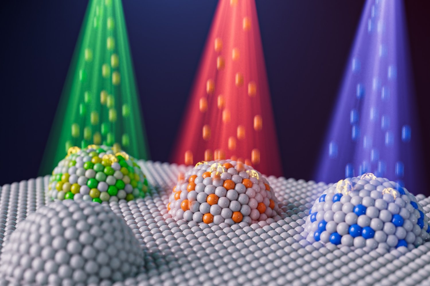
They typically do this by cooling the atoms to a stand-still, then using laser light to position the particles as close as 500 nanometers apart — a limit that is set by the wavelength of light. Now, MIT physicists have developed a technique that allows them to arrange atoms in much closer proximity, down to a mere 50 nanometers. For context, a red blood cell is about 1,000 nanometers wide.
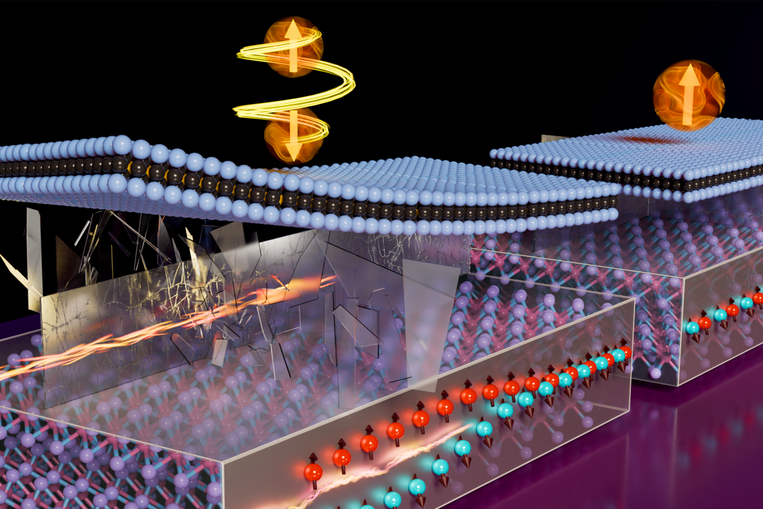
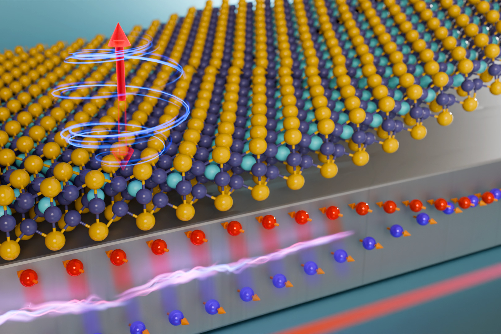
The physicists demonstrated the new approach in experiments with dysprosium, which is the most magnetic atom in nature. They used the new approach to manipulate two layers of dysprosium atoms, and positioned the layers precisely 50 nanometers apart. At this extreme proximity, the magnetic interactions were 1,000 times stronger than if the layers were separated by 500 nanometers.
What’s more, the scientists were able to measure two new effects caused by the atoms’ proximity. Their enhanced magnetic forces caused “thermalization,” or the transfer of heat from one layer to another, as well as synchronized oscillations between layers. These effects petered out as the layers were spaced farther apart.
“We have gone from positioning atoms from 500 nanometers to 50 nanometers apart, and there is a lot you can do with this,” says Wolfgang Ketterle, the John D. MacArthur Professor of Physics at MIT. “At 50 nanometers, the behavior of atoms is so much different that we’re really entering a new regime here.”
Ketterle and his colleagues say the new approach can be applied to many other atoms to study quantum phenomena. For their part, the group plans to use the technique to manipulate atoms into configurations that could generate the first purely magnetic quantum gate — a key building block for a new type of quantum computer.
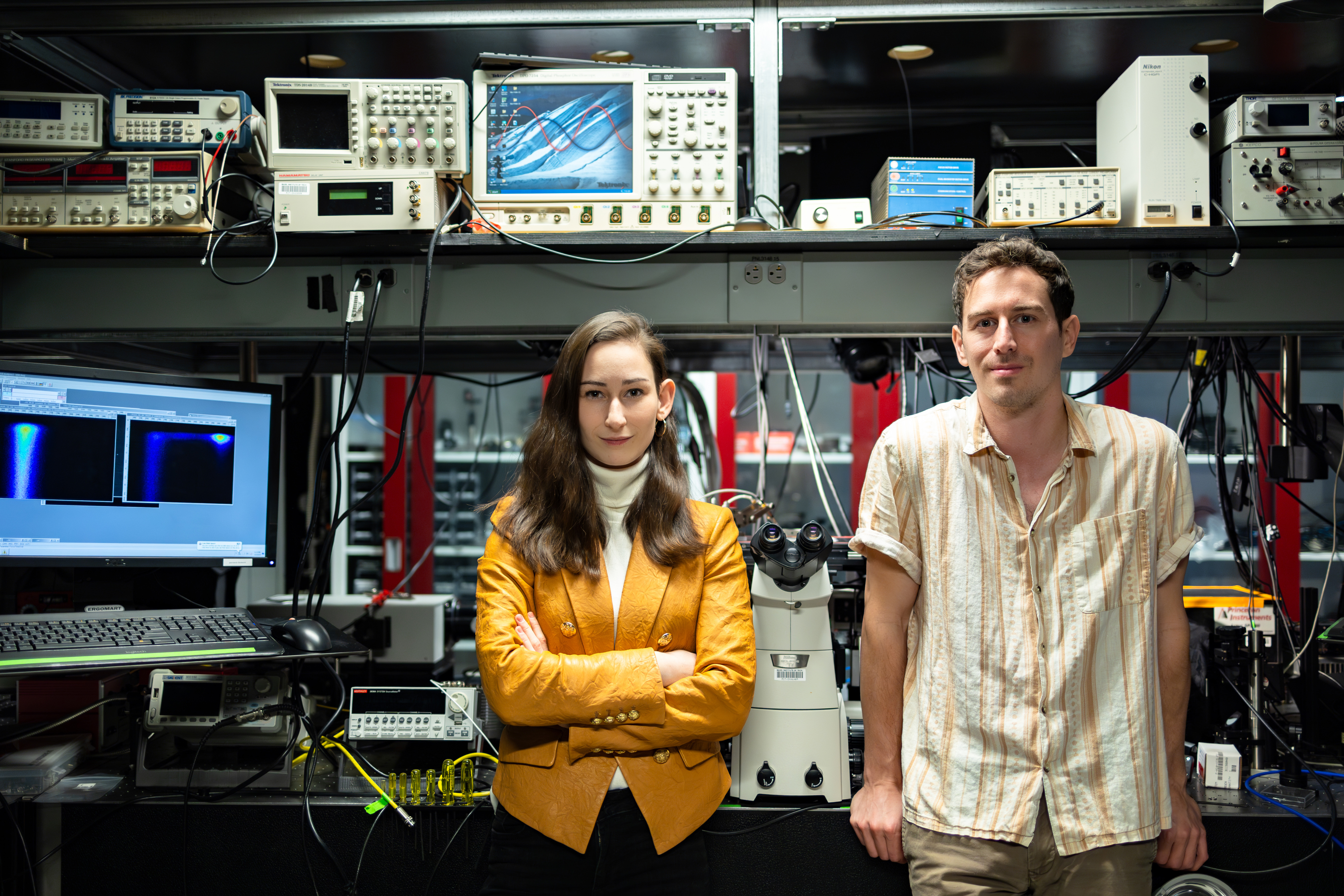
The team has published their results today in the journal Science. The study’s co-authors include lead author and physics graduate student Li Du, along with Pierre Barral, Michael Cantara, Julius de Hond, and Yu-Kun Lu — all members of the MIT-Harvard Center for Ultracold Atoms, the Department of Physics, and the Research Laboratory of Electronics at MIT.
Peaks and valleys
To manipulate and arrange atoms, physicists typically first cool a cloud of atoms to temperatures approaching absolute zero, then use a system of laser beams to corral the atoms into an optical trap.
Laser light is an electromagnetic wave with a specific wavelength (the distance between maxima of the electric field) and frequency. The wavelength limits the smallest pattern into which light can be shaped to typically 500 nanometers, the so-called optical resolution limit. Since atoms are attracted by laser light of certain frequencies, atoms will be positioned at the points of peak laser intensity. For this reason, existing techniques have been limited in how close they can position atomic particles, and could not be used to explore phenomena that happen at much shorter distances.
“Conventional techniques stop at 500 nanometers, limited not by the atoms but by the wavelength of light,” Ketterle explains. “We have found now a new trick with light where we can break through that limit.”
The team’s new approach, like current techniques, starts by cooling a cloud of atoms — in this case, to about 1 microkelvin, just a hair above absolute zero — at which point, the atoms come to a near-standstill. Physicists can then use lasers to move the frozen particles into desired configurations.
Then, Du and his collaborators worked with two laser beams, each with a different frequency, or color, and circular polarization, or direction of the laser’s electric field. When the two beams travel through a super-cooled cloud of atoms, the atoms can orient their spin in opposite directions, following either of the two lasers’ polarization. The result is that the beams produce two groups of the same atoms, only with opposite spins.
Each laser beam formed a standing wave, a periodic pattern of electric field intensity with a spatial period of 500 nanometers. Due to their different polarizations, each standing wave attracted and corralled one of two groups of atoms, depending on their spin. The lasers could be overlaid and tuned such that the distance between their respective peaks is as small as 50 nanometers, meaning that the atoms gravitating to each respective laser’s peaks would be separated by the same 50 nanometers.
But in order for this to happen, the lasers would have to be extremely stable and immune to all external noise, such as from shaking or even breathing on the experiment. The team realized they could stabilize both lasers by directing them through an optical fiber, which served to lock the light beams in place in relation to each other.
“The idea of sending both beams through the optical fiber meant the whole machine could shake violently, but the two laser beams stayed absolutely stable with respect to each others,” Du says.
Magnetic forces at close range
As a first test of their new technique, the team used atoms of dysprosium — a rare-earth metal that is one of the strongest magnetic elements in the periodic table, particularly at ultracold temperatures. However, at the scale of atoms, the element’s magnetic interactions are relatively weak at distances of even 500 nanometers. As with common refrigerator magnets, the magnetic attraction between atoms increases with proximity, and the scientists suspected that if their new technique could space dysprosium atoms as close as 50 nanometers apart, they might observe the emergence of otherwise weak interactions between the magnetic atoms.
“We could suddenly have magnetic interactions, which used to be almost neglible but now are really strong,” Ketterle says.
The team applied their technique to dysprosium, first super-cooling the atoms, then passing two lasers through to split the atoms into two spin groups, or layers. They then directed the lasers through an optical fiber to stabilize them, and found that indeed, the two layers of dysprosium atoms gravitated to their respective laser peaks, which in effect separated the layers of atoms by 50 nanometers — the closest distance that any ultracold atom experiment has been able to achieve.
At this extremely close proximity, the atoms’ natural magnetic interactions were significantly enhanced, and were 1,000 times stronger than if they were positioned 500 nanometers apart. The team observed that these interactions resulted in two novel quantum phenomena: collective oscillation, in which one layer’s vibrations caused the other layer to vibrate in sync; and thermalization, in which one layer transferred heat to the other, purely through magnetic fluctuations in the atoms.
“Until now, heat between atoms could only by exchanged when they were in the same physical space and could collide,” Du notes. “Now we have seen atomic layers, separated by vacuum, and they exchange heat via fluctuating magnetic fields.”
The team’s results introduce a new technique that can be used to position many types of atom in close proximity. They also show that atoms, placed close enough together, can exhibit interesting quantum phenomena, that could be harnessed to build new quantum materials, and potentially, magnetically-driven atomic systems for quantum computers.
“We are really bringing super-resolution methods to the field, and it will become a general tool for doing quantum simulations,” Ketterle says. “There are many variants possible, which we are working on.”
This research was funded, in part, by the National Science Foundation and the Department of Defense.
![]()
© Image: Courtesy of the researchers; MIT News